Introduction
COMMON-BASE amplifiers were described in Chapter 3 and common-emitter amplifiers in Chapter 4. This chapter is devoted to the third basic form of transistor amplifier circuit, the common-collector circuit. As in the earlier chapters we shall analyze the performance of the amplifier by deriving expressions for the input resistance, output resistance and voltage gain.
The fundamental circuit of a common-collector amplifier is given in Fig. 5.1 (a) in which R8 represents the resistance of the signal source and R1 represents the load resistance. For simplicity,
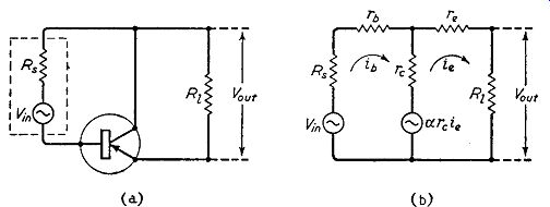
Fig. 5.1. The basic circuit/or the common-collector transistor amplifier
is given at (a), and the equivalent circuit at ( b) bias sources are omitted
from this diagram. In Fig. 5.1 (b) the transistor is represented by an equivalent
network of resistances re, Tb and re together with a voltage generator of
e.m.f. alpha_ierc where it is the alternating current in the emitter circuit.
If the base current ib and emitter current ie are both shown acting in clockwise
directions as in Fig. 5.1(b), then the current in the common collector
resistance re is the difference (ie - ib)-
From Chapter 2 we know that this difference is the collector current ic: all conventions are therefore satisfied in this diagram.
Input Resistance
Applying Kirchhoff's laws to the circuit of Fig. 5.1 (b) we have:
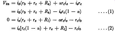
.... (1)
.... (2)
To find an expression for the input resistance we must eliminate ie between expressions (1) and (2) to obtain a relationship between Vin and ib, From (2)
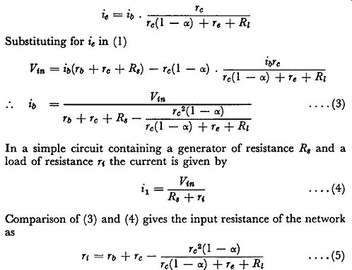
.... (3)
In a simple circuit containing a generator of resistance R8 and a load of resistance T' the current is given by
.... (4)
Comparison of (3) and ( 4) gives the input resistance of the network as:
.... (5)
which shows that the input resistance of the common-collector amplifier depends on the parameters of the transistor (rb, rc, Te and ex) and on the load resistance Rz.
This expression can be simplified slightly by combining the second and third terms. We then have
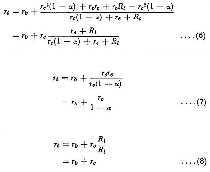
.... (6)
If R1 and re are small compared with rc(l - o:) the input resistance is given by:
.... (7)
If Rz is large compared with rc(1 - alpha) the input resistance is given by
.... (8)
Input Resistance for Junction Transistor as Common-collector Amplifier
For a junction transistor having r1, = 300 ohms, re = 25 ohms, re = 1 megohm, and alpha = 0.98, the input resistance for short circuited output terminals is given by expression (7), namely
The input resistance for open-circuited output terminals is given by expression (8)
r, = r1, + re
= 300 + 1,000,000 ohms
= 1 megohm approximately
The input resistance therefore increases considerably as the load resistance is increased, the curve having the shape shown in Fig. 5.2. For large values of load resistance the input resistance approaches the value of re, which can be as high as 2 megohms for junction transistors. This is by far the highest value of input
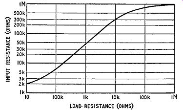
Fig. 5.2. Variation of input resistance with load resistance for a common-collector
amplifier resistance so far encountered for a circuit employing a junction
transistor; it is, in fact, comparable with the input resistance of a thermionic
valve amplifier which commonly has grid resistors of this value.
This high input resistance is the most useful property of the common-collector amplifier and the chief reason for its use.
Output Resistance
We can obtain an expression for the output resistance of a common-collector transistor amplifier by eliminating ib between (1) and (2), so as to obtain a relationship between ie and Vin, From (2)
we have…
Substituting for:
Multiplying numerator and denominator by
.... (9)
In a simple circuit containing a signal source of voltage V and internal resistance r0 feeding a load resistance Ri, the current i1 is given by
.... (10)
Comparing (9) with (10) we obtain the following expression for the output resistance To of the common-emitter amplifier:
.... ( 11)
Combining the second and third terms:
.... (12)
This expression shows that the output resistance depends on re, Tb, r c, alpha and the source resistance R8. When the source resistance is very small we have Tb ro = re + rc(1 - alpha) . -- Tb+ re For junction transistors rb is small compared with Tc and this expression simplifies to

(13)
When the source resistance R1 is very large compared with Tb and re, expression (12) simplifies to To= Te+ Tc(l - ex) .... (14)
Output Resistance far a Junction Transistor as Common-collector Amplifier
For a junction transistor having Tb = 300 ohms, re = 25 ohms, re = 1 megohm, and ex= 0.98, the output resistance for short-
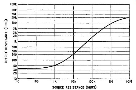
Fig. 5.3. Variation of output resistance with source resistance for a common-collector
amplifier
... circuited input terminals is, from expression ( 13), given by the following r0 = r, + (I - alpha_)rb = 25 + (1 - 0·98) 300 ohms = 25 + 300 x 0·02 ohms
= 25 + 6 ohms
= 31 ohms
For open-circuited input terminals, the output resistance is given by expression ( 14)
To= Te+ (1 - alpha_)Tc
= 25 + (1 - 0·98) x 1,000,000 ohms
= 25 + 1,000,000 X 0.02 ohms
= 20 k-O approximately
The variation of output resistance with generator resistance 1s illustrated in Fig. 5.3. For small values of generator resistance, the output resistance is very low, being only slightly greater than the emitter resistance Te.
It is easily possible, for example, to have an output resistance of less than 50 ohms: a value as low as this is impossible from common-base or common-emitter transistor amplifiers.
Thus a common-collector amplifier with a low value of generator resistance and a high value of collector load resistance can have a high value of input resistance and a low value of output resistance, conditions opposite to those normally encountered in transistor amplifiers and similar in fact to those which apply to a cathode follower using a thermionic valve.
Voltage Gain
From Fig. 5.1 (b) we can see that the output voltage is given by ie R1-
The voltage gain Vout/Vin is thus given by ieRz/Vin
From (9) ie is given by:
Hence:
.... (15)
This can be simplified by ignoring Te in comparison with the other terms in the first bracket of the denominator and by ignoring Tb in the second bracket. After further evaluation this gives:
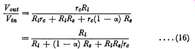
.... (16)
For a junction transistor exis always less than unity, and hence the denominator always exceeds Rz, giving a voltage gain of less than unity. If R, is small, the gain is very nearly equal to unity, another respect in which the common-collector amplifier is similar to a thermionic-valve cathode-follower circuit.
Consider a junction transistor having a source resistance (R,) of 1 k-ohm and a load resistance (Rz) of 100 kn. If alpha = 0.96 and re = 1 megohm we have, from expression (16) ...
Current Gain of Common-collector Amplifier
Expression (15) may be written Vout _ Rz + Te + Tc(1 - alpha)
Vin - R + + rc 2 (1 - alpha)
8 Tb Tc - ------- Rz + Te + Tc(1 - alpha)
and this can be expressed in the form TcRz Vout _ R1 + re + rc(1 - alpha)
Vin - R, + r,
where Tf is the input resistance (see expression 5).
This may be written Vout _ Rz Tc Vin - Ra + Tf Rz + Te + Tc(1- alpha)
If Rz and Te are small compared with Tc(1 - alpha) and Ra is small compared with Tt, the voltage gain becomes
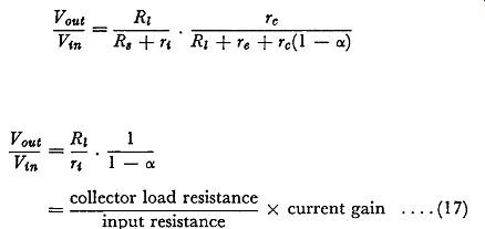
.... (17)
This expression is of the type used in Chapter 2 in the simplified calculations of stage gains of transistors and it suggests that the current gain of the common-collector circuit is equal to 1 / ( 1 - ex). This can be confirmed from equation (2).
which on simplification and for small collector load values gives the result:
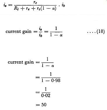
.... (18)
When exis nearly unity, as in junction transistors, the value of current gain can be very high. For example if ex= 0·98, we have:
The value of current gain for a common-collector amplifier is not very different from that for a common-emitter amplifier: when ex
is nearly unity, ex/(1 - ex) is not very different from 1/(1 - ex). In spite of this very high value of current gain, however, the common-collector amplifier gives less than unity voltage gain because the input resistance is so high compared with the load resistance. In fact if we equate expression ( 18) to unity we have the following approximate relationship
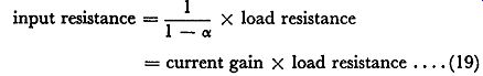
= current gain X load resistance .... ( 19)
Practical Circuit for a Common-collector Amplifier
A circuit diagram for a common-collector amplifier is given in Fig. 5.4 and the component values required in it can be calculated by methods similar to those employed for other amplifiers. For example, if the supply is 6 volts and the mean current in the load resistance is to be 1 mA, a convenient value for the load resistance is 3 k-O, this permitting a peak swing of emitter potential of 3 volts.
The quiescent emitter potential is thus -3 volts and the quiescent
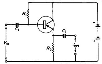
Fig. 5.4. Practical circuit of a common-collector amplifier base potential
will not differ very greatly from this value. The potential difference across
the base bias resistor R1 is thus approximately 3 volts and if the base current
is 20 µA ( corresponding to a value of alpha ' of 50) the bias resistance
is given by 3/(20 X 10^-8), i.e., 150 k-O. The capacitance C2 depends on
the resistance to which the output terminals of the common-collector amplifier
is connected.
The capacitance C1 depends on R1 and the input resistance of the amplifier which, as shown above, also depends on the load resistance.
If the load resistance is high, the net input resistance can be as much as 100 k-O and, for an a.f. amplifier, C1 can be 0.1 µF which has a reactance of approximately 31 k-O at 50 hz and gives a loss of less than 1 dB at this frequency.
An interesting feature of the common-collector amplifier is that signals applied to the output terminals give a signal output at the input terminals. In this respect, such amplifiers, when used as buffer stages, are not as perfect as thermionic-valve cathode followers. This property of the common-collector amplifier can be anticipated from Fig. 5.1 (b): the equivalent generator alpha_r cie is in the common shunt arm of the network and the two resistances Te and Tb are of approximately the same magnitude. Thus the network is very nearly symmetrical and a signal applied across Rz can produce an output across R8.