Introduction
WE have so far discussed the properties of simple amplifiers containing only a single transistor. Sometimes the power output and the gain of a single transistor are adequate but where greater gain is required, it is necessary to use a number of transistors connected in cascade to form a multi-stage amplifier.
Some multi-stage amplifiers are required to deliver an output voltage or output current which is small compared with the maximum that the final stage could deliver: usually this output is used as the input voltage or current for a following amplifier.
In the design of amplifiers of this type the aim is to minimize distortion in the output voltage or current and the power output of the final stage is of little consequence. Such amplifiers are termed small-signal amplifiers, voltage amplifiers or current amplifiers: typical examples are microphone head amplifiers and the r.f. and early i.f. amplifiers in a receiver.
The final stage of a multi-stage amplifier may, however, be required to drive a loudspeaker or a recording head or some other load requiring appreciable power for its operation. Such stages must deliver undistorted power and their design principles differ from those of small-signal amplifiers. Amplifiers with a final stage of this type are termed large-signal or power amplifiers.
The early stages of a large-signal amplifier can, of course, be regarded as constituting a small-signal amplifier.
In this chapter we shall consider the basic principles of small signal a.f. amplifiers using junction transistors. We shall assume common-emitter operation throughout and all the circuits require protective measures to stabilize d.c. operating conditions.
Current and Voltage Amplifiers
It is usual in the design of valve amplifiers to regard each class-A stage as a voltage amplifier, i.e., as a stage whose input signal is the output voltage of the previous stage and whose output signal applied to the following stage is a voltage which is a substantially faithful copy of the input voltage. If a stage is to be regarded as a voltage amplifier, it is essential that the voltage of the signal source should not be affected by the connection of the amplifier across it: this requires that the input resistance of the amplifier should be very high compared with the resistance of the signal source. The output voltage of the amplifier should be substantially unaffected by variations in the value of the load resistance: this requires that the output resistance should be low compared with the load resistance.
Thus a voltage amplifier must have a high input resistance and a low output resistance as shown in Fig. 7.1 (a). A class-A amplifying valve satisfies this requirement because the input resistance is nearly
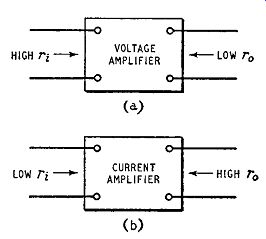
Fig. 7.1. Fundamental properties of (a) a voltage amplifier and ( b) a current
amplifier
…infinite, whereas the output resistance can be less than 1 k-O. Provided these resistance requirements are satisfied the gains of the individual stages of a voltage amplifier can be multiplied together to give the overall gain of the amplifier or (and this is another way of expressing the same fact) the gains of individual stages, when expressed in decibels, can simply be added to give the overall gain of the amplifier.
Similarly it is possible to have a current amplifier. When such an amplifier is connected to a signal source it is essential that the current flowing in the signal source should not be affected by the connection of the amplifier: this requires that the input resistance of the amplifier should be small compared with the resistance of the signal source. The output current from a current amplifier should ideally be independent of the load resistance: this requires that the output resistance should be high compared with the load resistance.
Thus a current amplifier must have a low input resistance and a high output resistance as shown in Fig. 7.1 (b). Provided these resistance requirements are satisfied, the gains of the individual stages of a current amplifier can be multiplied together to give the overall gain of the amplifier or ( and this is another way of expressing the same fact) the gains of the individual stages, when expressed in decibels, can simply be added to give the overall current gain of the amplifier.
As we have seen in previous chapters, a common-base or a common-emitter transistor amplifier stage has a small input resistance and a high output resistance. Both types of amplifier are therefore best regarded as current amplifiers. The common-collector amplifier, on the other hand, has a high input resistance and a low output resistance: this is best regarded, therefore, as a voltage amplifier.
The majority of transistor amplifiers are of the common-emitter type and the current gain of a particular stage is usually computed from the input (base-emitter) circuit to the input (base emitter) circuit of the following stage. If, as commonly occurs, both stages include similar types of transistor operating under similar d.c. conditions, these input circuits are likely to have equal input resistances. If this is so then the current gain from one input circuit to the next is numerically equal to the voltage gain from one input circuit to the next. Provided, therefore, the input circuits are of equal resistance, it is possible to calculate the gain in terms of voltage or current as desired. This point is illustrated in some of the calculations given later in this chapter.
RC-coupled a.f. Amplifiers
Two successive stages of a small-signal a.f. amplifier are illustrated in Fig. 7.2. RC-coupling is used and both stages are stabilized by the potential-divider method. Earlier chapters give the method of calculating the values of the emitter resistor, collector resistor and the potential-divider resistors.
The input resistance of a common-emitter transistor stage is commonly approximately 1 kn, but this is reduced by the arms of the potential divider which are effectively in parallel with it and we can take the net input resistance as 800 ohms. This is in parallel with the collector load resistance of the previous stage and if this is taken as 3·3 k-ohm the effective load resistance is thus 3 300 X 800 .
' = 640 ohms approximately 3,300 + 800
The gain of an amplifier with such a value of collector load resistance can be calculated in the following manner. Assume a collector signal current of ic in the transistor: the signal voltage across the load resistance is thus i0R0 . If the current gain is alpha_' the base current is i0 /alpha_'. The input resistance of the transistor
Fig. 7.2. A small-signal a.f amplifier consisting of two RC-coupled common-emitter stages is Ti and the input voltage which must be applied across Ti to produce a base current of ic/alpha_' is icrtfalpha_'. The voltage gain is thus given by
Vout alpha_'icRc Vin = icrt alpha_'Rc T;
Substituting
ex'= 50, Re = 640 ohms and ri = 1 kO
Vout = 50 X 640
Vin 1,000 = 32
This calculation shows that the input resistance of the second stage is low compared with the load resistor of the first stage and it virtually determines the voltage gain of the first stage. The value of the collector load resistance for the first stage does not greatly affect its voltage gain.
If both stages of the amplifier of Fig. 7.2 have a voltage gain of 32 the overall voltage gain is 322, i.e., approximately 1,000. The gain could alternatively be calculated from the mutual conductance of the transistor, i.e. the ratio of the signal-current output to the input voltage applied between base and emitter.
The mutual conductance of a transistor is directly proportional to the emitter current and inversely proportional to the absolute temperature. At 25°C it is given approximately by the expression gm= ~e where Ve= 25 mV Thus for an emitter current of 1 mA the mutual conductance is 40 mA/V and for a load resistance of 640 ohms the voltage gain is 25·6, less than the value deduced on the previous page.
The gain of the amplifier can be written A =gmRc leRc
Ve But, as shown on page 97, the gain is also equal to alpha_' Rc/rtn. Equating these two expressions for the gain we have giving:
This is a useful expression because it shows that if alpha_' = 50 the emitter current must be l ·25 mA to give an input resistance of 1 kO. For 1.25 mA emitter current gm is 50 mA/V and the gain for a load resistance of 640 ohms is 32, which agrees with the result deduced on the previous page.
Value of Coupling Capacitor
The capacitance C3 is determined by the low-frequency limit of the pass-band, the response being 3 dB down at the frequency for which the capacitive reactance equals the resistance effectively in parallel with C3
In this amplifier the resistance is, say, 800 ohms from the input of the following transistor and 3.3 k-O from the output circuit of the preceding transistor. If the low-frequency limit is 50 hz we have:
1 2efC3
= r 1 Ca=- 2 pi fr
--------F 6·284 X 50 X 4,100
= 0·8 µ.F approximately
Small-signal Transformer-coupled a-f. Amplifier
A circuit giving greater gain is that shown in Fig. 7.3 in which a transformer is used to couple the collector circuit of the first transistor to the base circuit of the second. For maximum gain the turns ratio of the transformer should be chosen to match the output resistance of the first transistor (commonly approximately 30 k-O) to the input resistance of the second (1 k-O).
The turns ratio required is thus radic (30,000/1,000) : I, i.e. 5·5 : 1.
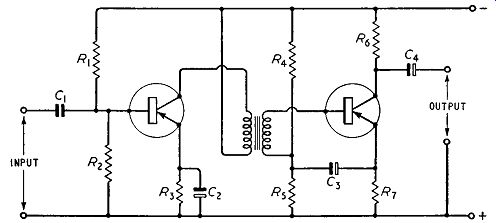
Fig. 7.3. A small-signal a.f. amplifier consisting of two transformer-coupled
common-emitter stages
As explained on page 145 perfect matching gives distortion because variations in input resistance affect the input current.
Lower distortion (and lower gain) can be obtained by using a smaller turns ratio, thus tending to drive constant current into the following transistor.
The primary is, of course, the larger of the two windings and this is connected to the collector circuit so as to step down the voltage applied to the following base. There is, of course, an equal step up in current and as transistors are current-operated devices the transformer gives gain greater than is obtainable from the RC coupled amplifier.
We can confirm this by calculation in the following manner.
When the turns ratio is correct, the collector load presented to the first transistor by the transformer primary winding is 30 k-O. This is equal to the output resistance of the first transistor, and the gain is thus half that which would be obtained if the output resistance were very large*. Thus the voltage gain from base to collector of the first transistor is equal to that of a high-impedance source
* A similar calculation for an r.f. amplifier is given on page 110.
feeding a load resistance of 30 k-ohm./2, i.e. 15 k-O., and is given by gmRl = 50 X 10^-3 X 15 X 10^3 = 750
in which the mutual conductance of the transistor is taken as 50 mA/V. This gain is reduced in the ratio 5·5 : l by the trans former and hence the voltage gain from the base of the first transistor to the base of the second is given by
750 = 135 approximately 5.5
This is more than 4 times the gain from the RC-coupled amplifier.
Calculation of Transformer Primary Inductance
The primary inductance of the transformer is determined by the lowest frequency it is desired to amplify. There is a loss of 3 dB at the frequency for which the inductive reactance is equal to the effective resistance of the collector circuit: this resistance is composed of the output resistance of the transistor and the load resistance at the transformer primary. Normally these two resistances are each equal to 30 k-O. and the effective resistance is 15 kO. If a loss of 3 dB at 50 hz is acceptable, the primary inductance required can be calculated thus:
2 pi fL = 15,000 L = 15,000 2 pi f
_ 15,000 H 6.284 X 50
= 50 H approximately
NEGATIVE FEEDBACK IN SMALL-SIGNAL AMPLIFIERS
Negative feedback is employed in transistor amplifiers for a number of reasons: it reduces distortion and makes the performance of the amplifier less dependent on transistor parameters and hence less dependent on temperature. In addition feedback can be used to extend the frequency response and to give the amplifier desired values of input or output resistance.
There are two basic feedback circuits and they are illustrated in Fig. 7.4. In circuit (a) feedback is applied by connecting a resistor Rb between the collector and the base. This circuit is also used to improve the d.c. stability of the common-emitter amplifier.
In the second basic circuit illustrated at (b) feedback is applied by inclusion of an un-decoupled emitter resistance Re, Circuit (a) has the effect of reducing the input resistance of the amplifier and may be used as the input stage of a current amplifier where the input resistance must be small compared with the resistance of the signal source. This form of feedback decreases
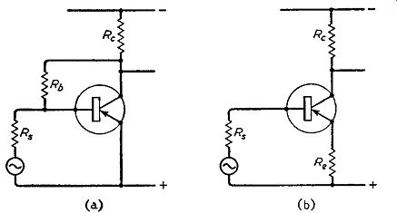
Fig. 7.4. (a.) (b)
Essential connections for two methods ef applying negative feedback to common-emitter transistor amplifiers the output resistance of the amplifier and is useful where the output is required in the form of a voltage and the output resistance must be small compared with that of the following load. This circuit is therefore likely to be used with a current input and a voltage output, and the gain measured in these terms can be evaluated in the following way.
If the current flowing into the base is ib, the current in the collector circuit is clib and this, in flowing through the collector load resistance Re, gives rise to a collector voltage of r:x'ibRc, This, in turn, gives rise to a current of:
r:x'ibRc/Rb in the resistor Rb,
The total input current i,n required is thus given by
If Rb is removed, the input current is, of course, simply ib and the effect of feedback is thus to reduce the input resistance to 1/(1 + a'Re/Rb) of its former value. If Rb is small compared with a' Re the input resistance is Rb /a' Re of its former value. The gain* of the circuit is given by output voltage a'ibRe input current
If Rb is small compared with a' Re this reduces to output voltage = Rb input current which is independent of the transistor parameters and of Re.
Circuit (b) has the effect of increasing the input resistance of the amplifier and is used as the input stage of a voltage amplifier.
This form of feedback increases the output resistance of the amplifier and is useful when the output is required in the form of a current and the output resistance must be large compared with the value of the following load resistance. Such a circuit is likely to be used with a voltage input and a current output, and its gain, measured in these terms, can be evaluated in the following manner.
If the signal current flowing into the base is ib, the current in the collector circuit is a'ib. The current in the emitter circuit is ( a' + 1) ib and this, in flowing through the emitter resistor Re, gives rise to an emitter voltage of (a' + 1 )ibRe. Provided Re is large enough this voltage is large compared with the base-emitter voltage and the input signal voltage required is approximately (a' + l)ibRe, giving the input resistance as (a' + l)Re. The gaint is given by output current a'ib input voltage (a' + l)ibRe As a' is normally large compared with unity, (a' + 1) is approximately equal to a' and we have output current _ 1 input voltage - Re which is independent of the transistor parameters and of the load resistance Re.
Two-stage Current Amplifier
A transistor stage of the type illustrated in Fig. 7.4 (a) gives a voltage output for a current input, whereas a stage of the type shown ...
* Strictly mutual resistance. t Strictly mutual conductance.
... in Fig. 7.4 (b) gives a current output for a voltage input. By combining a stage of each type it is possible to produce a two-stage current amplifier or a two-stage voltage amplifier. For example by combining a first stage of type (a) with a second stage of type (b)
we obtain an amplifier with a low input resistance and a high output resistance, i.e. a current amplifier.
In such a combination of the circuits of Figs. 7.4 (a) and (b) the feed back resistor Rb bridges the base and collector of the first transistor. It is, however, more usual in two-stage current amplifiers for Rb to be connected between the base of the first transistor and the emitter of the second as shown in Fig. 7.5 which also includes ...
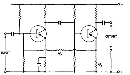
Fig. 7.5. A two-stage transistor current amplifier with low input resistance
and high output resistance
...components for d.c. stabilization. The two circuits are strictly equivalent because the signal voltage at the collector of the first transistor is equal to that at the base of the second transistor which is, in turn, equal to that at the emitter of the second transistor. Thus the same feedback is obtained whether Rb is returned to the collector (as in Fig. 7.4 (a) ) or to the emitter (as in Fig. 7.5). It is, in fact, preferable to use the circuit of Fig. 7.5 because the feedback then reduces any distortion arising in the inter-transistor coupling network.
A signal current iin applied to the input of the amplifier of Fig. 7.5 gives a signal voltage of itnRb at the collector of the first stage.
The output resistance of this stage is low and the input resistance of the second stage is high. Hence this voltage is not reduced by the addition of the second stage and becomes the input for this stage. The (output current)/(input voltage) ratio for the second stage is equal to l /Re and the signal current output of the amplifier is thus itnRb/Re. The overall current gain is thus given by R_B/Re and is independent of the transistor parameters.
Two-stage Voltage Amplifier
By combining a first stage of the type shown in Fig. 7.4 (b) with a second of type Fig. 7.4 (a) we obtain an amplifier with a high input resistance and a low output resistance, i.e., a voltage amplifier.
The circuit is given in Fig. 7.6 with components for d.c. stabilization. As shown in Fig. 7.6 it is usual in two-stage amplifiers for …
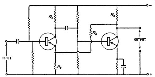
Fig. 7.6. A two-stage transistor voltage amplifier having high input resistance
and low output resistance
… the feedback resistor Rb to be returned to the emitter of the first stage rather than to the base of the second. This modification does not affect the action of the feedback because Rb provides a feedback current which must be connected in parallel with a signal current of the correct phase. Now the signal current in the base circuit of the second transistor is the collector current of the first transistor and also flows in Re. Thus it does not matter whether Rb is returned to the base of the second stage or the emitter of the first.
The second alternative is generally preferred because the feedback is then able to reduce any distortion occurring in the inter-transistor coupling network.
A signal voltage V_in applied to the input of the amplifier illustrated in Fig. 7.6 gives a current output of Vin/Re from the first stage. The output resistance of this stage is high and the input resistance of the second stage is low: hence this current is not reduced by the connection of the second stage and is the input for the second stage. The (output voltage)/(input current) ratio for the second stage is equal to Rb and the output voltage is V_in Rb/Re, The overall voltage gain is hence Rb/Re, This is the same expression as for the current gain of the amplifier previously described and is independent of the transistor parameters and of the value of the collector load resistors.
As a numerical example consider a voltage amplifier of the type illustrated in Fig. 7.6. We have shown before that a suitable value for Re is 3.3 k-ohm and we will take alpha ' as 50 for both transistors. alpha 'Rc is thus 165 k-ohm and Rb must be small compared with this for the second transistor to have adequate feedback. A suitable value for Rb is 20 k-oh. Re should have a value such that the signal voltage across Re is large compared with that across the base-emitter junction. If we take the resistance of this junction as r,, a voltage V_in across it gives rise to an input current of Vin/r, which, in turn, gives an emitter current of approximately alpha 'Vin/r, and a voltage across the emitter resistor of alpha 'Vin Re/r,. The ratio of the voltage across Re to the base-emitter voltage is thus alpha 'Re/r,, i.e., gm Re, and this should be large compared with unity. If gm is 50 mA/V, Re can be 100 ohms, giving gm Re as 5. The overall voltage gain of the amplifier is given by Rb/Re, i.e. 20,000/100, which is equal to 200.