Introduction
WE have so far confined the discussion of transistor amplifiers to those used at low frequencies, particularly audio frequencies.
In this frequency range transit-time effects and the effects of internal capacitances within the transistor are in general negligible. At higher frequencies, and in particular at radio frequencies, these effects are significant and cause the gain to fall below the values obtainable at lower frequencies.
The effects of transit time within the transistor were discussed in Chapter 2 where it was mentioned that this effect can be allowed for by assuming that the current amplification factor falls with frequency according to the expression:
a= alpha_0 / __/ (1 + f^2/f_alpha ^2)
in which f_alpha is the alpha cut-off frequency.
Of the various internal capacitances within a junction transistor, that between the collector and the base has the greatest effect on the high-frequency performance. In practice the effects of this capacitance are often more important than the fall in current amplification factor.
In a transistor r.f. amplifier the capacitance between collector and base provides feedback from the output to the input circuit.
This is illustrated in Fig. 8.1 (a) in which the capacitance Cbc is shown connected directly between collector and base terminals.
However, a better approximation to the performance of a transistor at high frequencies is obtained by assuming that the collector capacitance is returned to a tapping point b' on the base resistance as shown in Fig. 8.1 (b).
This modifies the feedback which now occurs via Cb'c and Tbb' in series and the high-frequency performance of the transistor is now dependent on the time constant Tbb' Cb'c which is probably the most important characteristic of a transistor intended for high frequency use.
The effect of this internal feedback connection is similar to that of the anode-grid capacitance of a triode valve; that is to say, if a resonant circuit is included in the base circuit (as is likely in an r.f. or i.f. amplifier) rbb' cb’e give positive feedback at frequencies ...
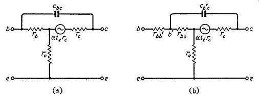
Fig. 8.1. T-section equivalent circuit of a transistor showing collector
capacitance, (a) returned to base input terminal and ( b) returned to a tapping
point on the base resistance.
...to one side of the resonance value and negative feedback at frequencies to the other side. In a triode valve the positive feed back is usually sufficient to cause oscillation but in a transistor amplifier this does not always occur because of the low input resistance. However, the change in the nature of the feedback around the resonance frequency makes the response curve of the amplifier asymmetrical and it is therefore desirable to include neutralizing components in order to minimize the effects of the internal feedback.
Transistor r.f. and i.f. amplifiers can be connected in common base or in common-emitter modes. Chapters 3 and 4 show that the common-emitter amplifier has higher power gain than the common-base type. This advantage of the common-emitter amplifier holds for all frequencies below the v.h.f. range. Maximum gain can only be achieved, of course, by perfect matching between the output circuit of one transistor and the input circuit of the succeeding one.
Such matching is difficult, particularly at radio frequencies, when there is a marked difference in value between the input and output resistances as for a common-base amplifier. The problem is not so acute for a common-emitter amplifier, for which the difference between the two resistances is not so great, and in practice this type of amplifier usually gives IO dB or more power gain than the common-base type.
Neutralizing is not difficult at frequencies that are well below the alpha cut-off value but becomes progressively more difficult as the cut-off frequency is approached. It is usually advisable, ...
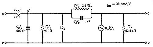
Fig. 8.2. A ff-section equivalent circuit of a uniform-base junction transistor
... therefore, that the operating frequency should not be above f al 10 or at worst f al 5: for example, the transistors used in 465 khz i.f. amplifiers generally have alpha cut-off frequencies of not less than 5 Mhz.
The T-section equivalent circuits of Fig. 8.1 are not well suited for calculating the performance of an r.f. or i.f. amplifier which uses resonant circuits as coupling elements and the equivalent 1r-section 1s preferred. This is illustrated in Fig. 8.2 in which gmVb'e ...
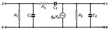
Fig. 8.3. At a single frequency the ff-section equivalent circuit <if
Fig. 8.2 can be reduced to this form.
... represents a constant-current generator. Also indicated on Fig. 8.2 are typical capacitances and resistances for a uniform-base junction transistor. This diagram may be used at any radio frequency but it is possible to simplify it to the form shown in Fig. 8.3 when operation is confined to a very small frequency range as in a transistor i.f. amplifier. This is a particularly useful equivalent circuit because it shows that the signal source is connected to a parallel RC combination R1 C1 and the output load is connected to the parallel RC combination Ra Ca, As the source and load impedances are both likely to contain resonant circuits the values of R1 and Ra are important because they damp these circuits, reducing the working Q. value and degrading selectivity. If C1 and C2 were constant they would be comparatively unimportant because any effect they had on the tuned circuit could be offset by an adjustment of the inductance or the capacitance of the tuned circuits.
Unfortunately C1 and Ca both depend on the d.c. operating conditions of the transistor and vary with changes in these conditions such as those produced by a.g.c. action. Their values and variations are thus important.
Uni-lateralization
R3 and C3 are the components which provide the internal feedback path between collector and base. As already pointed out, this feedback is undesirable because it causes asymmetry in the amplifier ...
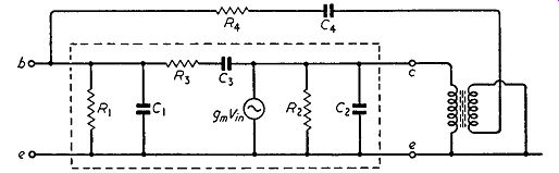
Fig. 8.4. Method of uni-lateralizing a junction transistor by means of a
phase-inverting transformer and components R, and C,
... response curve or possibly instability. It also causes interaction between the input and output tuned circuits and can make alignment of the amplifier difficult.
To avoid these effects, feedback due to Rs and Cs must be eliminated and the usual method is to apply an equal degree of feedback of opposite phase to the amplifier by means of an external RC network. From a point where the signal voltage is in antiphase to that at the collector a series RC network is returned to the base as shown in Fig. 8.4. If this signal voltage is equal to the collector voltage, the values of R, and C, required in the external feedback loop are equal to R3 and C3 (1,800 ohms and 10 pF are typical values for a uniform-base transistor). In a practical circuit, as shown later, the anti phase voltage is usually smaller, say 1 /nth of the collector voltage, and the external feedback components should then be R3/n and nC3 for equality of external and internal feedback.
When the effects of Ra and Ca are thus eliminated, the input and output circuits of the transistor are completely divorced and the equivalent circuit reduces to the simple form shown in Fig. 8.5.
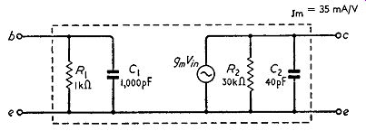
Fig. 8.5. For perfect uni-lateralization the equivalent circuit for a uniform-base
transistor reduces to this form
The transistor now is truly a " one-way " device in which the output circuit has no effect on the input circuit: for this reason the transistor is described as uni-lateralized. Unilateralization is essential when it is required to obtain without instability the maximum gain of which the transistor is capable.
It is possible to reduce (though not eliminate) the effects of Ra and Ca by omitting R4 and using a capacitor only in the external feedback circuit: this technique is known as neutralization.
Maximum Gain of r.f. Transistor
Typical values of R1 , R2, C1 , C2 and the constant-current generator for a uniform-base transistor operating at the intermediate frequency of 465 khz are indicated on Fig. 8.5. Not surprisingly, the input resistance is approximately 1 k-O and the output resistance 30 k-O: these are the values which apply to an a.f. amplifier. From these component values we can calculate the maximum gain in the following way. C1 and C2 are considered absorbed into the input and output tuned circuits and the gain is a maximum when the inter-stage coupling is designed to match the output resistance (R2) of one stage to the input resistance (R1) of the following stage.
If a transformer is used its turns ratio must be __/ (30,000)/(1,000) : I
= __/30 : I = 5·5 : 1 as before.
The constant-current generator then operates into a load of 15 k-ohm and the voltage gain is given by:
gmRl = 35 /1,000 X 15,000 = 525
The gain from the base of one transistor to the base of the following one is hence 525/5.5 = 95. This is the maximum gain which can be achieved and it is not reached in practice because, as explained later, the tuned circuits give an insertion loss.
If we repeat this calculation in general terms, taking the input resistance as rt and the output resistance as r0 , we have for perfect matching that the constant-current generator operates into a resistance or r0 /2 and the gain, from base to collector, is gmro/2. The matching transformer has, however, a step-down turns ratio of __/(r0 /rt) : I and the maximum gain (losses in the transformer being ignored) is given by:
The gain hence depends on the mutual conductance, the input resistance and the output resistance and can be improved by increase in any of these quantities. This expression gives the maximum gain from the base of the transistor to the base of the succeeding one. If the input resistances of both transistors are assumed equal, the maximum gain can be expressed in decibels thus:
For a uniform-base junction transistor having gm = 35 mA/V, rt = 1 k-O and r0= 30 k-O the maximum gain is given by:
= 40 dB nearly
To realize this gain it is essential that the transistor should be uni-lateralized. For without uni-lateralization there is interaction between the input and output circuits which has the effect of lowering both input and output resistances, thus lowering the gain as indicated in the above expression.
Design of Small-signal r.f. and i.f. Amplifiers
Because of the low input and output resistances of a common emitter amplifier the design of r.f. and i.f. transformers for transistors is a different problem from that of designing transformers for valve amplifiers.
In valve amplifiers the tuned circuit can be designed without regard to the input and output resistances because these are so high that they impose negligible damping on the circuits. The performance of the transformers is thus independent of the properties ...
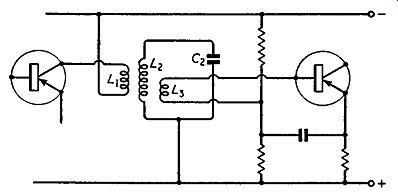
Fig. 8.6. Essential features ef a transistor r.f.
or i.j. amplifier: for simplicity neutralizing components are omitted.
...of the valves preceding and following them. In a transistor amplifier, however, the performance of the transformer is almost completely determined by the properties of the transistor.
The design of a transistor r .f. or i.f. amplifier is, in fact, determined by two considerations:
(a) to secure maximum gain the inter-stage tuned circuit must match the feeding to the terminating resistance;
(b) to obtain the desired selectivity, the coupling between the two transistors and the tuned circuit must be such that the circuit has the required value of working Q.
Fig. 8.6 illustrates one circuit which can be used. The tuned circuit L2C2 is coupled to the collector circuit of the first transistor by the primary winding L1 and to the base circuit of the second transistor by the tertiary winding L3. We shall assume that all the windings are unity-coupled. The turns ratio between L1 and L3 must match a generator of 30 k-O to a load of 1 k-O and must hence have a turns ratio of 5 ·S : 1 as in transistor a.f. amplifiers.
This satisfies requirement (a) above.
In mass production of receivers it may be desirable to depart from perfect matching to obtain satisfactory results in spite of spreads in transistor parameters and uni-lateralizing components.
Insertion Loss
The damping due to the two transistors can be calculated separately but it is easier to combine their effects by omitting, say, the tertiary winding and to assume that the primary is connected to a 15-k-O resistance, i.e. two 30-k-O in parallel (one due to transistor 1 and the other due to transistor 2). We now have to calculate the turns ratio of L1 to L2 for this determines to what extent the tuned circuit is damped. If a working Q. value of 100 is required, this could be obtained by using a circuit with an undamped Q. of, say, 120 which is reduced to the required value by the damping due to the transistors: in this example the damping is very light.
Alternatively, the tuned circuit could be designed to have a much higher undamped Q. value-say 300-which is again damped by the transistors to the required value of 100: the damping in this example is very heavy. Both these alternatives yield a tuned circuit with a working Q. value of 100 but the gain of the amplifier is not the same for both examples. We can show this in the following way.
Consider first the example of light damping. To reduce an undamped Q. from 120 to 100, the resistance effectively transferred by the primary circuit to the tuned circuit must be five times the dynamic resistance. This also means, of course, that at the resonance frequency the tuned circuit effectively connects across the primary winding a resistance equal to one-fifth that due to transistor damping. This reduces the effective load resistance to one-sixth of its value before the tuned circuit was connected, thus reducing the voltage_ gain to one-sixth. This represents an insertion loss of 15.6 dB and if, as assumed earlier, the maximum gain is 40dB the gain realised in practice is only 24.4 dB. Now consider the example of heavy damping. To reduce the Q. to one-third, the resistance effectively transferred by the primary circuit to the tuned circuit must be one-half the dynamic resistance.
This also means that at the resonance frequency the tuned circuit effectively connects across the primary winding a resistance equal to twice that due to transistor damping. This reduces the effective ...
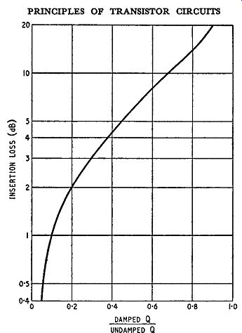
Fig. 8.7. Dependence of insertion loss on the ratio of damped to undamped
Q values.
... load resistance to two-thirds the value before the tuned circuit was connected, thus reducing the voltage gain in the same ratio.
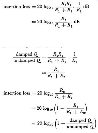
The insertion loss due to the tuned circuit is now only 3 ·5 dB and a practical gain of 36·5 is possible, if the theoretical maximum gain is 40 dB. To avoid a great insertion loss, therefore, the damping of the tuned circuit must be heavy. On the other hand, with a great reduction in Q there is a danger of large and unwanted variations in Q and hence in selectivity if for any reason (such as a change in a.g.c. voltage) the damping due to either transistor alters. In the compromise solution sometimes adopted, the reduction in Q due to transistor damping is 2:1, giving an insertion loss of 6 dB. For transistors with the parameters assumed above the voltage gain is then approximately 45, i.e., 34 dB. If the above calculation is repeated in general terms a curve can be prepared which expresses the insertion loss in terms of the ratio of working Q, value to undamped Q, value. This can be shown in the following way.
Basically an inter-transistor coupling which includes an LC circuit can be regarded at resonance as two resistances connected in parallel and fed from a constant-current source. One resistance, which we will call R1 , is that due to the collector circuit of the transistor feeding the tuned circuit and the base circuit of the transistor following the tuned circuit. The second resistance, which we will call R2, is the resistance effectively connected in parallel with R1 by the tuned circuit. R2 depends on the dynamic resistance of the tuned circuit and, if the tuned circuit is connected directly in the collector circuit, is equal to the dynamic resistance.
When the tuned circuit is connected, the load for the transistor becomes
R1R2/(R1 + R2 ).
It was formerly R1 and thus the insertion loss is given by insertion loss = 20 log10 R R1R2
. R1 dB 1 + R2 1
= 20 log10 R2 dB R1 + R2
The resistance R2 of the tuned circuit is effectively reduced to R1R2/(R1 + R2 ) when it is connected in circuit and thus the ratio of damped Q, to undamped Q, is given by We thus have damped Q, undamped Q, R1R2 R1 + R2 R2 R1
---- R1 +R2 insertion loss = 20 log10 R2 R1 + R2
= 20 log10 (1 - Ri ) R1 + R2
= 20 log10 (1 - damped Q, ) undamped Q, and this is the expression from which Fig. 8. 7 was plotted.
Primary Capacitance
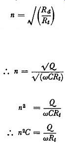
If the transistor damping is equivalent to a single resistance Rt across the primary winding, the turns ratio n : 1 required for a 2 :1 reduction in Q. is given by n = J(!:) being a step-up ratio if the dynamic resistance Rr1, exceeds Rt as is usual in practice. The dynamic resistance is given by Q.Lw or Q.JwC. Substituting Q./wC for Rr1, n = vQ. v(wCRt)
from which n2
- wCRt Q. n2C = Q. wRt
Now n2C is the effective capacitance across the primary winding and it is an important quantity because it must be large compared with the variations in transistor output capacitance which occur...
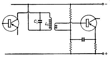
Fig. 8.8. Simple form of transistor r-f or i.f. amplifier: neutralizing
components are again omitted.
... when the a.g.c. voltage changes. As shown in the equivalent circuit (Fig. 8.5), the output capacitance of a uniform-base r.f. transistor is of the order of 40 pF but it can change by as much as 20 pF due to changes in bias. To minimize mistuning errors due to this variation, the primary capacitance must be large. For example, if the primary capacitance is 1,000 pF, a change of 20 pF in output capacitance represents a 2 percent variation in net capacitance and a 1 percent variation in resonance frequency. At 465 khz this is equivalent to nearly 5 khz.
The above expression shows that the primary capacitance depends on Q., w and Rt.
Now, for a particular amplifier and transistor all these quantities are fixed and hence the primary capacitance is also fixed. If Rt = 15 k-O, Q. = 200 and w = 2 pi X 465 khz we have
n^2 C = [200 / [6.284 X 465 X 10^3 X 15 X 10^8]] F
= 4,560 pF
For such a large value of effective primary capacitance the mis tuning due to a 20 pF variation in transistor output capacitance will be of the order of only 1 khz, which is acceptable.
The primary capacitance is independent of the value of n and we can therefore make n any value we please. If we make n unity, the primary winding has the same number of turns as the secondary winding and there is thus no need for both windings. The tuning capacitance of 4,560 pF can be placed across the primary winding and the secondary winding can be omitted. This now reduces the inter-transistor transformer to the simple form shown in Fig. 8.8 which still, however, gives the required selectivity characteristic and transistor matching.
A value of C1 (Fig. 8.8) as large as 4,560 cannot conveniently be made variable and in a circuit of this type, tuning is best achieved by adjusting the inductance L1 by movement of a dust-iron or ferrite core. !fit is considered essential to tune by means of a variable capacitor the circuit of Fig. 8.6 can be used, the value of n being so chosen that C2 has a small capacitance such as 200 pF: a variable capacitor can then be used for C2. Uni-lateralization So far we have omitted components for unilateralization in order to keep the circuits simple. To add these components we require a point on the transformer where the signal voltage is in antiphase to that at the collector. There is no need to add a winding specially for these components: the tertiary winding which feeds the base of the succeeding stage can be used, provided that the ends are chosen to give the required phase relationship. The circuit is shown in Fig. 8.9. The values of Rn and Cn are given by R3/n and nCa (see Fig. 8.4 for Ra and Ca) and the turns ratio between L1 and La is 5·5 : I for matching purposes. Thus for a transistor having internal feedback equivalent to 1.8 k-O and 10 pF we have Rn =Ra n
= 1,800 ohms 5·5
= 330 ohms
Cn = nCa
= 5.5 X 10 pF
=55 pF
Use of Drift Transistors as r.f. or i.f. Amplifiers
It is mentioned in Chapter 2 that drift transistors have a better performance at high frequencies than uniform-base transistors and can, in fact, be satisfactorily used at v.h.f. The adoption of the
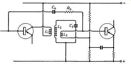
Fig. 8.9. Complete circuit of common-emitter transistor rj. or i.f amplifier
including uni-lateralizing components Rn and Cn graded-base impurity content
makes the output resistance of the drift transistor considerably higher than
for the uniform-base type.
For example at 465 khz a typical value for the output resistance of a drift transistor is 0.5 M-ohm compared with 30 k-O for the uniform base transistor. The input resistance and the mutual conductance of the drift transistor do not differ greatly from the values for a uniform-base transistor. The increased output resistance results in a significant improvement in gain as illustrated by the expression for the maximum gain:
. . gm2 r,ro maximum gam = 10 log10 - 4
Substituting the numerical values for a drift transistor
. . (35 X 10^-3) 2 X 10^3 X 0.5 X 10^6 maximum gam = 10 log10 4
= 52 dB nearly
This represents an improvement of nearly 12 dB over the maximum gain available from a uniform-base transistor although, of course, the maximum gain cannot be realised in practice because of the insertion loss of the tuned circuits which must be used.
The capacitances of a drift transistor are less than those of the uniform-base type. Typical values are: input capacitance = 100 pF output capacitance = 5 pF internal feedback capacitance = 1.5 pF
Use of Drift Transistors at 465 khz
The small value of the internal feedback capacitance in the drift transistor means that there is less danger of instability or of asymmetry of the frequency response curve than for a uniform-base transistor and, in fact, provided gain well below the theoretical maximum is accepted it is possible to dispense with uni-lateralization or neutralizing altogether both at 465 khz and at 10.7 Mhz.
However, if very high gain is essential uni-lateralization is advisable.
The circuit illustrated in Fig. 8.9 can then be used, the values of Rn and Cn being calculated as previously explained. For a drift transistor typical values for the internal feedback resistance and capacitance are 10 k-O and 1.5 pF. It is not usual to attempt to match the very high output resistance to the input resistance of the following stage and transformer ratios of 7:1 are common. For this ratio the values of the uni-lateralizing components are 1.4 k-O and 10.5 pF. Usually, however, a greater value of capacitance is used to allow for the effects of stray capacitance in the wiring to the transistor which inevitably increases the effective value of the feed back capacitance. The gain obtainable from such a stage of amplification at 465 khz is commonly 10 dB greater than is possible from a uniform-base transistor.
Use of Drift Transistors at 10.7 Mhz
The introduction of drift transistors has made possible the construction of transistorized v.h.f. receivers, e.g., f.m. receivers for use in Band II (87.5 to 100 Mhz in this country and 87.5 to 108 Mhz in U.S.A.). Such receivers are usually superheterodyne types and require an i.f. amplifier with a bandwidth of approximately 200 khz (for transmissions with a deviation of 75 khz) centered on the standard intermediate frequency of 10·7 Mhz.
Drift transistors can be used in such an i.f. amplifier but their characteristics at this frequency differ markedly from those which apply at the lower intermediate frequency of 465 khz. The following are typical values of the significant parameters at 10·7 Mhz: input resistance = 330 ohms input capacitance = 65 pF
output resistance = 1 7 k-O
output capacitance = 5 pF
internal feedback capacitance = 1.5 pF
mutual conductance = 30 mA/V
The input resistance, output resistance and mutual conductance are less than at 465 khz and limit the maximum gain at 10·7 Mhz as indicated in the following calculation:
. . gm2 r,ro maximum
gam = 10 log10 - 4
(30 X 10^-3) 2 X 330 X 17 X 10^3
= 10 log10 4
= 31 dB
The value of input resistance quoted above (330 ohms) applies when the output circuit of the transistor is short-circuited. If the transistor were unilateralized this would also be the input resistance of a practical amplifier. Commonly, however, drift transistors are not unilateralized or are deliberately mismatched and conditions in the output circuit affect the input circuit. For normal values of collector load the input resistance is less than for a short-circuited output circuit and a value of 150 ohms may be taken as typical at 10.7 Mhz.
Similarly the value of the output resistance quoted above ( 17 Hl)
applies when the input circuit of the transistor is short-circuited.
If unilateralization is not used the output resistance for normal values of source resistance may be taken as 6 k-O at 10.7 Mhz.
Substitution of these amended values of input and output resistance gives the maximum gain for non-unilateralized drift transistors at 10.7 Mhz as:
which is 8 dB less than the value for the unilateralized transistor.
This is not a very high gain and practical gains must inevitably be lower because of the insertion losses of the tuned circuits employed.
The insertion loss is therefore kept to a minimum by so designing the i.f. amplifier that the tuned circuits are very heavily damped by the input and output resistances of the transistor. It is possible in this way to reduce the insertion losses to 3 dB per stage thus giving a stage gain of 20 dB. Very heavy damping of the primary and secondary tuned circuits is advocated in a 10.7 Mhz amplifier to achieve good stability.
It was not advised in a 465 khz i.f. amplifier because the variation in damping caused by a.g.c. action can upset the frequency characteristic. It is not usual to employ a.g.c. in an f.m. receiver and variations in damping are therefore unlikely to occur.
It is possible to construct a 10.7 Mhz i.f. amplifier using a succession of single tuned circuits as described for the 465 khz i.f. amplifier earlier but, because of the wide bandwidth required in an f.m. receiver, it is preferable to use double-tuned transformers with the mutual inductance between primary and secondary windings slightly greater than optimum. In this way a good approximation to the ideal square-topped frequency response curve can be obtained.
The heavy damping of the primary winding can be achieved by connecting it directly in the collector circuit as shown in Fig. 8.10 and by arranging that the dynamic resistance of the undamped winding be very large compared with the 6-k-O output resistance to which it is connected. The effective dynamic resistance of the damped winding is, of course, slightly less than 6 k-O but is taken as 6 k-O in the following approximate calculation of the inductance
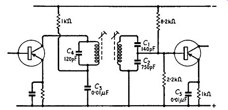
Fig. 8.10. A stage of a 10.7 Mhz i.f amplifier using drift transistors and
double tuned transformers required. A suitable value for the working Q. is
50. Thus, for the primary winding:
...and for resonance at 10.7 Mhz the tuning capacitance must be 120 pF.
To obtain a satisfactory i.f. transformer it is advisable to have an identical secondary winding also with an inductance of 1.8 µH and a tuning capacitance of 120 pF. This must be damped by the input resistance of the following transistor to give the desired working Q. of 50 and also to match the output resistance of the previous transistor to this input. The input resistance of the transistor is 150 ohms and to obtain the equivalent of 6 k-O connected across the whole of the secondary winding the transistor can be connected to a tapping point on the inductor, the turns ratio of the whole secondary inductor to the tapped part being given by:
Alternatively, as suggested in the circuit diagram of Fig. 8.10 the transistor can be tapped down the capacitive branch of the secondary circuit. The ratio of the two capacitances to give the required damping should be (6.3 - 1) : 1 i.e. 5.3 : 1. We thus require two capacitors for the secondary circuit whose ratio is 5·3 : 1 and which give a net capacitance of 120 pF. Their values can be calculated in the following way:
Substituting for C2 in the second equation:
These values and also other practical values of components required in a 10.7 Mhz i.f. amplifier stage are indicated in Fig. 8.10. A number of such stages are necessary to give the gain and selectivity required in an f.m. receiver and a description of a complete receiver using stages of this type is given in Chapter 11.
It was shown earlier that the gain of a 10·7 Mhz i.f. stage which feeds into the base circuit of a similar stage is approximately 20 dB. This is the gain obtainable from each of the i.f. stages in a receiver with the exception of the last which operates into the detector. The input resistance of a ratio detector can easily be 10 k-O and such a value permits gains approaching 100 from the previous amplifier. To show this we can use the general expression
. . gm2 TtTo maximum gam = 10 log10 -4
Substituting gm= 30 mA/V, r, = 10 kn, r0
= 6 k-ohm which apply when the previous stage is a drift transistor we have
. . 10 I (30 X 10-s)2 X 1Q4 X 6 X 10a dB maximum gam = og10 4
=41.3dB
The insertion loss of the tuned circuits will, of course, reduce this figure and a more practical value is probably 36 dB corresponding to a voltage gain of 65.
Decoupling
In Fig. 8.10, as in most of the circuit diagrams in this book, the source of base input signal (i.e. the secondary winding of the i.f. transformer) and the emitter decoupling capacitor are both returned to the positive terminal of the battery supply. This minimizes the impedance of the external base-emitter circuit which
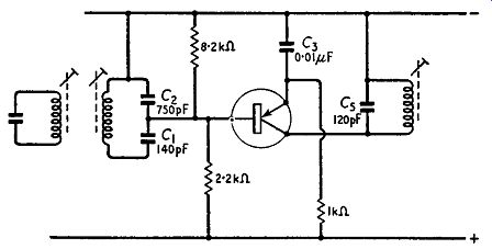
Fig. 8.11. A modified version of the wiring of Fig. 8.10 which eliminates
the need for collector decoupling components.
... is essential for maximum performance. The primary winding of the i.f. transformer must be returned to the negative terminal of the supply to provide the necessary collector bias but should be returned to the positive terminal of the supply in order to minimize the impedance of the external collector-emitter circuit which is also essential for best results. This difficulty is usually overcome by connecting a low-reactance capacitor C3 (the collector decoupling capacitor) between the primary winding and the emitter (or the positive terminal of the supply which is in turn connected to the emitter via the low-reactance emitter decoupling capacitor). If the collector decoupling capacitor is omitted, the signal output current of the transistor must flow through the impedance of the battery in addition to the primary winding of the transformer. In this way signal voltages are developed across the battery and these, if impressed upon other stages of the amplifier or receiver of which this stage is part, can distort the shape of the frequency response curve or even cause instability. To avoid this the collector de coupling capacitor C3 is included to short-circuit the battery at signal frequencies.
However, by a simple alteration to the wiring such a capacitor becomes unnecessary. If the source of base input signal (i.e., the secondary winding) and the emitter decoupling capacitor are both returned to the negative terminal of the battery supply, as shown in Fig. 8.11, then the impedance of the external base-emitter circuit and of the external collector-emitter circuit are both minimized simultaneously and no additional decoupling capacitor is necessary.