AMAZON multi-meters discounts AMAZON oscilloscope discounts
JUST as the amplifier stages of a receiver are invariably followed by a detector, so our discussion of amplification is followed by a consideration of detection. Detectors play an important part in radio receiving systems because they are required in order to reproduce the message which is transmitted by means of the radio-frequency carrier. Thus, it is the function of the detector to interpret the variations in the carrier amplitude in terms of the original message, whether it be code, music, speech, or a video signal. If the detector does its job perfectly, then its output is exactly similar to the original wave which was used to modulate the carrier. It is appropriate to mention here that this function of detection is also sometimes ref erred to as demodulation or rectification, and that the detector stage in a receiver is often called the demodulator stage.
The Diode Detector
One of the simplest and most effective types of detectors is the widely used diode. Since we have already considered the operation of the triode and other multi-element tubes in some detail, understanding the operation of the diode, which contains only a cathode and plate, is rather easy. Fig. 3-1(a) shows a simple diode circuit connected so as to bring out the essential properties of this two-element tube. As the characteristic in (b) of this figure shows, the electrons given off by the cathode are attracted to the plate when a positive voltage is applied. However, when a negative voltage is applied, the electrons are repelled and no current flows through the tube. Thus the diode has the fundamental property that it will conduct current in one direction only, and this only when the plate is positive with respect to the cathode. It is for this reason, of course, that the diode is called a rectifier tube.
Although we generally look upon the diode as a linear rectifier in which the current is proportional to the applied voltage, actually the diode current is not strictly proportional to the voltage as Fig. 3-1 shows. However, the characteristic can be …
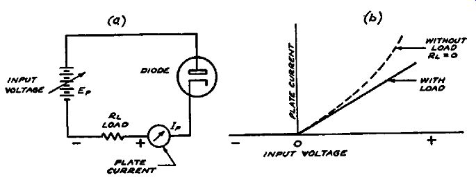
Fig. 3-1. A basic diode circuit is shown at (a). The use of a large value
of load resistance has a straightening effect on the plate current variation
as shown at (b).
... straightened out by using a large value of load resistance. As shown by the full line characteristic in Fig. 3-1 (b), the plate current variation becomes more and more closely proportional to the input voltage as the value of load resistance is increased. In all practical circuits which are used with the diode, especially in diode detectors, the load resistance is sufficiently high so that the plate current variation follows the input voltage exactly. In this way the possible introduction of distortion as the result of non linearity is avoided.
The input voltage, to which we have been referring and which is designated in the figure, should be carefully distinguished from the actual voltage which is applied between the diode plate and its cathode. Thus the input voltage is actually the voltage which is applied to the diode in series with the load resistance. When a load resistance is used, as is almost invariably the case in practical circuits, part of the input voltage appears across the load resistance and part appears across the diode. As the figure shows, the polarity of the voltage developed across the load resistor is such that the plate side of the resistor becomes negative as a result of the applied voltage.
Let us examine how the diode is used as a detector by considering the action which takes place when a modulated signal is applied to a typical diode circuit. Basically the circuit shown in Fig. 3-2(a) is similar to that used in the second detector of ...
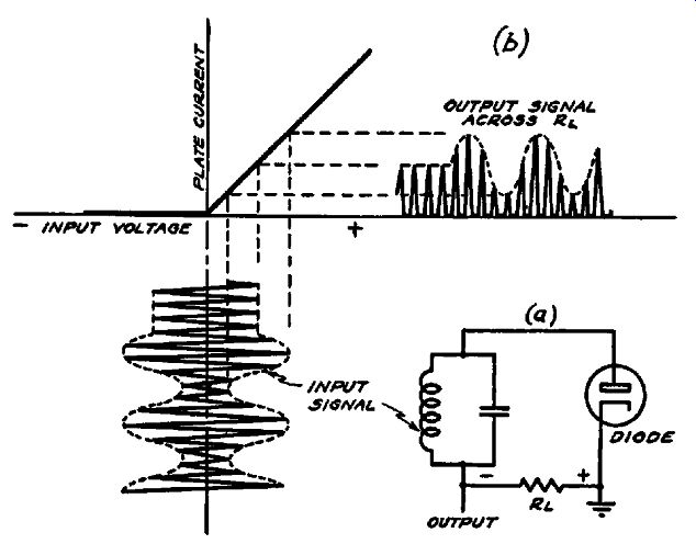
Fig. 3-2. A basic diode circuit is shown at (a). When a modulated signal is
applied to the diode input, rectification of the signal takes place as shown
at (b).
... receivers, but in order to simplify the discussion we have omitted a number of relatively unimportant features. Ref erring now to this figure, we see that the signal voltage, which for example might be that across the secondary winding of an i-f transformer, is connected in series with the diode plate and with the diode load RL. Of course, this signal voltage need not be an i-f voltage, it might just as well be at any other frequency, and in fact an action similar to that explained below would be obtained if the input voltage were at 60 cycles and the diode were a power rectifier such as the type 1-V tube.
To illustrate the action which takes place when a signal voltage is applied to the diode, we use the same type of representation which was employed in the preceding section in connection with amplifier tubes. Thus in Fig. 3-2 (b) we show the diode characteristic which is essentially a straight line because of the high value of load resistance. The input signal, which is a typical modulated wave, is shown below the plate current axis, and the corresponding variations in plate current caused by the application of the signal are clearly shown at the right. The manner in which the rectifying property of the diode is brought into play is clearly apparent. On the negative part of the signal cycle, the electrons are repelled from the plate and no current flows through the circuit. On the other hand, each positive part of the cycle causes a corresponding pulse of current to flow through the circuit and through RL. Thus the negative halves of the signal are removed and only the positive halves of the signal voltage are effective in causing current to flow through RL. As we pointed out above, the purpose of a detector is to produce an audio signal which follows the envelope of the modulated carrier. From the figure which we have been discussing, it is easy to see that the action explained above produces an output the average value of which varies in accordance with the modulated wave. However, along with this a-f signal accompanying the detection of the wave, we also have the r-f variations in the plate current. These variations are present across RL because no effort has been made in this simple detector circuit to eliminate them.
We shall see later that a number of different methods are used in receivers to remove the r-f or i-f pulsations of current from the diode load and to leave only the audio current. The example we have just shown is helpful in that it illustrates clearly the manner in which a modulated signal is rectified.
Speaking of signals, there are a number of interesting things about the voltage developed across the diode load and shown in Fig. 3-2. In the first place, as a result of the fact that the diode passes current only on the positive peaks of the signal, the voltage developed across RL contains a d-c component, in other words, there is a d-c voltage developed across RL. The polarity of this d-c voltage developed across the diode load is an important consideration because this voltage is often used as a control voltage in avc circuits. As in the previous illustration Fig. 3-1 where a steady voltage is applied to the diode, the plate side of the load resistor becomes negative with respect to the cathode side. Incidentally, this will always take place in every diode circuit no matter whether a d-c or an a-c voltage is applied to the diode. As a consequence of the fact that the diode will pass current in only one direction, that side of the load resistor which is closest to the plate will become negative and that side of the resistor closest to the cathode will become positive.
In addition to the d-c component of voltage produced across the diode load as a result of rectification, there are additional frequencies present across the load as we can easily see from an examination of Fig. 3-2. In the first place, the positive half cycles of the carrier which are rectified and appear across the diode load represent a strong signal at the intermediate or carrier frequency. Since this signal is distorted as a result of the elimination of the negative peaks, it contains many harmonics. In the case of the second detector in a superheterodyne, these frequencies, which we have just said existed across the diode load, would be the intermediate frequency and harmonics of the intermediate frequency.
Leaving these signals for the moment, we hasten to point out that in addition to (1) the d-c component, and (2) the carrier frequency and harmonics of the carrier frequency, there is also present across the diode load (3) the audio wave or more generally the low-frequency signal which corresponds to the modulation of the envelope. In practically all circuits where the diode is used as a rectifier and especially in the detector circuits used in receivers, the presence of the carrier signal and the harmonics of the carrier across the diode are undesirable. Thus in the second detector of a super heterodyne receiver, the presence of this strong i-f signal across the diode load would result in the i-f signal being fed into the a-f amplifier with resultant distortion, over loading, and the causing of numerous whistles.
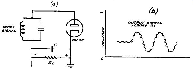
FIG. 3-3. A typical detector circuit using a condenser across the load is
shown at (a). The rectified output at (b) shows that this condenser removes
practically all of the carrier signal.
To eliminate the carrier frequency and its harmonics from the output of diode detectors, it is common practice in receiver de sign to by-pass the diode load with a condenser. As we show in Fig. 3-3, this condenser C offers a low-reactance path to the intermediate frequency, so that practically no r-f or i-f voltage is developed across the load. With this shunt condenser· across the diode load, the application of a signal voltage results in the production of a direct current through the load RL. Unlike the previous case where no condenser was used, the current in the diode circuit does not return to zero during each cycle, but instead the condenser C charges up to a value which is slightly less than the peak value of the carrier signal. As the figure shows, when the carrier is unmodulated so that its amplitude does not vary, the plate end of the load resistor is maintained at a constant negative voltage with respect to ground. When the carrier amplitude varies, as it does when the signal is modulated, the pulsating output follows the modulation in the manner indicated in Fig. 3-3 (b). In this way an audio output is produced which has the same waveform as the envelope of the modulated signal.
No doubt you have noticed the ripple in the voltage present across RL in Fig. 3-3 (b). This indicates the fact that the con denser C does not remove all of the i-f signal from the diode load but that a small amount of the carrier is still left across the load.
This slight ripple is due to the fact that the diode plate draws a charging current into the condenser only for a very small interval at the positive peak of the cycle. During the remaining parts of the cycle, the steady negative voltage across RL makes the diode plate negative with respect to the cathode and thus prevents the diode plate from drawing current. Later in this section, in examining the application of signal tracing to diode circuits used in receivers, we shall examine several widely used filter circuits to further reduce the extent of the carrier ripple across the diode load. We might point out, however, that even without additional filtering, the amount of carrier signal which is left across the diode load is not usually sufficient to interfere with the operation of the receiver. This is especially true because the i-f signal will not be amplified by the a-f amplifier since the latter does not amplify at frequencies well above the audio range.
It may have occurred to you that a large condenser might be used across the diode load in order to remove the i-f signal completely from the diode load. Actually, however, the value which is used for this condenser is a sort of compromise value which is arrived at by taking into account the following facts. On the one hand the value of this condenser should he high so that the carrier frequency will be removed from the output of the diode. On the other hand, though, if this condenser is made too large it will by-pass the higher audio frequencies, and decrease the high frequency response of the receiver by acting in a manner similar to a tone control. Thus the final value of this condenser is the result of taking into account these two factors. An additional factor which is considered by design engineers is the fact that a large value of condenser decreases the ability of the detector to handle high values of percentage of modulation without distortion.
Typical Diode Detector
We are now in a position to examine a typical diode detecto1· circuit and to look into the distribution of signals throughout the circuit. The circuit shown in Fig. 3-4 is in general similar to the preceding circuit, but appears more complicated because of several additional components. However, basically the action taking place in the two circuits is the same. Let us examine these additions which we have just mentioned. You will note that the volume control is the d-c diode load and that the amount of audio signal which is picked off and fed to the a-f amplifier is controlled by the setting of R2. At all times regardless of the setting of the volume control, the full value of a-f signal voltage is developed across R2. An additional filter has been added in series with the diode load. This consists of the resistor R1 and the condensers C1 and C2. The purpose of this filter is to remove the i-f component of the signal more effectively so that only a comparatively small i-f signal will be present across the audio volume control. In addition to improving the filtering of the i-f signal, this filter combination also helps to improve the fidelity of the detector for signals having a high percentage of modulation.
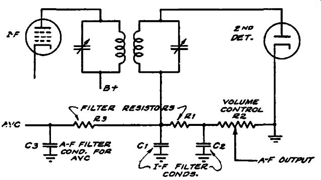
Fig. 3-4. A typical diode detector showing the a-f and avc output circuits.
One of the reasons for the wide popularity of the diode in modern receivers is that its use simplifies the production of a control voltage for use in avc and other control circuits. These will be discussed in detail in the section on control circuits. For the present it will suffice to say that the negative voltage produced by the direct current flowing through R1 and R2 is suitable for avc purposes since its value is proportional to the carrier amplitude. Since, as we have seen, both d-c, a-f, and i-f signals are present across the diode load, the filter R3-C3 is used to remove the a-f and i-f components from the avc voltage and to leave only the d-c control voltage.
Contact Potential
In connection with the d-c voltage developed across the diode load by the presence of an input signal, we should mention that there will always be a small negative voltage present at the diode plate and of course at the plate side of the diode load. This voltage which is often called the "contact potential" is produced by the electrons which leave the cathode with sufficiently high speed to reach the plate. For the average diode tube, such as that contained in the 6H6 and similar tubes including dual-diode triode types, this contact potential has a value of about minus one volt under typical circuit conditions. An interesting characteristic of this contact potential is that its value depends upon the diode load resistance and the higher the value of load resistance the higher is the value of the contact potential. Thus, when the diode is open circuited and the voltage at the plate is measured with a high-resistance voltmeter, the contact potential will measure about - 1 volt. For a load resistance of about 100,000 ohms, the diode potential will drop to a few tenths of a volt. Finally the voltage at the plate will drop rapidly to zero as the load resistance is decreased further. When troubleshooting, you should remember that this negative voltage normally exists across the diode load and that it does not indicate the presence of a signal.
Full-Wave Detector Circuit
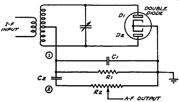
Fig. 3-5. A full-wave detector circuit using a double diode such as a 6H6.
The distribution of signal voltages is described in the text.
The detector circuits described up to this point have all been half-wave rectifier circuits since only one half of the carrier wave is rectified. In contrast to these half-wave detector circuits, we show in Fig. 3-5 a full-wave rectifier or detector circuit which has been used rather widely in receiver circuits. If you examine this circuit closely, you will observe that it is similar to the type of full-wave rectifier circuit used in practically all receiver power supplies, with the filter choke omitted and R1 serving as the load circuit.
From the viewpoint of signal tracing, the full-wave detector circuit has several interesting characteristics. First of all, we note that both halves of the input signal are rectified since each of the diodes draws current on alternate halves of the cycle.
Thus on that half of the cycle where D1 is positive, this diode draws current and contributes a pulse of current through the diode circuit. During this interval D~ is of course not drawing current because the other half of the center-tapped input winding is negative. During the next half of the cycle, the plate of D2 is positive with respect to its cathode; thus it contributes a pulse of current through the load in the same direction as the current passed by the first diode on the preceding half cycle.
In this way both halves of the input signal are rectified, each of the diodes functioning exactly as in the case of the preceding half-wave detectors. The resultant output is thus similar to the wave shown in Fig. 3-3(b), with the exception that the frequency of the carrier ripple is twice as great because of the full-wave action.
Because of the balanced nature of this circuit there is no i-f signal voltage at the center-tap of the secondary winding of the input circuit. However, harmonics of the i-f or carrier frequency are present across the diode load. These, however, are not important and their presence is ordinarily of no consequence.
Actually, it is not possible to achieve perfect balance so that in commercial receiver circuits a small by-pass condenser will generally be found across the diode load. Even where the circuits are perfectly balanced, this condenser is useful because it serves the purpose of by-passing the harmonics of the carrier frequency which are always present across the diode load.
The full-wave circuit shown in Fig. 3-5 shows an interesting variation in that the volume control is located so that the d-c component of the diode current is blocked from the volume control by means of the condenser C2. In practice, C2 is large enough so that the audio frequencies developed at point 1 will be fed to point 2 and develop essentially the same value of audio voltage at point 2. A tendency toward longer volume control life and greater freedom from noise has been found to be characteristic of this type of circuit in which the d-c component of the diode current does not flow through the audio volume control.
Capacity-Coupled Diode
The diode circuit shown in Fig. 3-6 is often used as a detector but more especially as a rectifier for supplying control voltages.
The essential feature of this circuit is that the signal voltage is ...
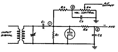
Fig. 3-6. A capacity coupled diode detector circuit. The operation and signal
distribution are discussed in the text.
... coupled into the diode circuit by means of a condenser. As a result, the rectified d-c component of the diode current cannot flow through the tuned circuit which generally supplies the signal voltage. This of course is a consequence of the general principle that no direct current can flow through a condenser.
When a signal is applied to the tuned input circuit, this signal voltage is impressed on the plate of the diode. Thus the signal voltage at the plate of the diode is essentially the same as that across the tuned circuit. On the positive peaks of the signal voltage cycle, electrons are attracted to the diode plate and this rectified current flows through the diode load resistor R1. You can look upon the action taking place as one in which a circulating rectified current flows through the closed circuit consisting of the diode and the load resistor R1. As in the previous diode rectifier circuits, this current causes the plate side of the load resistor to become negative with respect to ground, and also causes the demodulated or a-f signal voltage to appear across R1.
No doubt by this time you have noticed that no by-pass condenser is used across the diode load R1 as in the previous circuits. It is not difficult to see why this is so. In the other circuits, for example that of Fig. 3-3, the action of the circuit did not depend upon the existence of the i-f or carrier signal voltage across the resistor and thus it was both possible and desirable to by-pass this voltage. However, in the present circuit the signal voltage must be impressed across the diode by means of the signal voltage drop across Rt so that this signal voltage cannot be by-passed. If a condenser were used across Rt, on the other hand, then this would have the effect of by-passing the signal voltage, and thus make the circuit inoperative.
An important point in understanding the action of this circuit and one that is often misunderstood is that the diode does not act as a partial short circuit across the input during the interval that the diode is conducting current. Although the diode does have a low internal resistance of approximately 2000 ohms while it is passing current, still this 2000 ohms does not load the input circuit because whatever current is drawn by the diode passes through R1 and is limited by this high value of load resistance.
Thus the loading is determined not by the low internal resistance of the diode, but rather by the value of R1.
As is indicated in Fig. 3-6, the capacity-coupled diode can be used to supply avc voltage and it is often used for this purpose as well as to supply other types of control voltages. To obtain the control voltage produced by the d-c component of the diode current, it is general practice to use a filter similar to R2 and CS. Since R2 effectively shunts the input circuit, its value is generally of the order of a megohm in order to minimize loading. The value of C2 is sufficiently large to remove the audio pulsations from the output circuit and its value will generally be of the order of 0.05 mf.
When the capacity-coupled diode circuit is used to supply audio voltage, the load resistor across which the audio voltage is developed is generally coupled to R1 by means of a filter R3-C3. The values of R3 and C3 are sufficiently large so that the carrier frequency is kept out of the volume-control circuit and so that the capacity of the volume control does not detune the circuit.
Note that with this circuit it is not possible to obtain the full audio voltage across the volume control since part of the audio signal is lost across the filter resistor RS. For example, in the particular case where R3 and R4 are equal, then one half the full audio output is available at the volume control.
With reference to the signal distribution in this circuit, at point 1 will be found both the i-f signal and its harmonics, as well as the audio signal, and the negative control voltage. At point 2, however, both the i-f signal and the audio signal are filtered, and only the negative control voltage is present. At point 3, across the volume control, both the negative voltage and the audio signal are present, but of course the full output voltages which were present at 1 are not obtained because of the voltage divider action produced by R3 and R4. Only a small fraction of the carrier signal is present at point 3 because of the filtering action of R3-C3. We might point out here that triodes are sometimes used as diodes in receiver circuits by connecting two of the elements together to form a two-element tube. In some cases the triode plate is connected to the cathode and the grid forms the other element of the diode. In other cases, the grid and plate are tied together to form the diode plate, while the other element is formed by the cathode. Where triodes are used in this way as diodes, everything which we have previously said about diodes may be taken as applying to these tubes. Thus, for example, any one of the circuits which has been discussed, or in fact any circuit in which a diode can be used will also function with a triode connected as a diode.
The application of various types of diode circuits to perform different functions, and employing circuit arrangements some what different from those considered, is reserved for later discussion in the sections devoted to the types of radio circuits. We are here referring to double diodes used in automatic-frequency control systems, discriminator circuits, amplified delayed avc circuits, noise suppression circuits, limiting circuits, etc.
TRIODE AND MULTI-ELEMENT DETECTORS
While the diode detector is the most widely used detector in modern receivers, there are a number of other detector circuits using multi-element tubes which should be discussed in this book.
For the most part these detectors were used in early receivers, but since many of these receivers are still in use, it is worthwhile considering multi-element detectors in some detail. We do not want to create the impression that none of the detector circuits to be described is used in current receivers; in many cases we find that triode and screen-grid detectors are still being used where they are better adapted than the diode to the requirements of particular receivers.
If we examine the various types of detector circuits, we find that they all have this in common: they depend for their operation upon the curvature or bend in the tube characteristic. With out exception we find that the operation of all types of detectors is predicated upon the operation of the tube so that it conducts current better in one direction than in the other. In the case of the diode, we saw that this simple tube is ideally suited for detection because complete rectification is obtained, i.e., on one half of the cycle current was passed and on the reverse half of the cycle no current whatsoever was passed. In the case of the triode and other multi-element detectors, we find as a general rule that the rectification is not so simple as in the case of the diode but that some current is generally passed by the tube on the negative half of the cycle. However, in every case, the current passed on the positive half of the cycle exceeds that passed on the negative half of the cycle so that detection is obtained.
As you read this section, you will note the great similarity between diode and multi-element detectors. True, the triode and screen-grid detectors are somewhat more complicated because the process of amplification is combined with that of detection.
Nevertheless these detectors have much in common with the diode detector, especially from the viewpoint of signal tracing.
Thus we shall see, for example, that the manner in which the carrier signal is removed from the detector load, and the distribution of signals, is much the same for multi-element detectors as for diodes.
The Linear or Plate Detector
Perhaps the most widely used of the multi-element detectors is the circuit shown in Fig. 3-7 which uses a triode tube. This type of circuit is known by a great many names among which are linear detector, plate detector, grid-bias detector, anode detector, and power detector. However, regardless of the name which is used to describe this basic detector circuit, it is important to be able to recognize the circuit when you meet it. As you can see from Fig. 3-7, the circuit shown is very similar to that of an amplifier stage and in fact with the exception of Cf, which is identified as the plate by-pass condenser, it is identical with that of a resistance-coupled amplifier stage. Because of this similarity we should expect that the operation of this circuit would have much in common with the operation of an amplifier stage, and actually such is the case.
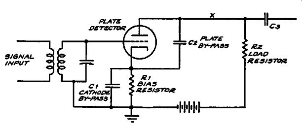
FIG. 3-7. A basic circuit for plate detection showing the function of the
various parts.
Although the plate detector circuit shown in Fig. 3-7 shows this marked similarity to a resistance-coupled amplifier stage, actually the action which takes place when a signal is applied to the stage is different. This is because the detector stage, which we are discussing, is biased almost to plate-current cut-off or to zero plate current. On the other hand, in an amplifier stage the bias is set so that the signal will cause the plate current to vary by an equal amount on each side of the steady plate current. An examination of Fig. 3-8 will show you the contrast between the two types of operation. When the triode is used as an amplifier, as in Fig. 3-8 (b), the bias and operating conditions are set so that the operating point is in the middle of the straight part of the plate current characteristic. On the other hand, when operation as a detector is desired, the grid bias and other conditions are adjusted so that the plate current is reduced almost to zero; this is shown in Fig. 3-8(a).
We need not go into a lengthy description of the circuit in Fig. 3-7 because we have already discussed diode detectors and triode amplifiers. Referring to this figure, we note that just as in the triode amplifier, the input signal is applied between the grid and ground so that this constitutes the input circuit. In the cathode circuit the resistor R1 supplies the proper bias so that the plate current is practically cut off when no signal is applied. In actual practice, the no-signal plate current for biased triode detectors is usually of the order of 0.2 milliampere. We note that the cathode resistor is by-passed by the condenser C1. Because both the carrier signal and the demodulated or audio signal developed as the result of rectification is present at the cathode, C1 is generally of the order of a microfarad so that it will by-pass not only the carrier frequency but also the lower audio frequencies.
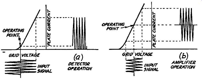
Fig. 3-8. A tube operated as a detector has its operating point near cut
off, whereas in amplifiers the operating point is in the middle of the straight
part of the characteristic.
In the plate circuit, we encounter a somewhat different situation. Here the audio voltage is developed across the load resistor R2. However, the by-pass condenser C2 must be sufficiently small so that it will not by-pass the audio frequencies back to the cathode and in this way prevent the development of the audio signal across the load R2. On the other hand, C2 must be sufficiently large so that it will by-pass the r-f or carrier component of the plate current and prevent this carrier signal from being developed across the load. The presence of a carrier signal across the load would of course be undesirable because it would result in r-f voltage being fed into the a-f amplifier. In addition to this factor, it is necessary to have CS by-pass the carrier signal in order to prevent amplification of the carrier signal from interfering with the action of the tube as a detector.
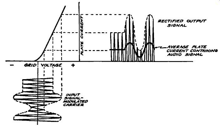
Fig. 3-9. The plate-current variations in a triode biased near cut-off, when
a modulated carrier signal is applied to the grid, are shown.
We can describe the action which takes place in the circuit when a signal is applied by the same method which we used in analyzing the action of the triode amplifier. In Fig. 3-9 we show the plate current-grid voltage characteristic of the triode and the resultant variation in the plate current which takes place when a modulated signal is applied to the grid. On the positive half of the input cycle we note that a very large increase in the plate current of the triode takes place. On the other hand, because the tube is biased very near cut-off, only a slight decrease in plate current can take place during the negative half of the cycle. Thus we have detection taking place just as in the case of the diode, and we find that the plate current through R2 of Fig. 3-7 varies in accordance with the amplitude of the modulated input signal.
In this way, the average plate current causes an audio signal voltage to be developed across R2.
Generally speaking the rectifying action which we have just described is very similar to that which takes place in the diode.
However in this case the rectifying action is accompanied by amplification so that a considerably greater output is obtained from a triode detector than from a diode, for the same value of input signal. This accounts for the wide use of the triode detector in the early receivers since at that time r-f amplification was difficult and expensive to obtain. Thus the additional sensitivity which could be obtained by using a triode detector was very helpful.
The distribution of signal voltages in triode circuits is very similar to that in diode circuits, bearing in mind of course that with the diode no amplification is obtained, whereas with a triode both detection and amplification of the output are obtained at the same time. At the control grid of the tube we find that only the input signal is present; this may be either the r-f signal in the case of a tuned r-f receiver or the i-f signal in the case of a superheterodyne receiver. Naturally there is no a-f signal present at this point since rectification does not take place in the grid circuit. On the other hand, you will remember that in the case of the diode detector not only the input r-f signal was present at the diode plate, but the d-c output and the a-f output as well.
At the plate of the triode we find that the a-f signal is present.
This signal is considerably stronger than would be the case for a diode because of the amplification which is obtained. A relatively weak component at the carrier frequency is also present at the triode plate because of incomplete filtering.
At the cathode we find that normally no signal is present be cause the cathode by-pass condenser is made large enough so that it will by-pass both the carrier and the a-f components of the plate current. However, it is worthwhile mentioning that the d-c bias voltage across the cathode resistor R1 increases as the carrier input signal is increased. The rated value of bias voltage which is given in the service notes is ordinarily the value with no input signal.
There are a great many variations from the basic triode detector circuit which we have just described. Fortunately, many of these have already been covered in connection with amplifier operation so that we shall not have to go into detail here. Thus, for example, the circuit shown in Fig. 3-7 uses a cathode resistor to supply the proper bias for the tube. But the other systems used in amplifier stages to obtain bias can also be used with det4lctors and so we find that a bleeder circuit, or battery bias in the case of battery-operated receivers, can be used to supply the bias required to reduce the plate current to cut-off.
Although we have shown the triode detector with a resistor for the plate load, this type of detector is often used with transformer coupling as well as with resistance coupling. In this connection, we have already described transformer-coupled amplifier stages so that further discussion of the transformer-coupled detector is unnecessary. However, the transformer used with a detector stage is different from that used with a transformer-coupled a-f stage even where the same tube type and plate voltage is used in both cases. This is because the triode operated as a detector has a higher plate resistance so that the turn ratio and input impedance are generally higher for the detector transformer. Distorted operation will usually result when an interstage a-f transformer is used to replace a detector output transformer.
Several different types of filter arrangements are used to reduce the level of the carrier signal at the plate of the detector tube.
In Fig. 3-7 a by-pass condenser is used to by-pass the signal back to the cathode. Sometimes this condenser is returned directly to ground but this does not change the by-passing action because the cathode is by-passed to ground by means of C1. Very often where more effective filtering is required, an r-f choke is inserted at X in Fig. 3-7. This r-f choke has the effect of blocking the carrier currents from the load circuit so that only the a-f signal will be developed across the load. Where this r-f choke is used, it is customary to use an additional by-pass condenser on the load-resistor side of the choke in order to increase further the effectiveness of filtering. Of course the value of both of these condensers is small in order to prevent the loss of the higher audio frequencies.
Tetrode and Pentode Detectors
The biased detector circuit which has just been described is used with screen-grid tubes as well as with triode tubes. When the screen-grid tube is used as a detector, it is adjusted so that the plate current is practically cut off and as a result rectification of the modulated input signal and detection is obtained. Thus we can use the same figure that was used in the case of the triode to describe the effect of the input signal on the plate-current variation through the detector load. The essential point to keep in mind is that in order to obtain detection, the tube must be adjusted so that the increase in plate current on one half of the cycle will be greater than the decrease in current on the other half of the cycle. Whether the tube is a diode, triode, tetrode, or a pentode, makes no difference in this basic requirement for detection.
Because of the greater amplification possible with the screen grid tube, it is much more sensitive as a detector than the triode.
In addition to the greater sensitivity as a result of the higher amplification, the efficiency of detection is greater for the screen grid type because of the sharper cut-off which it is possible to obtain in tetrode and pentode tubes. This is especially true of the so-called "sharp cut-off" types where the plate current drops very sharply to zero. Tubes similar to the 57, 77, 6C6, and 6J7 types are examples of sharp cut-off tubes which are often used as biased detectors.
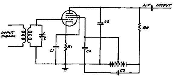
Fig. 3-10. A typical biased detector circuit using a pentode tube.
A typical biased detector circuit using a pentode tube is shown in Fig. 3-10. Again, as in the case of the triode, we need not discuss this circuit at length because of its similarity to the pentode resistance-coupled amplifier. Thus the screen voltage is supplied from the tap on the voltage supply and is by-passed for both r-f and a-f currents by means of the condenser C4. Similarly, the cathode resistor R1 is also by-passed by means of the condenser C1. Since a-f as well as r-f currents flow through the cathode resistor, C1 is generally made large enough so that it will by-pass the lower audio frequencies. The suppressor grid does not require any special attention since it is usually connected to the cathode of the tube at the socket.
Because of the high value of load resistance required for the proper operation of screen-grid detectors, resistance coupling is almost invariably used. On the other hand, transformer coupling is of ten used with triode detectors but practically never in receivers with screen-grid detectors. In general the voltages used in screen-grid detector circuits are similar to those used in resistance coupled screen grid a-f stages. However, because operation at cut-off is desired, the grid-bias used is larger than that used in amplifier stages.
The introduction of the screen grid does not change the signal tracing procedure appreciably, but it does provide an additional tube element which must be taken into account. Normally, the by-passing action of C4 will be sufficient to prevent the building up of an a-f signal at the screen grid of the tube so that no signal voltages will be present at this point unless C4 is open. Signal tracing at the remaining points remains exactly the same as for the triode detector so that no additional comments are required.
The Grid-Leak Detector
Practically all receivers more than twelve years old employ a detector circuit which is somewhat different from any that we have described so far. This is the so-called grid-leak detector which was widely used in early receivers because of its high sensitivity on weak signals. In those days it was not possible economically to build amplifiers which provided high gain in the r-f end of the receiver and consequently a detector which was sensitive to weak signals was very desirable.
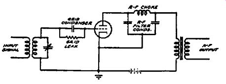
Fig. 3-11. A typical grid-leak detector. Bias is supplied by the rectified
grid current through the grid leak.
The circuit which we show in Fig. 3-11 is typical of grid-leak detectors. These circuits are easy to recognize because practically without exception they were used only in early receivers and are now no longer in common use. Unlike the grid-bias detector, the grid-leak detector is operated at zero bias and the grid is returned directly to the cathode through the grid-leak and the tuning coil. Since the coil resistance is only several ohms, whereas the resistance of the grid leak is of the order of megohms, the coil resistance is not of importance. As a matter of fact, in some cases the grid leak is returned from the grid directly to the cathode, but this does not alter the operation of the circuit.
To understand the operation of the grid-leak detector, it is convenient to consider that the grid-cathode sections of the tube form a diode and that the grid leak and grid condenser constitute the load for this diode. Thus, when a signal is applied to the input circuit, this signal voltage is fed to the grid through the grid con denser which has a low reactance to the carrier frequency. Exactly as in the case of the diode, a rectified voltage is developed across the grid leak and this negative voltage is applied directly at the grid of the tube. An essential feature of the circuit is the operation of the tube at zero bias, and also the operation of the plate at a low d-c voltage. Both of these factors combine to make the grid-cathode circuits of the tube act as a rectifier, in which the grid acts in a manner similar to the plate of a diode. Once the audio voltage is developed at the grid by the signal, it is amplified by the triode action of the tube and the resultant audio output appears across the primary winding of the transformer.
It is interesting to contrast this action with that in the biased triode detector. For the biased detector, we saw that the application of a signal caused rectification to take place in the plate circuit, and as a result the average plate current increased when a signal was being received. In the case of the grid-leak detector, however, the application of a signal causes a negative voltage to be developed at the grid, and thus rectification in the grid circuit causes the average plate current to decrease. The amount by which the average value of the plate current decreases of course depends upon the carrier level, and for this reason the current flowing through the primary winding of the output transformer follows the envelope of the modulated signal.
The signal distribution in the grid-leak detector is different from that in the biased detector because of the presence of the a-f signal at the grid of the tube. In this connection, the grid con- denser is made sufficiently small so that it will not short circuit the higher audio frequencies and prevent the audio voltage from being built up at the grid. No discussion of the signals present in the plate circuit is required since this has already been described for the biased detector and is the same for the grid-leak detector.
The grid-leak detector has the disadvantage that it will easily overload even on medium signals and also that the percentage of distortion in the output is higher than for the other types of detectors which we have discussed. In addition, the loading on the input tuned circuit is considerably higher because current is drawn in the grid circuit, whereas in the other circuits (with the exception of the diode) rectification takes place in the plate and not in the grid circuit.
Infinite-Impedance Detector
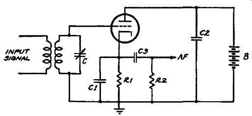
Fig. 3-12. A typical infinite impedance detector circuit. The audio output
is taken off between the cathode and ground.
A few years ago a new detector circuit was introduced to enable obtaining many of the advantages of the diode circuit without the loading effect characteristic of the diode. This circuit is known as the "infinite-impedance detector" and we show it in schematic form in Fig. 3-12. The most striking thing about this circuit is that the demodulated output is taken off between the cathode and ground, although the input circuit is between the grid and ground. In this respect the circuit is not unlike a widely used phase-inverter circuit which is arranged similarly.
With respect to the circuit, we note from the figure that the plate of the triode is by-passed to ground by means of C2. The value of C2 is sufficiently large so that both r-f and a-f currents are returned to ground and consequently there is no signal voltage of any kind at the plate of the tube. On the other hand, these signal currents must flow through the cathode resistor R1 in order to get back to the cathode so that a signal voltage is built up across R1. As in the case of the diode detector, the value of C1 is chosen so that only the r-f currents will be by-passed and consequently there will be practically no signal voltage at the carrier frequency between cathode and ground. However, the demodulated or audio voltage will of course be available between the cathode and ground because C1 is sufficiently small so that it will not by-pass the a-f signal.
In operation, the bias developed at the cathode is sufficiently high so that no grid current will flow when a signal is applied to the grid. This is true even for large values of input signal of the order of 30 volts and as a matter of fact the infinite-impedance detector is ordinarily designed for use in receiver circuits where a high value of signal voltage is available at the detector. In addition to this advantage that no grid current is drawn and that there is no loading on the input tuned circuit, the infinite impedance detector has the additional advantage that the distortion in the output is lower than it is for the diode. This is especially true for signals which have a high percentage of modulation. Of course, the infinite-impedance detector has the disadvantage that it cannot be used to supply avc voltage in the simple and direct way that the diode can.
Diode and Multi-Element Detectors
Now that we have described the various types of detectors, it is interesting to investigate just why the diode detector is so widely used in present-day receivers while the multi-element detectors find very little application. Among the principal factors which account for the widespread use of the diode is the fact that improved tubes and circuits have made possible high gain in the r-f and i-f sections of receivers, so that high sensitivity in the detector circuit is no longer required. In addition the output of the diode detector has a very low percentage of distortion and it will function satisfactorily over a wide range of input voltages.
Multi-element detectors, on the other hand, have higher distortion and require that the input signal be held within fairly close limits.
The development of effective avc circuits, however, has minimized the importance of this last factor since most receivers are designed so that the signal at the detector will have a fairly constant level regardless of the strength of the received signal. Last, but by no means the least important reason for the use of diode detectors is the widespread use of automatic volume control and the fact that the diode is so well adapted to supply control voltage for avc circuits.