AMAZON multi-meters discounts AMAZON oscilloscope discounts
6-1. Rectifier Required for A-C Voltage-Measuring Function of a VTVM
Almost all present-day vacuum-tube voltmeters are basically d-c voltage-indicating devices. As shown in Fig. 6-1, the d-c voltage to be measured (or a definite fraction of it selected by the d-c voltage-divider network) is applied to the input-grid circuit of an amplifier-type d-c bridge circuit. The bridge-potential unbalance produced by the application of this voltage causes current to flow through a conventional moving-coil type d-c microammeter. Consequently, when a-c voltage is to be measured, it must first be rectified so that it may be applied as d-c voltage to the voltage divider and d-c metering circuit of the vtvm. The meter scales are calibrated to indicate in terms of the magnitude of the a-c voltage. Use of a rectifier that produces linear rectification is preferable, so that the d-c meter indication will be directly proportional to the magnitude of the a-c voltage, and linear scales will result.
6-2. Typical Rectifier Arrangements Employed
Two types of rectifiers are employed; these are the vacuum-tube diode and the crystal diode. Although the application principles are the same for each type, each possesses certain advantages and disadvantages for specific applications.
Several rectifying circuits, and several arrangements of them with respect to the d-c indicator portion of the vtvm are in use. Their choice is influenced mainly by the waveform and the frequency of the a-c voltages that the combination will be called upon to measure. A review of the typical rectifier bridge circuit arrangements most widely used in modern vtvm's will be helpful here, before proceeding with the detailed study of the circuitry and operating characteristics of the various forms of rectifiers employed.
A simple half-wave (diode) rectifier arranged in a peak-indicating type rectifying circuit is usually employed in the peak-indicating type of vtvm's whose a-c voltage-measuring function is intended mainly for measurement of the peak values of any waveform, or the rms values of sine wave voltages only. This rectifier precedes the d-c voltage divider of Fig. 6-1, in the circuit. Another voltage divider (usually an a-c frequency-compensated type) may or may not be provided ahead of the rectifier to reduce high a-c input voltages under measurement to a value within the maximum voltage rating of the diode.
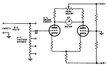
Fig. 6-1. Voltage divider, and simplified version of basic amplifier-type
d-c bridge metering circuit of a vtvm. This is the d-c voltage indicator. When
a-c voltage is to be measured, it must first be rectified so that it may be
applied as d-c voltage to the input terminals of this circuit. Several types
and arrangements of rectifiers are used with modern vtvm's; the choice is influenced
mainly by the waveform and the frequency of the a-c voltage that is to be measured
(see Fig. 6-2 and 6-3).
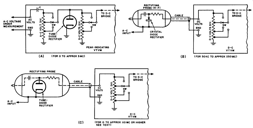
Fig. 6-2. Typical rectifier arrangements employed with peak-indicating type
vtvm's. (A) Built-in tube-diode rectifier. Used for low and medium-frequency
a-c voltage measurements. (B) Crystal diode rectifier, arranged in the form
of an accessory exterior probe, used for high-frequency a-c voltage measurements
to approximately 250 mhz. (C) Alternate type of probe rectifier that employs
a diode tube.
The rectifying circuit and the a-c voltage-divider may be built in as an integral part of the vtvm, as illustrated in Fig. 6-2A. One widely used vtvm that employs this rectifier arrangement has a rated frequency response flat to approximately 3 mhz, which includes power-line, audio, supersonic, and radio-frequency voltages up to the medium-frequency band. For measurement of sine-wave a-c voltages of higher frequency, with an accuracy of ± 10 percent from 50 khz to approximately 250 mhz, a calibrated half-wave germanium crystal-diode rectifier built into the form of exterior probe is used. This is attached to the instrument cable at the point of test, as shown in Fig. 6-2B. It is connected to the D-C Volts input terminals of the vtvm, so that the rectified voltage is then measured the same as d-c voltages. Observe that when this rectifying probe is used, it takes the place of the low-medium-frequency built-in rectifier shown in Fig. 6-2A. Another version of the peak-indicating vtvm arrangement of Fig. 6-2A is illustrated in part C of the same figure. Here, the frequency range over which accurate voltage measurements may be made is increased by arranging a calibrated vhf type tube-diode rectifier in an exterior probe at the point of test.
Accurate measurement of peak and rms values of sine wave voltages of frequencies up to approximately 110 mhz, and useful voltage-presence indication (not measurement) of voltages up to 300 mhz, is achieved in some popular-priced versions of this arrangement. (Such voltage-presence indication is useful in signal tracing work when it is necessary only to determine the presence, absence, or relative magnitudes, of a signal at certain test points in the equipment under test.) By employing a special probe construction and a special uhf type of diode, one vtvm (Hewlett Packard 410A) which uses this arrangement is rated to provide accurate a-c voltage measurement to 700 mhz, and useful voltage-presence indication to 3,000 mhz.
Some vtvm's are designed especially to indicate directly the peak-to-peak voltage values of sine waves and also of all complex waveforms and recurrent pulses such as are present in various circuits in television, radar and other pulsed electronic systems. In tv receivers, the voltages usually measured range in value from about 1 volt p-p at the video-detector load resistor to over 1,200 volts p-p at the horizontal-deflection coils. The peak-to-peak indicating vtvm is particularly useful in tv receiver service work because service manuals and notes for tv receivers usually include illustrations of the correct waveforms that should exist at many specified points in the circuit, and these illustrations are frequently labeled with the correct peak-to-peak voltages. The latter are useful for reference when making checks with a vtvm, since receiver faults that alter the voltage waveform usually also alter its peak-to-peak value appreciably. Separate scales are also provided for indicating directly the rms values of sine waves only.
Peak-to-peak vtvm's usually employ a voltage-doubler type of rectifying circuit that is either built into the instrument case as shown in Fig. 6-3A, or is contained in a separate probe as shown in part B of the same figure. The frequency range over which accurate voltage measurement is possible with the former arrangement ordinarily extends to approximately 3 me; that of the latter arrangement to approximately 110 mhz, although it may usually be used up to about 300 mhz for a-c voltage-presence indicating (not measurement) purposes in signal-tracing work.
Some service-type vtvm's which use the arrangement in Fig. 6-3A, for example the RCA Master and Senior Volt-Ohmysts, also make it possible to employ an accessory calibrated crystal-diode rectifying probe instead to provide peak indicating operation over the extended usable frequency range to approximately 250 mhz. This is connected to the D-C Volts terminals of the vtvm, as shown in Fig. 6-2B, so that it feeds directly into the d-c voltage divider and thence to the d-c bridge circuit. A calibrated high-frequency type of tube-diode rectifying probe, as illustrated in Fig. 6-2C, is used instead with some vtvm's, for this purpose.
Another rectifier arrangement of technical interest, illustrated in Fig. 6-3C, is used in the Hickok 209A vtvm and is explained in the caption. By means of this single exterior rectifying probe, with its unique switching arrangement located inside the vtvm, direct measurement of the peak-to-peak voltage value (up to 300 volts) of complex waveforms, and direct measurement of the rms value (up to 300 volts) of sine-wave voltages, over a frequency range to 100 mhz, with useful voltage-presence indication to 300 mhz, is obtained. A 4-wire cable is used between the probe and the vtvm, as shown.
6-3. Operation of the Shunt Type, Peak-Indicating, Tube-Diode Rectifying Circuit
Peak-indicating type vtvm's which use a tube-diode as the rectifier for a-c voltage measurements usually employ this in a shunt diode rectifying circuit (so named because the diode is shunted across both the input and the load circuits). The resulting d-c output voltage is applied to the d-c voltage divider of the vtvm, from which a definite fraction of it is applied to the input circuit of the amplifier-type d-c bridge circuit in the vtvm, as shown in parts A and C of Fig. 6-2. It is the function of the rectifier and the associated filter circuit to deliver smooth d-c output voltage that is proportional to the peak value of the applied sine-wave a-c input voltage. A disassembled tube-diode rectifier in probe form is illustrated in Fig. 6-4.
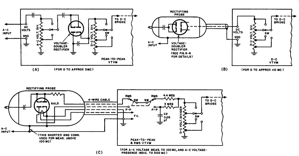
Fig. 6-3. Typical rectifier arrangements employed with peak-to-peak type vtvm's.
(A) Internal voltage-doubler rectifier used for low- and medium-frequency a-c
volt1ge measurements to approximately 3 mhz. (B) Voltage doubler rectifier,
arranged in the form of an accessory exterior probe, used for peak-to-peak
a-c voltage measurements to approximately 110 mhz. (C) An interesting rectifier
probe which employs a switching arrangement, located in the vtvm, for utilizing
one-half of a twin-diode rectifier tube as a peak-indicating type rectifier
for providing measurement of the peak or rms values of sine-wave voltages up
to 300 volts, or utilizing the entire twin-diode as a voltage-doubler rectifier
in order to provide peak-to-peak measurement of voltages of complex waveform,
or sine waveform up to 300 volts. (C) Courtesy: Hickok Elec. Inst.
It is necessary to understand the basic operation of the shunt-diode type of rectifier circuit so that the important effects of its time constant upon the magnitude and waveform of the d-c output voltage will be clear. This is important, since the same basic circuit is also used in some crystal-diode rectifier probes and demodulator probes, as will be explained later.
The schematic diagram of a simple shunt diode rectifier is illustrated in Fig. 6-5A. No input a-c voltage-divider has been included here, it being assumed for simplicity that the rectifier is arranged in probe form without such a voltage divider, as in Fig. 6-2C. The a-c input voltage waveform (a sine-wave is assumed here), the voltage across the diode, and that across the output circuit composed of RJ and R2 in series, are illustrated in part D of the same figure.
When the instantaneous value of the applied a-c voltage swings positive as shown in Fig. 6-2A, the plate of the diode becomes positive with respect to the cathode, and the tube conducts. Its plate resistance falls to a comparatively low value at this time. During the initial half, a-b, of the first positive alternation (see Fig. 6-2D), the increasing applied voltage causes a transfer of electrons to take place quickly from plate F of capacitor C1 around through the circuit, and through the low resistance of the diode, to plate G of capacitor C1 as is indicated in Fig. 6-2A. This causes the capacitor to charge, with the polarity shown, and the voltage across its terminals increases correspondingly. When the applied voltage reaches its positive-peak value at b the capacitor has received its maximum charge, and the voltage across it (represented by point s in Fig. 6-2D) has risen to approximately the peak value, E, of the applied a-c voltage.
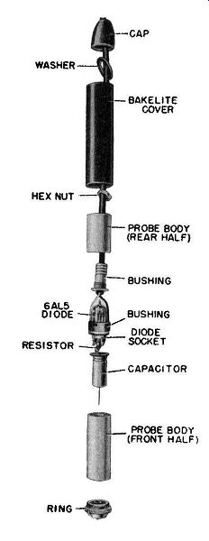
Fig. 6-4. Disassembled twin diode tube-type peak-indicating rectifier arranged
in probe form, for measurements for audio frequencies up to about 250 mhz.
The second diode section is used to balance out the contact potential of the
first one. Courtesy: RCA
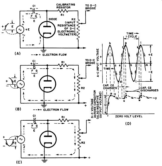
Fig. 6-5. (A), (B), (C) Basic circuit arrangement and action of a tube diode
rectifier for a vtvm, during one cycle of the a-c input voltage. (D) If an
a-c voltage (lower graph) is applied to the input circuit, a practically smooth
d-c voltage (upper graph) that is proportional to the peak value of the a-c
voltage, can be made to appear across the output circuit by proper choice of
the time constant of the R-C circuit network.
During the next half (b-c) of the positive alternation, the a-c input voltage decreases to zero, so that the voltage across the capacitor (due to its retained charge), now being greater than the input voltage, causes discharge current (electrons) to flow around the R-C network through the comparatively high resistance of R1 and R2 in series, as indicated in Fig. 6-2B. This partial, slow discharge of the capacitor causes its voltage to decrease, as indicated by the slope of s-t in part D of Fig. 6-2. Electron flow through the diode is cut off during this interval, because the sustained high negative charge on capacitor plate G makes the plate of the diode more negative than its cathode.
During the entire succeeding negative alternation c-d-e of the a-c input voltage, electron flow through the diode is still cut off, the capacitor continues to discharge slowly through the high-resistance R-C network as shown in Fig. 6-2C, and the voltage across it decreases along line t-u in part D of the same figure.
During the succeeding positive quarter-cycle e-f-g of the input voltage, the diode again begins to conduct when the input voltage reaches value f at which it equals the remaining capacitor voltage (the capacitor still has an appreciable proportion of its initial charge left). As the input voltage increases from f to its positive-peak value g, it charges the capacitor again, through the conductive diode, causing the voltage of the capacitor to increase from u to v, the latter being approximately equal to g, the positive-peak value of the a-c input voltage.
Thus, during this short interval the conditions are once again as illustrated in Fig. 6-5A. The foregoing actions repeat cyclically; while the a-c input voltage continues to go through its amplitude and polarity variations g-h-i-j-k-l-m, the d-c voltage which appears across the capacitor, and across R2, plus R1, varies in accordance with the graph v-w-x-y, etc.
It is evident that once the circuit assumes its steady operating conditions, the diode current (which is also the capacitor charging current) consists of a series of short bursts or pulses occurring on the successive positive peaks of the a-c input voltage. Each current pulse lasts for only a small fraction f-g, k-l, etc., of the total time required for the applied voltage to go through one cycle. While a tube diode is not conducting, its plate resistance is very high. It is this fact, combined with the fact that the shunting resistor network R1, R2 usually has a comparatively high resistance (of the order of 10 megohms and upwards in practical vtvm's), which makes possible the high input impedances which are achieved in practice with such tube-diode rectifier circuits. That part of the capacitor charge which leaks off through the resistance network R1, R2 is utilized for the voltage measurement since it causes voltage drops across the individual resistances. These voltage drops are directly proportional to the capacitor voltage and thus, the d-c voltage output of the rectifying circuit is directly proportional to the peak value of the applied a-c voltage.
It will be seen that resistors R1 and R2 in Fig. 6-5 act as a voltage divider, so they may be designed to apply any desired proportion of the total output voltage of the rectifier circuit to the input of the d-c voltage-measuring circuit of the instrument. This is very convenient whenever the rectifier is arranged in probe form (see Fig. 6-2C) to be connected to the D-C Volts terminal of a d-c vtvm. In this case, R1 and R2 may be so proportioned that only 0.707 of the peak value of the a-c input voltage actually appears across R2 and is applied to the d-c voltage input terminals of the d-c vtvm. The d-c voltage scales of the vtvm will then indicate directly the rms values (for sine waves only) of the a-c voltages presented to the rectifier probe for measurement. These scales may also be calibrated to indicate the peak values. R1 therefore functions as a convenient calibrating resistor.
In addition to the function already described, capacitor C1 serves also as a blocking capacitor to keep out of the instrument any d-c voltage component present in the circuit under test, so that only the a-c component of the voltage is measured. Consequently, this circuit may be used to advantage to measure peak values of a-c voltages that may be accompanied by a d-c component.
This is a peak-indicating rectifying circuit, and whether the vtvm indicates the positive-peak voltage or the negative-peak voltage depends on the polarity with which the diode tube is connected into the circuit. If connected as shown in Fig. 6-5 with its cathode tied to ground, the rectifier will respond to the positive-peak value of the a-c input voltage, since the diode will conduct only during the positive half-cycles of this voltage. If the rectifying circuit is in the form of a separate probe, the center lead of the shielded cable will then be negative with respect to ground, see Fig. 6-5B and C, so that the vtvm polarity must be set accordingly. No output is then produced by the probe if a series of negative pulses are applied to it. If the diode were to be connected into the circuit with its elements reversed to that shown here, the probe would respond to the negative peak value of the input voltage, and the center lead of the shielded cable would be positive with respect to the shield (Gnd). The half-wave shunt type of vtvm rectifier is also constructed in crystal diode form. This is discussed in Sec. 6-14.
6-4. Time Constant Requirements of VTVM Rectifying Circuits
Examination of Fig. 6-5D shows that the capacitor charges through the very low resistance of the diode tube only during the short portions f-g, k-l, etc., of the a-c input voltage cycles, and it discharges through the high resistance of R1 plus R2 during the much longer remainder of each cycle. It is evident that the conduction interval is very short as compared with the non-conduction interval.
For this reason, the mean diode current is very low, which means that the input resistance of the probe is very high. By limiting the conduction time of the diode to just a very small portion of each r-f cycle through the use of an R-C network which has a relatively long time constant, and by reducing the shunt input capacitance to a low value by suitable probe construction, a very high impedance may be presented to the source of signal. Therefore, very light loading of r-f circuits under measurement results. It is important to remember this.
[['For discharge of a capacitor through a resistor, the time constant, T, is defined as the time it takes the voltage across the capacitor to decrease by 63.2% from the initial value, i.e., the time it takes to discharge down to 36.8% of the voltage it had when it first started to discharge. In series R-C circuits, T = RC; T is in sec., where R is in meg, and C is in µ.f. Example: In the circuit in Fig. 6-SA, how long does it take for C1 to discharge to 36.8% of the original voltage across it, if C1 is 0.01 µ.f and R1 plus R2 is 40 meg.? T =RC= 40 x 0.01 = 0.4 sec. ]]
One charge and one discharge of the capacitor occurs during each cycle of the a-c input voltage. It is apparent that the time constant' of the R-C network must be designed to be sufficiently long so that the capacitor retains practically its full charge during the intervals s-u, v-w, etc. (Fig. 6-5), during which this discharge takes place. If this condition is realized in the design of the network, the voltage across the capacitor and that across network R1 plus R2, will remain substantially constant during these intervals instead of dropping as much as has been indicated in the exaggerated upper graph in Fig. 6-5D. A substantially smooth d-c voltage that is proportional to the peak value of the applied a-c input voltage will then appear across R2, and will be applied to the d-c bridge circuit of the d-c vtvm for measurement. This is the key to the proper functioning of a rectifier circuit for a vtvm. If the time constant is not sufficiently long, the rectified output of the probe gradually falls off in amplitude at the lower frequencies.
This attenuation at the lower frequencies results in a lowered voltage reading on the meter. Although the low-frequency attenuation can be decreased by using a larger value of capacitance for C1, this means an increase in the physical size of the capacitor and an increase in stray capacitance which may decrease the response at very high frequencies. Hence a practical compromise must be effected.
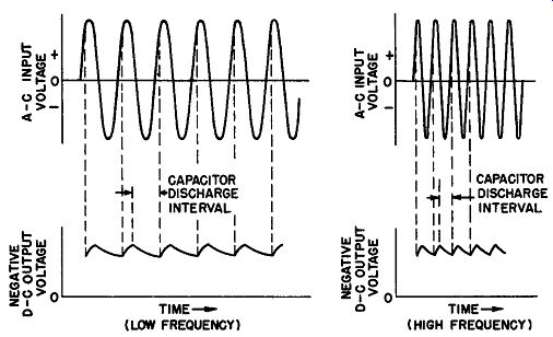
Fig. 6-6. Effect of the frequency of the voltage under measurement on the
time constant requirements of the rectifier circuit of a vtvm. A longer time
constant is required when a low-frequency voltage is to be measured, since
the time duration of the interval during which the R-C circuit capacitor is
required to discharge during each cycle is longer, the lower the frequency.
6-5. Effect of Input-Voltage Frequency Range on the Time Constant Requirements
Study of Fig. 6-5D shows that the value of capacitance C1 that is required to perform the smoothing function with practical completeness in a vtvm having a given input-resistance network, will depend on: (1) the frequency range of the a-c voltages that the vtvm will be called upon to measure; (2) the waveform of these voltages.
It is apparent that the higher the frequency of the a-c input voltage, the shorter is the duration of the discharge periods s-u, v-w, etc., of the capacitor, and therefore the less is the capacitance required to maintain a smooth d-c output voltage. This is illustrated by direct comparison in Fig. 6-6. Consequently, a value of capacitance that is sufficient for adequate smoothing at the lowest frequency to be measured, will be ample for all higher frequencies.
In general, for the measurement of sine-wave voltages, this capacitance should be made sufficiently large so that the time constant of the R-C circuit is approximately 100 times as long as the time required for the lowest frequency a-c input voltage to go through one cycle. To satisfy this condition, the capacitance of C should be not less than: 100 C = -- fR
where, C is in µF, f is in hz, and R is in megohms. If the capacitance is too small (time constant too short), the capacitor loses too much of its charge during each cycle, the average value of the voltage that appears across resistor R2 during each cycle will therefore decrease, and both the peak and the rms voltage indications of the vtvm will be lower than the true values of the applied voltage. For this reason, a proper combination of values of capacitance C1 and resistance R1 + R2 used in the rectifier circuit of a vtvm is chosen by the designer to achieve a discharge characteristic that provides accurate meter readings over the rated frequency range of the vtvm. For the measurement of pulse-type waveforms, a value of C larger than that specified in this frequency equation may be required, for the reasons explained in Sec. 6-10.
6-6. Waveform Error in RMS Voltage Measurements
In a peak-indicating type vtvm, the rectifying circuit response is on the basis of the peak value of the a-c input voltage. However, it is customary to design the resistance network R1, R2 so that only 0.707 of this voltage is applied to the d-c measuring circuit of the vtvm, so that the rms values of the ac may be indicated directly on the d-c voltage scales of the meter. This is done on the assumption that the waveform of the a-c voltage being measured is sinusoidal, in which case the 0.707 relationship holds true. However, if the waveform is not sinusoidal, that is if it contains appreciable harmonic voltage components, or other spurious voltages, the meter indication of the rms value may deviate from the true rms value by an amount that may be as large as the percentage of harmonic present, depending upon the phase relation between the fundamental and harmonic voltages. To illustrate the errors in measurement which may be caused by departure from sinusoidal waveform, the experimentally determined values in Table 6-1 (courtesy of Hewlett-Packard Co.) are presented.
For example, when a voltage of about 100 volts rms whose waveform contains 10 percent of third harmonic voltage is measured on such a peak-indicating type vtvm, the scale rms indication on the meter may be any value between 90 and 110 volts, depending upon the phase relation existing between the fundamental and the harmonic voltages.
Likewise, peak-to-peak type vtvm's are calibrated to indicate the p-p values of the a-c input voltage (regardless of the waveform). In addition, such vtvm's are usually provided with a scale calibrated in rms volts for a sine-wave input only. The readings obtained on this scale will be subject to the same error mentioned above if the waveform of the input voltage is appreciably distorted from true sine-wave form by the presence of harmonics.
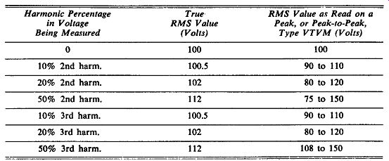
TABLE 6-1 ERROR IN RMS VOLTAGE MEASUREMENTS CAUSED BY HARMONICS
6-7. Contact Potential of the Tube Diode
One fact has been neglected in the discussion of the operation of the tube diode rectifier in Sec. 6-3. Even when no a-c voltage is being applied to the input terminals of the rectifier circuit, a minute current flows around the circuit comprising the diode tube and resistors R1 and R2 in Fig. 6-5A. This current is caused by the fact that some electrons leaving the heated cathode of the tube have initial velocities sufficient to carry them over to the nearby plate even when the plate is at zero potential, or even slightly negative, with respect to the cathode. Although this current is extremely small, it is usually enough to cause a small potential (typically 1-2 volts) to be developed across the resistors. This potential is negative with respect to the cathode. The result is that this small value of negative potential, called the contact-potential, is applied to the input grid of the d-c bridge circuit of the vtvm even when no a-c voltage is being applied for measurement. The contact potential is sufficient to slightly unbalance the bridge, and a small zero-volts deflection results. Therefore, a slight zero-adjustment of the meter would always have to be made when switching from d-c to a-c voltage measurement, or vice versa.
In order to permit the zero-volts adjustment of the meter to remain the same for both a-c and d-c voltage measurements, the contact potential of the tube diode must be neutralized by incorporation of a "bucking voltage" in the vtvm to cancel out the contact potential. Several methods of accomplishing this are employed. One method uses bucking voltage obtained from a dry cell and potentiometer combination. In another method, the contact potential of another diode is applied to the other grid of the bridge tube in order to balance the contact potential from the rectifier diode. Still another method taps the bleeder resistor in the power supply circuit to obtain the necessary small bucking potential.
6-8. Rectifying-Circuit Requirements for Peak-to-Peak VTVM The need for measuring the peak-to-peak voltage of both sinusoidal and complex non-sinusoidal waveforms and recurrent pulses found in tv circuits is discussed in Sec. 6-2. Several typical complex waveforms for which such measurements are frequently required are illustrated in Fig. 6-9. Although the oscilloscope is widely used for p-p voltage measurement of complex waveforms, it is sometimes desirable to also have a type of vtvm which will do this.
It might be supposed that the peak-to-peak value of any voltage waveform could be obtained by measuring the voltage with a peak-indicating type volt meter, reading the rms voltage value on its scale, and then multiplying this by the factor 2.83 to convert this rms reading to the peak-to-peak value. This is satisfactory only if the waveform under test is a sinewave, for only in this case is the rms value read on the peak-indicating type meter correct, and only in this case is the conversion factor 2.83 correct. This method is not correct for voltages having nonsinusoidal waveforms. Furthermore, nonsinusoidal waves usually have vertical dissymmetry (the positive-peak voltage is not equal to the negative-peak voltage), so that the conversion from rms to peak-to-peak voltage cannot be made at all for such waveforms unless the vtvm makes full provision for inherent measurement of the peak-to-peak voltage. Another type of rectifying circuit, the voltage-doubler, must be employed for this purpose.
It is sometimes thought, that a peak-indicating type vtvm can be employed to measure the peak-to-peak voltage value of a waveform by first measuring the positive peak value of the waveform with it, then measuring the negative peak value, by reversing its connections to the test circuit, and finally adding the two readings together to arrive at the peak-to-peak value. Commercial half-wave peak indicating service-type vtvm's cannot usually be thus "turned over" to measure the positive and negative portions of a waveform. Their rectifier circuits are such that they can indicate only the positive-peak value (or the negative-peak value, if the rectifier tube is wired up suitably), and one side of the a-c input circuit is generally grounded to the instrument case (see Fig. 6-2). Accordingly, if it is attempted to "turn over" a positive-peak instrument by reversing the connections to the circuit under test in order to measure the negative peak voltage, the ground terminal of the instrument is then applied to the "hot" side of the signal circuit under test, which capacitively shunts the signal circuit. This circuit loading frequently "kills" the signal voltage under test, with the result that a basic error in the reading results (the instrument reads low). It is evident that a type of vtvm rectifier circuit is required which will respond inherently on the basis of the peak-to-peak voltage of the signal under test, and so permit actual peak-to-peak voltage measurement to be made directly.
A voltage-doubler type rectifier having a suitably long time constant meets this requirement satisfactorily, since its d-c output voltage is equal approximately to the peak-to-peak value of the a-c input voltage, regardless of its waveform.
6-9. Tube-Diode Type Voltage-Doubler Rectifying Circuit for P-P Voltage Measurement
Voltage-multiplying rectifiers make it possible to obtain a higher direct voltage from a given a-c input than is possible with normal rectifier circuits. These circuits involve the principle of charging capacitors through rectifiers from the a-c input circuit, and adding their voltages in series for the d-c output; the switching is accomplished automatically by the rectifiers. Two capacitors and two diode rectifiers are used in a voltage-doubler rectifier. The diodes may be either the tube or the crystal type. When tubes are used, a twin-diode type is employed for convenience. Despite some operating advantages possessed by the full-wave type and by the conventional form of half-wave voltage doubler, the cascade type of half-wave voltage doubler is customarily employed, because the cascade circuit has the advantage of employing a common terminal between the input and the output circuits (see Fig. 6-7). Thus, both may be grounded simultaneously.
Built-in, and exterior-probe, arrangements of such rectifiers, and their connections to the d-c voltage divider and the amplifier-type d-c bridge circuit in the vtvm, are illustrated in Fig. 6-3A and B, and are described in the text relating to these illustrations.
The voltage-doubler rectifying circuit operates as follows: Referring to Fig. 6-7A, when the instantaneous value of the applied a-c voltage swings negative, an electron flow takes place as indicated, and C1 charges through diode V1 to the negative-peak value of the applied voltage. The polarity of the charge on C1 is as indicated. V2 is non-conducting during this interval, because its plate is negative with respect to its cathode.
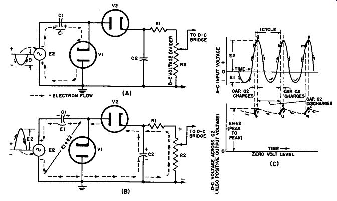
Fig. 6-7. (A), (B) Basic circuit arrangement and action of a cascade-type
tube diode half-wave voltage-doubler rectifier circuit during successive negative
and positive half-cycles of the a-c input voltage. (C) Graphs of the a-c voltage
input, and the d-c voltage output, showing the inherent peak-to-peak response
of this type of rectifier for any waveform.
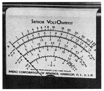
Fig. 6-8. Convenient direct reading d-c, rms (sine-wave), and peak-to-peak
(sine or complex wave) voltage scales available in a typical service type peak-to-peak
vtvm. Courtesy: RCA
On the succeeding positive half cycle of the a-c input voltage, diode V1 be comes non-conducting; therefore the charge on capacitor C1 cannot leak off through this path. Also, an inspection of Fig. 6-7B shows that the polarities are such that the a-c input voltage and the voltage of capacitor C1 are now in series with each other and therefore are additive. Accordingly, the negative-peak-value charge-voltage of C1, and the applied input voltage (up to its positive-peak value), added together are applied to the plate of V2. This tube now becomes conducting and permits a transfer of electrons to take place through the circuit, as shown in Fig. 6-7B, thus charging capacitor C2 to a voltage equal to the sum of the negative and positive peak voltages-which is the peak-to-peak value of the a-c input voltage (regardless of its waveform). As shown in Fig. 6-7B, C2 is able to slowly discharge continuously through resistances R2 and R1, and it actually continues to do so throughout the negative half-cycle action illustrated in Fig. 6-7A. This is shown more clearly in the graph in part C of the same figure. The resulting current flowing through R2 produces a voltage drop across it which is applied as the actuating potential to the d-c bridge amplifier in the vtvm.
Examination of Fig. 6-7C shows that once the circuit gets into operation, capacitor C2 charges only during the short peak portions f-g, k-l, m-n, etc., of the applied a-c voltage cycles, and it discharges through the load resistance, R1 + R2, during the much longer remainder of each cycle. Also, one short charge, and one long discharge, of the capacitor occurs for each cycle of the a-c input. By properly designing the R-C circuit C2, R1, R2 to have a time constant sufficiently long for the input-voltage frequency involved, the voltage across C2 may be maintained practically constant at the peak-to-peak value of the applied a-c voltage regardless of the waveform and what the proportions of the positive and negative peak are. Thus, the qualifications for an inherent peak-to-peak voltage measuring circuit are realized.
If the peak-to-peak voltmeter is to be arranged to indicate directly the rms values of sine waves, as well as the p-p values of both sine waves and complex waves, calibrating resistor R1 is usually included in the output of the doubler circuit. This is used to reduce the d-c output voltage of the doubler (across R2) to the rms value of a sine wave which has a p-p value equal to the p-p value of the complex wave. The d-c and rms (sine-wave) voltage scales of the vtvm are then identical, and another set of scales whose numerical values are 2.83 times those on the corresponding d-c and rms (sine-wave) scales are included to indicate the actual peak-to-peak value of the measured voltage (sine or complex wave). This convenient arrangement is possible only because the d-c voltage output of the voltage-doubler rectifier used here is proportional to the peak-to-peak value of the voltage wave under measurement. A set of scales for a typical vtvm of this type is illustrated in Fig. 6-8. Observe that both the rms and the p-p values of sine waves are indicated simultaneously (on adjacent scales) which is very convenient for some measurements.
The diode tube employed in the voltage-doubler rectifier is subject to the same contact potential effect that is discussed in Sec. 6-7, and this is usually counteracted by one of the methods discussed there. A voltage-doubler peak-to peak rectifying circuit has a lower input impedance than a peak-indicating type probe has, and its application may accordingly be limited to medium- and low impedance circuit testing. The voltage doubler also has a more limited frequency response. The maximum allowable input voltage is approximately the same as for a peak-indicating probe using the same type of rectifier.
Commercial variations of the voltage-doubler type of peak-to-peak rectifying circuit for vtvm's differ in form and in the range of signal voltages which may be accommodated. Both built-in, and exterior probe, arrangements (see Fig. 6-3) are in common use. This type of rectifying circuit, as explained in Sec. 6-17, has a counterpart in a similar circuit that employs germanium crystal diodes instead of tube diodes.
The peak-to-peak rectifying circuit can be provided with a switch to make available a choice of peak response or peak-to-peak response from one vtvm.
This arrangement is shown in Fig. 6-3C. Peak response is obtained when the switch is set to take the output from across the right-hand diode of the twin diode tube. Peak-to-peak response is obtained when the switch is set to utilize the entire twin-diode as a voltage-doubler rectifier. Details concerning the various indications obtained, etc., are the same as those explained in Sec. 6-18 for a crystal-diode version of this circuit.
The useful frequency range of most commercial service-type vtvm's which employ a twin-diode tube as a voltage-doubler rectifier extends to approximately 110 mhz. For measurement of a-c voltages above this frequency, a peak-indicating type rectifier arrangement using either a tube diode or a crystal diode (which have lower interelectrode capacitances than does the twin diode, see Table 6-2 in Sec. 6-ll), is usually employed. Details regarding such probes will be found in Sec. 6-3 and Sec. 6-14.
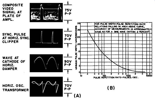
Fig. 6-9. (A) Typical narrow-pulse voltage waveforms of low repetition rate
en countered in tv receivers. Use of a p-p vtvm to measure the p-p voltages
of such waveforms may result in inaccurate readings. (B) Typical pulse-response
capability of a high-quality service-type vtvm. The graph shows the inherent
capability of the instrument. (B) Courtesy: RCA
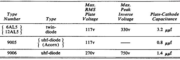
TABLE 6-2 OPERATING CHARACTER1STICS OF TUBE DIODES WIDELY USED IN VTVM's
6-10, Pulse-Response Capability of the Peak-to-Peak VTVM
Many of the non-sinusoidal voltage waveforms encountered in tv and other electronic equipment consist of narrow pulses having low repetition rates, as illustrated in Fig. 6-9A. If the peak-to-peak voltage values of such waveforms are measured with a peak-to-peak vtvm, it must be remembered that the capacitor in the voltage-doubler rectifier circuit may not be allowed sufficient time in which to charge fully during the extremely short-duration maximum-voltage period of the pulse, and the time interval between successive pulses may be too long for the partially charged capacitor to retain sufficient charge to maintain the d-c output voltage constant (see Fig. 6-7C). As a result, beyond certain limits of pulse width/pulse repetition rate, the peak-to-peak readings obtained will be lower than the true p-p value of the applied voltage. This is one of the reasons why a cathode-ray oscilloscope is widely used instead of a vtvm for measuring the p-p values of narrow-width low-repetition-rate pulse voltage encountered in tv service work.
The magnitude of this error caused in a typical high-grade service-type p-p vtvm is shown in Fig. 6-9B, which holds for essentially rectangular pulses obtained from a voltage source of 50 ohms impedance or less. For higher impedance sources, the error will be greater.
Since the rate at which the rectifier output capacitor discharges is deter mined by the input resistance of the d-c voltage-measuring circuit of the vtvm, it is apparent that the ability of a peak-to-peak vtvm a-c probe to measure the p-p value of very narrow pulses can be improved by increasing the time constant of the circuit. This may be done by adding series resistance in the output circuit of the probe to effectively double or triple the input resistance of the vtvm.
Then the discharge current is small enough to permit the charging capacitor to maintain practically its full charge from the peak of one pulse to the peak of the next one. However, in such cases, the a-c scale range of the instrument is also doubled or tripled, by this "multiplier" resistance so that low voltages can no longer be read accurately. An alternative is to use the rectifying probe with a vtvm having a higher input resistance if the voltages of narrow pulses are to be measured.
6-11. Important Operating Characteristics of the Tube Diode (1) Curvature of Lower End of Diode Characteristic. The typical plate voltage plate-current characteristic of a tube diode is shown in Fig. 6-10. It will be seen that the characteristic is linear over most of the plate-voltage range.
However, beyond a certain value of plate voltage, additional plate voltage has little effect in increasing the plate current. This is the saturation voltage area of the tube operation. Also, note that a small current flows when the plate voltage is zero, or even slightly negative, leading to the contact potential effects discussed in Sec. 6-7. Furthermore, the lower end of the characteristic is curved, causing the current to become less in proportion to the plate voltage, at low plate voltages. Consequently, when a diode tube is used as the rectifier for a vtvm, the low-volts portion of the a-c voltage scale is non-linear-usually in the region below approximately 3 volts. The same operating characteristic, non linearity at low input voltage, also occurs for crystal diodes.
(2) Electron Transit Time and Diode Behavior at UHF. In diode-rectifier applications at comparatively moderate frequencies, the transit time of the electrons (time required to travel from the cathode to the plate) is short compared with the period (time required for one cycle) of the applied a-c voltage. As the frequency is increased, this becomes less and less true until finally, frequencies are reached for which an appreciable fraction of a cycle is required for an electron to pass from the cathode to the plate. When this happens, the behavior of the tube changes markedly. The dynamic plate resistance of the diode drops (at certain frequencies it may even become negative), and there are also modifications produced in the effective plate-cathode interelectrode capacitance. Several uhF type miniature diodes designed especially for satisfactory operation at uhF are widely used in the rectifying circuit of peak, and peak-to-peak type vtvm's.
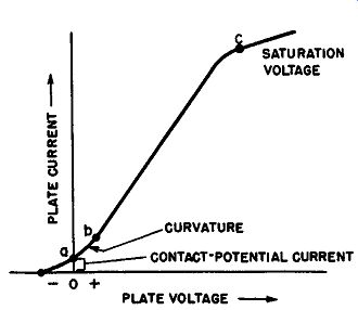
Fig. 6-10. Contact potential and curvature of the lower end of the operating
characteristic are shown here for a typical tube diode.
(3) Input Resistance and Capacitance. The diode tubes employed in vtvm's must have high input resistance (when not conducting) and low plate-cathode capacitance so that the input impedance of the rectifier circuit will be sufficiently high to prevent excessive loading of the circuit whose voltage is to be measured.
The modern miniature uhF diodes commonly used are satisfactory in this respect (see Table 6-2 for typical values). It must be remembered that when the diode rectifier is built into the vtvm case, necessitating the use of a shielded direct cable to the test point, the comparatively large input capacitance of the shielded test cable is added to that of the diode and is applied across the circuit under going test.
(4) Peak Voltage Rating. The diode tube will be damaged by the application of excessive input voltage, but it is much less susceptible to permanent dam age from this cause than is the crystal type diode. The maximum rms plate voltage ratings for several diode tubes that are widely used in vtvm's are tabulated in Table 6-2. If voltages in excess of these ratings are to be measured, an a-c voltage-divider must be employed ahead of the rectifier, as in Fig. 6-2A and Fig. 6-1A, and then both the divider and the rectifier must be located within the instrument case. This must be a frequency-compensated type divider if good high-frequency response is to be maintained. It can be seen that the maximum voltage ratings of tube diodes are very much higher than the approximately 28 volt (peak) rating of the germanium crystal diodes most widely used in rectifying probes.
(5) General. The important characteristics of several types of tube diodes that are widely used in the rectifying circuit of service-type peak and p-p vtvm's are tabulated here: 6-12. The Crystal Diode and its Operating Characteristics The germanium crystal diode is a compact, light weight, heaterless diode that is widely used for low-power rectification at frequencies up to approximately 250 mhz. It has a low shunt capacitance of approximately 1 µ.µ.f, and is extremely efficient in applications where low-voltage a-c signals must be rectified. The general-purpose 1N34 (and 1Nll4A) type is widely used as the rectifier in the high-frequency rectifying probes for vtvm's (see Fig. 6-11, and Fig. 6-2B). The circuitry and mode of operation of the rectifier circuits are basically the same when the crystal diode is employed as when the tube diode is used. However, there are some minor differences, and these will be pointed out. One of the advantages of the use of a crystal diode instead of a tube diode in a rectifying circuit constructed in probe form, is that the former is very small in size and does not require any heater circuit wiring to be brought up to the probe through the connecting cable. Its excellent high-frequency characteristics also, make it useful for high-frequency voltage measurement, or indications up to approximately 250 mhz.
When an alternating voltage is applied to a germanium diode, it tends to cause electrons to flow through the diode, in opposite directions, during each half cycle. The diode presents a certain resistance to the flow of electrons in the direction from the germanium wafer (cathode) to the cat whisker (anode), but it presents a much higher resistance (approximately 1,000 times as much) to the flow of electrons in the opposite direction. This action is repeated for each cycle.
Consequently, almost complete rectification takes place. The direction of electron flow for which the crystal diode is most conductive (least resistance offered) is called the forward direction; the applied-voltage polarity which produces electron flow in this direction is called the forward voltage; the current which is then flowing is called the forward current; the resistance to electron flow in this direction is called the forward resistance. The opposite electron-flow direction, voltage-polarity, current, and resistance are called, respectively, the reverse direction, inverse voltage, reverse current, and reverse resistance. The term back is sometimes used instead of reverse.
A comparison of the crystal versus the tube diode reveals that they are basically similar in their effect on the current flow in the circuit, except that because the crystal diode offers a finite value of resistance to the flow of electrons (current) in the reverse direction, it allows a small reverse current to flow, whereas the tube diode does not (compare Fig. 6-12 with Fig. 6-10). The voltage-current characteristic of a 1N34 general-purpose type germanium crystal diode is shown in Fig. 6-12. (Important notes concerning the scales employed on this illustration will be found in the caption). It will be seen that there is no current flow at zero applied potential; therefore the crystal diode is free from contact potential effects, and no bucking-voltage source is required.
This is an advantage over the tube diode.
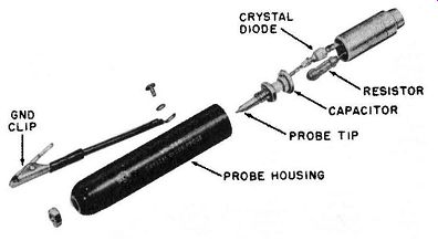
Fig. 6-11. High-frequency crystal-diode rectifying probe for vtvm disassembled
to show the construction and various component parts. Courtesy: RCA
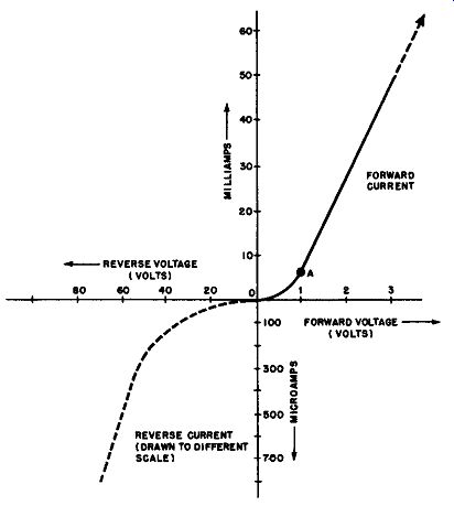
Fig. 6-12. Average voltage current characteristic (static) of the 1N34 and
1N34A crystal diode which is widely used in high-frequency rectifying and demodulating
probes. Observe that there is no contact potential current for the tube diode;
also that some reverse current flows when the applied voltage is reversed.
The conduction in the forward direction is over 1,000 times greater than that
in the reverse direction. Note that in the graph above, the forward conduction
is plotted in milliamperes, while it was necessary to plot the small reverse
conduction in microamperes (only 1/1000 as much) in order to show the reverse-current
magnitude at all. Also, the voltage scales are unequal. Courtesy: Sylvania
Elect. Prod. Inc.
The characteristic is curved quite appreciably for low input voltages up to approximately l volt (point A), so the output is less in proportion to the input voltage at low signal levels, as in the case of the tube diode. In fact, for input voltages up to approximately 0.2 volt, the output is usually proportional to the square of the input voltage. For this reason, a crystal diode is a typical square-law rectifier for very small input voltages of this order. Above the 1-volt region, the output becomes practically proportional to the input voltage, as evidenced by the straight-line characteristic, so the crystal diode is regarded as a linear device at input voltages over this range. It is important to remember this in the application of crystal-diode type rectifying or demodulating probes.
The 1N34 germanium crystal diode, which is the type most widely used in crystal probes, has a nominal shunt capacitance of approximately 1 µµF. This is somewhat lower than that of the widely used tube type 6AL5 or 12AL5 twin diodes, but slightly greater than that of the 9005 uhF tube diode (acorn type), see Table 6-2.
The electrical specifications of the 1N34 crystal diode are as follows:
Maximum continuous reverse working voltage _ 60 v
Maximum reverse current at -10v, ___ 50 µa
Maximum reverse current at -50v 500 µa
Forward current at +1v __ ...:., ma
Average anode current 0 ma max.
Recurrent peak anode current 150 ma max.
Instantaneous surge current. _ ...,oo ma max. 1 sec.
Germanium crystal diodes permit the construction of rectifying probes which have low input capacitance, but they will not withstand as much input voltage as does a tube diode. The maximum a-c voltage which should be applied to the input of a conventional rectifier probe that employs a IN34 germanium crystal diode is approximately 20 volts rms, or 28 volts peak. If a d-c component is present, it should not exceed the voltage rating of the series capacitor in the rectifier circuit. On the other hand, a tube diode used in such an application can be used with input voltages in excess of 100 volts (see Table 6-2). When necessary, a number of crystal diodes may be connected in series to raise the maximum voltage capability of the rectifier.
The IN34 germanium diode characteristic illustrated in Fig. 6-12 is an average characteristic. The characteristic of a specific crystal diode unit depends on the particular germanium crystal used, the contact, the contact pressure, etc.
Consequently, the characteristics from unit to unit, especially the forward resistance and the back resistance, will be found to show comparatively large variations. Variations in crystal forward resistance affect the calibration of the associated meter directly if a simple series rectifying circuit is used, but if a peak indicating rectifying circuit is employed, only the small difference between the peak applied voltage and the developed d-c voltage depends upon the crystal characteristics.
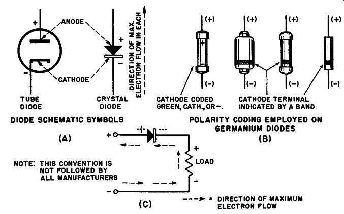
Fig. 6-13. (A) Standard crystal-diode and tube-diode symbols arranged side
by side for comparison. The direction of maximum electron flow is from the
cathode to the anode, inside the diode, in both types. The arrow in the crystal
diode symbol thus points opposite to the direction of the maximum electron
flow within the diode. (B) The polarity coding employed on various models of
germanium diodes. The cathode terminal is always indicated by either a minus
sign or a colored band. The polarity coding on germanium diodes indicates the
voltage polarity that must be applied to obtain maximum current flow. (This
should not be confused with the polarity coding of selenium rectifiers, which
is the output polarity developed across a load.)
------------
TABLE 6-3 COMPAR1SON OF IMPORTANT PROBE-PERFORMANCE FACTORS OF CRYSTAL DIODES & TUBE DIODES
Performance Factor Crystal Diodes Tube Diodes
Contact potential None Enough to require a bucking-voltage circuit
Input resistance Low High ( forward direction) ( order of a few (ranges from 15,000 hundred ohms) to 120,000 ohms)
Back resistance
Relatively low
Very high ( 100,000-to ( open circuit) 200,000-ohms range)
Tolerance on characteristics Fairly wide variation Greater uniformity from one unit to another Max. permissible 20 v rms for 1N34 Approx. 117 to 300 v input voltage Susceptibility to Quickly damaged Less easily damaged voltage-overload damage High-frequency Good Poorer, due to response transit time Small-signal Good Poorer, due to less Efficiency curvature of characteristic Ability to make Good Poor, due to variation relative-value readings of transit time with above resonant signal level frequency of probe Temperature Relatively Good stability poor
---------------------
The standard schematic symbol employed for a crystal diode is shown in Fig. 6-l3A, alongside of that for a tube diode, for comparison. It can be seen that the direction of maximum internal electron flow is from the cathode to the anode in each case. The standard polarity coding employed on germanium diodes is illustrated in Fig. 6-13B. Important details concerning both are explained in the caption. The polarity of the d-c voltage developed across a load connected in series with a crystal diode is shown in Fig. 6-13C. The pertinent performance factors of the types of crystal diodes and tube diodes that are commonly employed in rectifying and demodulating probes are presented here in Table 6-3 for direct comparison and study.
6-13. Series-Type Peak-Indicating Crystal-Diode Rectifying Probe The series type of rectifying circuit utilizes the diode rectifier in series with the input circuit.
(1) Single-Ended Type. Two versions of this type of circuit arranged as a probe for use with a vtvm are shown in Fig. 6-14. In the simplified version in part A of the figure, the crystal diode feeds directly into the shielded test cable whose internal capacitance C serves as the charging capacitor. This simplified construction avoids the loss due to voltage drop in the isolating resistor R1 in Fig. 6-14B, but it is not useful at frequencies above which the cable operates as a tuned stub (usually above the i-f frequency range), because the pulsating rectified output voltage undergoes sharp increases and decreases at some frequencies due to resonance effects which occur in the cable. Also, the value of C is not easily controlled.
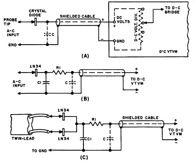
Fig. 6-14. Three versions of the series type crystal-diode peak-indicating
rectifying circuit arranged in a probe for use with a vtvm. The double-ended
circuit in (C) is useful for checking voltage in a 2-wire transmission line.
The rectified current which flows through the crystal diode on alternate half cycles charges capacitance C to almost the peak value of the a-c input voltage. The capacitor discharges through the d-c voltage-divider resistance of the vtvm, and also through the path presented by the back resistance of the crystal diode, during the remainder of the cycle. The resulting d-c voltage developed across the d-c voltage divider of the vtvm is applied to the d-c bridge tube in the vtvm for measurement. Obviously, the time constant of the R-C circuit must be made long enough to produce a smooth d-c output voltage for a-c input voltage of any frequency within the rated frequency range of the instrument.
This is a peak-indicating rectifying circuit, and whether the vtvm will indicate the positive-peak, or the negative-peak, value of the a-c input voltage depends upon which way the crystal diode is connected into the circuit. If it is connected with the polarity as indicated by the crystal-diode symbol in Fig. 6-14A, the probe will respond to the positive-peak value of the input voltage, for the diode will be conducting only during the half cycles when the probe tip is positive with respect to the Gnd terminal. The center lead of the shielded cable will be positive under this condition, so that the vtvm must be set accordingly. No output is produced by this probe if a series of negative pulses are applied. If the diode were to be connected into the circuit with its polarity the reverse of that shown here, the probe would respond to the negative-peak value of the input voltage, and the center lead of the shielded cable would be negative.
An improved, preferred arrangement of the series-rectifying circuit in which a charging capacitor, C1, and an isolating resistor, R1, are used is shown in Fig. 6-14B. This is useful to higher frequencies, because isolating resistor R1, C, and C1, form a low-pass filter which helps to prevent voltage pulses from entering the shielded cable, hence cable resonance effects are minimized. (Resistor R1 may be made to serve also as a calibrating resistor for the vtvm.) Neither arrangement is suitable for uses in which a d-c component is present along with the a-c voltage, because this will cause the crystal diode to be dam aged or to bias off, thereby causing the a-c operating-voltage swing to occur over a region of the characteristic curve that may produce very incomplete rectification or, even none at all.
The series rectifier arrangement has the advantage of providing minimum input capacitance to the probe.
(2) Double-Ended Series-Type Peak-Indicating Rectifying Circuit. The series-type crystal-diode rectifying circuit is often used by the technician in the form illustrated in Fig. 6-14C. The double-ended probe is used to measure voltages on 2-wire transmission lines, for example, and is useful because it applies a minimum of input capacitance across the line under test, and causes the least disturbance of line impedance. It is quite possible to use a shunt type of rectifying arrangement to measure transmission line voltages, but the stray capacitance and input capacitance are greater, and since d-c voltages are seldom present in the line, the series arrangement is practical and to be preferred. The two crystal diodes do not conduct simultaneously. Insofar as the instantaneous voltages which appear across the line are concerned, when the input voltage to one diode is positive, that to the other diode is negative. These polarities alternate at the carrier frequency; hence the diodes conduct alternately. Charging capacitor C1 is charged alternately through the two diodes. Resistor R1 effectually isolates the shielded cable from the high-frequency portion of the circuit.
6-14. Shunt-Type Peak-Indicating Crystal-Diode Rectifying Circuit
The shunt type of peak-indicating rectifying circuit in which a crystal diode is employed is widely used in probe form as a high-frequency rectifier for vtvm's.
When so employed, it is frequently referred to by the somewhat vague term "r-f probe." The circuit is shown in Fig. 6-15, and it will be apparent at once that the circuit arrangement and operation are basically similar to that of the shunt type tube-diode rectifying circuit described in detail in Sec. 6-3, and illustrated in Fig. 6-5. The voltage which appears across the terminals of input capacitor C1, as a result of the charge developed in it, constitutes a bias on the crystal diode. This shifts the operating point of the crystal to a more negative (lower current) region of its characteristic curve. The charge on the input capacitor…
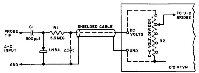
Fig. 6-15. Shunt-type crystal-diode peak-indicating rectifying circuit widely
used in probe form for measuring sine-wave radio-frequency voltages with a
d-c vtvm.
Rectifying circuits of this type, constructed in probe form, can usually be used up to 100 to 250 mhz with an accuracy of ±10%. Observe the simplicity of this arrangement-no heater-supply wiring, or contact-potential bucking-voltage circuit is required as it is when a tube type diode rectifier is employed.
... escapes slowly through the parallel circuit composed of the back resistance of the crystal and R1 plus R2 in series. The operating level comes to equilibrium at a point where the small charging current pulses exactly equal the total leak age losses. For this reason, the input capacitor charges up to a voltage almost, but not quite equal to, the peak voltage of the applied signal.
Referring to Fig. 6-15, it will be observed that series resistor R1 serves the important function of r-f isolation, as well as its usual calibrating function.
It is plain that if R1 were omitted, the cable capacitance, C, would shunt and tend to short-circuit the crystal at high radio frequencies.
Radio-frequency input voltages as high as 20 volts rms, or 28 volts peak, may be applied directly to the input of such a rectifying circuit when a 1N34 crystal diode is used. If a d-c component is present in the a-c voltage to be measured, it should not exceed the safe voltage rating of capacitor C1, which serves the dual role of charging capacitor and d-c blocking capacitor. The upper operating frequency range is approximately 250 mhz, but the exact value depends greatly on the mechanical and electrical design of the probe.
This type of rectifying probe is customarily used to measure high-frequency sine-wave voltages when it is plugged into the D-C Volts terminals of a vtvm.
It is customary to specify sine-wave voltages in rms values (0.707 of peak value). Accordingly, if the vtvm is to indicate the rms values, and these are to be read directly on the existing d-c voltage scales of the vtvm, the value of calibrating resistor R1 must be selected so that only 0.707 of the full d-c output voltage of the rectifier circuit will be applied across the d-c voltage divider R2 inside the vtvm. If the d-c voltage-measuring network of the vtvm is designed on the basis of using the usual circuit-isolation resistor in the "d-c probe" supplied with the vtvm (see Section 4), the value of this isolation resistor, which we shall call R3, must be added to the calculated value for R1, for the a-c probe will be feeding directly into the vtvm without this isolating resistor. For rms readings on the d-c voltage scales then, R1 must equal 0.414 X (R3+R2)+R3. (Note: The ratio…
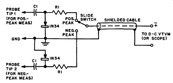
Fig. 6-16. A special peak-indicating probe arranged to provide either positive
peak or negative-peak indication, as desired. This general circuit arrangement,
employing suitable values for C1 and Rt, may also be employed with a scope.
…between 1-.707 and .707 is 0.414.) For a 10-megohm input instrument that normally employs a I-megohm isolating resistor in the d-c probe, R1=0.414X (1+10)+1=5.554 megohms. In practice, a slightly lower value would he used, as shown in the figure, to compensate for the fact that slightly less than peak rectification occurs.
Because of the inherent non-linearity of the crystal-diode operating characteristic at low input voltages, a special calibration is required for a-c scales on which voltages below about 1 volt are to be lead.
The meter scale rms readings can be multiplied by 1.414 in order to convert to peak voltage (to which the probe actually responds). The lowest frequency that can he handled satisfactorily by the rectifying circuit will depend on the time constant of the R-C circuit. In general, for the measurement of sine-wave voltages, the capacitance of C1 should be not less than C1 = 100//U in order that a sufficiently long time constant be provided for adequate filtering of 'the output voltage (see Sec. 6-4 and Sec. 6-5). The calculation for C1 should not neglect the effect of the back resistance of the crystal diode in allowing some of the charge of capacitor C1 to leak through it during the non-conducting half cycles. This back resistance, being in parallel with R1 and R2, tends to shorten the time constant somewhat. With the 500-itµf capacitor employed, as shown in Fig. 6-15, the lowest usable frequency is in the order of 50 khz. The breakdown-voltage rating of C1 determines the amount of d-c voltage that may be present along with the r-f signal that is to be measured. A typical value is 250 volts.
The highest frequency which can be handled is limited by several important factors related to the probe and test cable design. These are discussed in Sec. 6-21.
This probe employs a peak-indicating rectifying circuit, and whether the vtvm indicates the positive-peak or the negative-peak voltage depends on the polarity with which the crystal diode is connected into the circuit. If it is connected as in Fig. 6-15, with its cathode connected to ground, the probe will respond to the positive-peak value of the a-c input voltage, since the crystal diode will then conduct only during the positive half-cycles of this voltage. The center lead of the shielded cable will then be negative with respect to ground; so that the vtvm must be set accordingly. No output will be produced by the probe if a series of negative pulses are applied. If the diode were to be connected into the circuit with its polarity the reverse of that shown here, the probe would respond to the negative-peak value of the input voltage, and the center lead of the shielded cable would be positive.
6-15. Combination Positive-Peak or Negative-Peak Probe
The foregoing principles may be applied in a special form of peak-indicating probe designed to provide, conveniently, either positive-peak or negative peak indication. This feature is frequently quite useful in testing the output of a signal generator. For example, one where the waveform may not be a true sine wave, and the positive and negative peaks are unequal. A switching arrangement is employed to reverse the polarity of the crystal diode for either type of indication.
Because it is impractical to switch the crystal diode (due to introduction of excessive stray capacitance in the high-frequency circuit), the polarity switching is accomplished in the output d-c network, and two crystal diodes are employed as shown in Fig. 6-16. Each of the diodes is connected to an individual probe tip, so that the input capacitance to either of the diodes is no greater than in the case of a simple single-diode probe.
For use with a vtvm, C1 and R1 may have values of approximately (1.01 µI and 5 meg, respectively. for scope use, values of approximately 0.00025 µf and 200,000 ohms may be employed in order to provide a more suitable time constant.
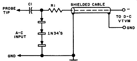
Fig. 6-17. High-impedance peak-indicating crystal probe which employs a number
of crystal diode rectifiers in series.
6-16. High-Impedance Type Peak-Indicating Crystal-Diode Rectifying Circuit
When a crystal-diode probe is used with a vtvm, the pr!)be may excessively load down a high-impedance circuit under test and disturb its operation. In such a case, the technician needs a probe having a higher input impedance.
The input impedance may be increased by employing two or more crystal diodes in series, as shown in Fig. 6-17. The impedance of this type of crystal ...

Fig. 6-18. A basic peak-to-peak indicating probe employing two crystal diodes
in a voltage-doubler rectifying circuit. This arrangement is very useful in
tv troubleshooting to measure the peak-to-peak voltage values of complex wave
forms in order to compare them with the specified values.
... probe is higher than usual because the rectifier resistance is increased by a factor equal to the number of rectifiers employed, and also because the input capacitance is decreased by the series arrangement of the rectifiers. The fact that the maximum allowable input voltage is also increased in proportion to the number of rectifiers used may be advantageous in some applications.
Several precautions must be observed in the construction of a probe of this type in order to minimize the input capacitance so that the input impedance will be high. First, a button-type capacitor should be used for C1; second, the crystal diodes, C1, and isolating resistor, R1, should be kept well spaced from the shield of the probe; third, a short probe tip should be used, and it should not be terminated with a test clip.
6-17. Peak-to-Peak Crystal-Diode Rectifying Probe
A peak-to-peak rectifying probe which employs two crystal-diode rectifiers in a basic cascade type voltage-doubler rectifying circuit, is shown in Fig. 6-18.
The circuit action is similar to that described in Sec. 6-8 and Sec. 6-9, and illustrated in Fig. 6-7 for the tube-diode voltage-doubler rectifier. As before, a calibrating resistor R1 is included, and this also serves the function of minimizing disturbances clue to cable resonances within the rated frequency range of the probe.
The calibrating resistor value is chosen so that when operating in conjunction with the input resistance of the vtvm, the rms value of a sine-wave voltage is indicated directly on the d-c voltage scales of the vtvm (see Sec. 6-9). A voltage-doubler peak-to-peak probe has a considerably lower input impedance than a peak-indicating type probe, and its application may accordingly be limited to medium and low-impedance circuit testing. The voltage-doubler probe also has a more limited frequency response. The maximum allowable input voltage is approximately the same as for a peak-indicating probe using the same type of rectifier. The various considerations concerning pulse-response capability, which are discussed in Sec. 6-10, apply to the crystal-diode type of peak-to peak probe as well as the tube-diode type.
Before undertaking to make peak-to-peak voltage measurements using a crystal-diode type voltage-doubler probe in combination with a particular vtvm, the operator should check the scale indication of his vtvm against a known source of peak-to-peak voltage in order to determine the attenuation factor of the probe. Since the input resistance of various vtvm's is different, and since the front-to-back resistance ratio of individual crystal diodes is different, the voltage doubler probes should be individually calibrated for insertion loss.
6-18. Combination Peak and Peak-to-Peak, Crystal-Diode Rectifying Probe
The peak-to-peak crystal-diode rectifying circuit can be provided with a switch to make available a choice of positive-peak or negative-peak, and peak-to peak voltage measurements, by means of an arrangement such as that shown in Fig. 6-19. The switching takes place on the d-c side of the rectifying circuit and thus does not impair the frequency response of the probe.
When the circuit-selector switch is set at the P position, the rectifier circuit will respond on the basis of the positive-peak voltage. If calibrating resistor R1 has the proper resistance value, so that 0.707 of this peak voltage is applied to the vtvm, the vtvm will indicate the rms values directly on the d-c voltage scale (for sine waves only). However, even if the input voltage waveform is non sinusoidal, the scale indication is still meaningful if multiplied by 1.414 to yield the positive-peak voltage of the applied signal.
When the switch is set at the P-P position, the circuit operates as a voltage doubler rectifier and the rectifier circuit responds on the basis of the peak-to-peak value of the input voltage, regardless of its waveform. Resistor R3 is made equal to the value of the isolating resistor employed in the "d-c probe" of the d-c vtvm. The vtvm then indicates peak-to-peak values directly on the d-c voltage scale. The negative-peak voltage may be obtained by first calculating the positive peak value as explained above, and then subtracting this from the measured peak-to-peak voltage.
6-19. VOM R-F Peak-Indicating Rectifying Probe
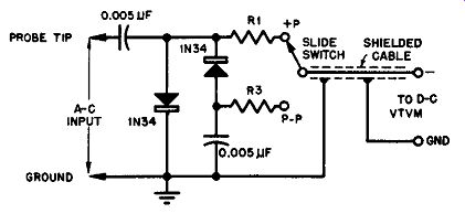
Fig. 6-19. Crystal-diode probe switching arrangement for obtaining either
the peak value, or the peak-to-peak value, of a complex waveform. By pro viding
a vtvm with such a probe, some of the facility afforded by a scope is realized.
Although the probe-plus-vtvm combination does not give in formation concerning details of the waveshape, it can be used to reveal any dissymmetry which may be present, by developing information concerning the positive-peak voltage, the peak-to-peak voltage, and hence also, the negative peak voltage of the waveform.
The a-c voltage-measuring function of a typical service-type non-electronic vom usually employs a built-in copper-oxide rectifier. The frequency response of such a combination decreases gradually as the frequency increases. In a typical case, the readings obtained on a 20,000 ohm-per-volt vom decreased to 70 percent of the correct value at a frequency of 60 to 90 khz (depending on the voltage amplitude being measured). However, a conventional simple crystal-diode peak-indicating type rectifying circuit, built in the form of an external probe, can be used in place of the copper-oxide rectifier. In this case, the vom becomes a very handy instrument for indicating the presence, or comparative values, of r-f voltages of almost any waveform. Such voltage indication is useful in some signal tracing and other work when it is necessary only to determine the presence, absence, or relative magnitudes of a signal across certain test points of medium or low impedance in the equipment under test.
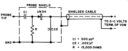
Fig. 6-20. R-F probe which makes possible the use of a service-type vom for
indicating the presence, or comparative values, of r-f voltages of almost
any waveform.
A peak-indicating rectifier suitable for this purpose when used with a vom of at least 5,000 ohms-per-volt sensitivity, is illustrated in Fig. 6-20. Its output is connected to the D-C Volts terminals of the vom.
The input resistance of this combination is necessarily quite low because of the comparatively large current drain imposed by the low-voltage ranges of the vom that would be used (as compared with the current drain of a d-c vtvm). As a result, it appreciably loads any high-impedance voltage source to which it is applied. Consequently, the actual voltage readings obtained when checking such circuits, are likely to be so far below the potentials actually present before the combination is applied that any attempt at actual r-f voltage calibration of the meter for use in such circuits is useless. Consequently, use of the combination must be limited to r-f voltage-presence and relative-strength indications only, for such circuits. However, if the meter is suitably calibrated, measurement of r-f voltage in low-impedance circuits, such as signal-generator output cables, etc., can be accomplished satisfactorily.
6-20. Typical Shop-Constructed VTVM R-F Rectifying Probes
Peak, and peak-to-peak rectifying probes for use with d-c vtvm's are avail able in manufactured form, or they may be assembled by the service technician to meet his own requirements. The schematic circuit diagrams of a number of very useful shop-constructed vtvm probes recommended by tv receiver manufacturers are shown in Fig. 6-21. They are designed to have the various operating characteristics specified, and perform useful functions in tv receiver service work.
If these probes are employed for voltage-presence or relative-strength indications only, no calibrating resistor need be used with them. However, if actual voltage measurements are to be made, a calibrating resistor whose value depends on the input resistance of the vtvm with which the probe is to be used will be required. The method of calculating the value required for peak, and for peak to-peak, indicating circuits is explained in the sections of this section devoted to these types of circuits. Probe construction details are discussed in Sec. 6-22, and measurement accuracy considerations are explained in Sec. 6-23.
------------------------------
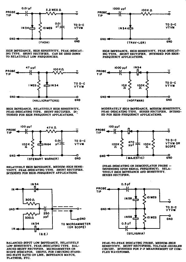
Fig. 6-21. A number of useful shop-constructed r-f rectifying probes for
use with d-c vtvm's in tv receiver servicing, as suggested by the various tv
receiver manufacturers noted.
------------------
TABLE 6-4 EFFECT OF RECTIFIER ARRANGEMENT ON INPUT RESISTANCE & CAPACITANCE OF VTVM's
-------------------
6-21. High-Frequency and Low-Frequency Operating Characteristics of VTVM Rectifying Probes
The a-c voltmeter function of many modern vtvm's that employ a built-in rectifying circuit is suitable for accurate voltage measurement over a frequency range whose upper value is only 15,000 cycles in one service-type instrument, and approximately 3 mhz in several other models. One of the chief reasons for this limited frequency range is that the r-f energy to be measured must pass through the shielded test cable before it reaches the rectifying circuit. The shunting effect of the comparatively large distributed capacitance (ranging between approximately 50 and 200 uf) of the cable causes appreciable attenuation of the input voltage as the frequency of the voltage undergoing measurement increases.
Quite aside from this is the appreciable error introduced by the severe circuit loading and detuning effects which the comparatively low input-impedance of such a test cable causes if it is applied to most types of high-impedance r-f circuits (see Section 3). These difficulties are partially overcome by the exterior-probe arrangement where the rectifying circuit is brought as dose to the point of measurement as is feasible thus eliminating the long connection circuit between the r-f voltage source and the rectifier. This reduces the input capacitance to a very much lower value, and at the same time reduces resonance effects in the test cable since the test cable now serves to conduct mainly filtered rectified current instead of the r-f energy. The data in Table 6-4 is compiled from the manufacturers' specifications for several representative service-type vtvm's which employ a built-in rectifying circuit for a-c voltage measurements over the lower-frequency range of the instrument, and use an exterior rectifying probe for voltage measurements over the higher-frequency range to several hundred megacycles. It serves to illustrate the marked reduction in input capacitance (with resulting increase in input impedance) that is achieved mainly by arranging the rectifying circuit in an exterior probe. Thus, the r-f rectifying probe not only presents a means of measuring higher-frequency r-f voltages more accurately, but with proper design its input impedance may be kept high so that it presents a comparatively light load to the a-c circuit under test. The amount of error due to circuit loading is dependent, of course, on the impedance of the source of the a-c voltage being measured.
(1) High-frequency Response Characteristics. At high frequencies, the rectifying probe circuit becomes complex due mainly to stray capacitances. As a result of the complex circuit, the effective input capacitance and impedance fall to relatively low values at very high frequencies, and if the frequency is increased sufficiently, the output voltage from the probe eventually drops to zero. This is illustrated in Fig. 6-22. At frequencies where both vary with the frequency, the probe presents a complex, low-impedance, non-linear circuit to the source of voltage under test.
Some rectifying probes are subject to important residual resonances (especially above 100 or 200 me) before the input impedance drops to an excessively low value. This resonance will cause excessive peaks and valleys in the high frequency characteristic of the probe, with the result that the voltage indication on the vtvm becomes higher or lower than the actual value of the voltage under test.
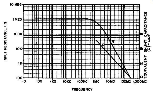
Fig. 6-22. Variation of the effective input resistance and capacitance, with
frequency, for a peak-to-peak rectifying probe employing a 6AL5 twin-diode
rectifier. Courtesy: RCA
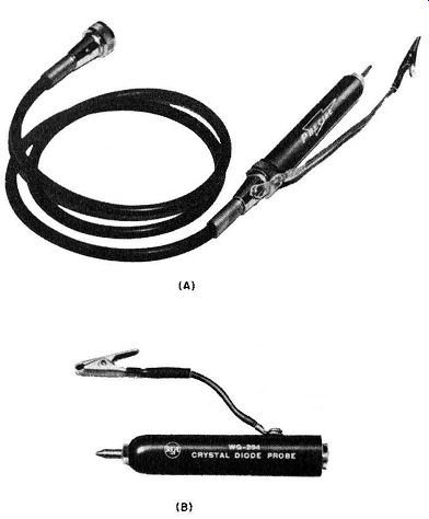
Fig. 6-23. (A) R-F crystal diode rectifying probe provided with its own shielded
cable end connector for attaching to the D-C Volts terminal of the vtvm. The
short ground lead and clip are attached to the metal end-shell. ( B) Separable
type of r-f crystal-diode rectifying probe designed to be slipped onto the
standard direct probe and shielded cable used with all models of RCA Volt-Ohmyst
vtvm's. This probe has a rated frequency range of 50 khz to 250 mhz.
Its interior construction is illustrated in Fig. 6-11. (A) Courtesy: Precise Development Corp. (8) Courtesy: RCA
The cause of these resonances is that at very high frequencies even a short length of connecting lead develops appreciable inductive reactance, which, in combination with the stray capacitance of the circuit produces series and parallel resonant conditions within the probe at various frequencies. The crystal or tube diode also has a resonant frequency, depending upon the particular type and unit employed. The magnitude of the resonance peak (and occasionally its existence) will vary with the applied voltage. For example, the percentage of error due to development of a resonant peak at 200 mhz can vary from 0 percent at 5 volts, to 10 percent at 0.5 volt, in a typical case. As a rule, the frequency at which a rectifying probe begins to exhibit resonance effects is considerably higher for a crystal-diode type probe than for a tube-diode type. If the instrument is to be used only as an indicator of the presence of, or the relative values of, r-f voltage, such resonance conditions do not limit its usefulness, and it can be used at frequencies up to and beyond those for which accurate voltage measurement is possible.
In general, use of good-quality high-frequency type capacitors and resistors, short leads, a short probe tip and a short input ground lead, careful physical layout of the components and wiring, and design of the probe head for minimum stray capacitance and minimum r-f dielectric losses (which increase with frequency), will appreciably push up the higher frequency limit to which the probe is useful for voltage measurement. Comparatively inexpensive, well-designed probes o[ this type with frequency ratings ranging up lo approximately 300 mhz arc available. More costly probes containing special design refinements arc avail able with a much higher rated useful range to approximately 3,000 mhz.
One method frequently used to increase the useful frequency range of an existing probe is to reduce its input stray capacitance by removing the probe tip and using an external small button-type high-frequency capacitor instead of the series capacitor which is ordinarily built into the tip of the probe. One lead furnished with the button-type capacitor is cut off as short as is practicable, and is used as the probe tip. The other one is connected to the center conductor of the probe.
The upper limit of frequency response when a tube-diode is used as the rectifier is also determined by transit-time action (see Sec. 6-11). When the time of transit of the electrons from cathode to anode becomes appreciable with respect to the time of a signal cycle, the input resistance of the probe falls to a low value. The higher the operating frequency, the lower is the input resistance of the probe. It is found that the effect of transit time depends upon the signal voltage as well as the signal frequency. When the anode voltage is high, the electrons travel faster, and the effect of transit time is lessened.
If a tube-diode is employed as the rectifier, use of one of the newer types of miniature diodes designed especially for operation at uhF (see Table 6-2 in Sec. 6-11) will provide a rectifier having very short electron-transit time, low anode-cathode capacitance, and a high resonance frequency.
(2) Low-Frequency Response Characteristics. At frequencies below some nominal value, depending on the effective time constant of the R-C circuit consisting of charging capacitor C1 and the load resistance, the rectified d-c output of the particular probe, and the meter indication, gradually fall off. This occurs, because at the lower frequencies the time constant becomes shorter in comparison with the time required for the applied voltage to go through one cycle (see Sec. 6-5). This attenuation can be reduced by the use of a larger value for charging capacitor C1, but this results in an increase in the physical size of the capacitor, with resultant increase in the stray capacitance to it. Consequently, the input capacitance of the probe is increased thereby and the high-frequency response will be decreased. It is evident that a compromise must be effected in the final design, depending on whether the low-frequency or the high-frequency response is the more important for the intended applications of the probe.
This low-frequency attenuation does not limit the usefulness of the instrument at low frequencies if it is to be used as merely an indicator of the presence, or relative-values, of voltages, as in signal-tracing work.
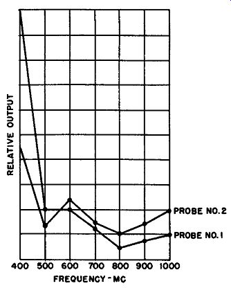
Fig. 6-24. Actual response of two typical commercial r-f crystal-diode rectifying
probes at uhf. These probes, which are designed for application in the 30-
to 300-mhz vhf range, develop sharp peaks and valleys in the response characteristic,
due to multiple resonances, and also an appreciable drop in output, when used
in the uhf range. The input impedance of such probes is also very low at uhf.
6-22. Design and Construction of Conventional Rectifying Probes
The most important considerations in the mechanical and electrical design of the probe have been discussed in Sec. 6-21, especially as regards the necessity for minimizing inductance and stray capacitances. A metal shell usually encloses and shields the rectifier and associated circuit components. (A test to determine the adequacy of the shielding is explained later m Sec. 7-16.) The ground lead from the probe should be kept as short as possible when high-frequency voltages are being measured. For low-frequency measurements, where lead inductance and stray capacitances are not quite so important, a longer ground lead, or even a longer probe tip, may be employed if these facilitate the use of the probe.
In general, ½-watt resistors will suffice for the probe, unless otherwise specified. They should preferably be of the metalized-ceramic or similar type whose distributed capacitance and dielectric losses are low, with resultant improvement in their high-frequency characteristics. It should be remembered that the effective resistance of some types of resistors decreases quite markedly as the frequency is increased above approximately 20 mhz. The capacitors also should be of the high-frequency variety having minimum inductance and losses. The resistors and capacitors should be as small in physical size as is practicable, and the layout of all parts and wiring in the r-f portions of the circuit should be such that all distributed capacitances are reduced to a minimum. Polystyrene or poly ethylene insulation should be employed on those parts which carry r-f energy, in order to keep high-frequency dielectric losses to a minimum.
Two arrangements with respect to the test cable are in common use. One provides the probe with its own test cable and end connector which must be of a type to match the D-C Volts terminal provided on the d-c vtvm with which the probe is to be used (see right-hand column of Table 1-3 in Sec. 1-4). A commercial rectifying probe of this type is illustrated in Fig. 6-23A. When d-c voltage measurements are to be made, the cable of the d-c probe (which usually contains the isolating resistor as explained in Section 4) is attached to the D-C Volts terminal of the vtvm. For r-f voltage measurements, the end connector of the rectifying probe cable is attached to this terminal instead.
In the arrangement illustrated in Fig. 6-23B, the auxiliary rectifying probe is made in separable slip-on form designed to be slipped onto the standard direct probe and cable that is used with the instrument for all d-c voltage measurements. This construction makes it unnecessary to change the probe cable connections at the vtvm when changing from d-c to r-f voltage measurement.
6-23. Rectifying-Probe Insertion Loss and Measurement Accuracy
Before undertaking to make voltage measurements with a d-c vtvm to which an external shop-constructed, or separately purchased, rectifying probe has been added, the operator should determine the attenuation factor or insertion loss introduced by the probe. This may be done by checking the scale indication of the vtvm against the value of a known source of peak, or peak-to-peak voltage, when the latter is applied to the probe input. Any such insertion loss is added to the inherent error of the instrument. For example, if a d-c vtvm whose accuracy is ±3 percent is used with a peak-to-peak probe whose accuracy is ±2 percent, the accuracy of the combination may be ± 5 percent.
The pulse-response capability of a p-p probe and vtvm combination may also have to be taken into consideration if the p-p voltage of very narrow pulses of low repetition rate are to be measured (see Sec. 6-10). For example, a d-c vtvm having an accuracy of ±3 percent may be used with a peak-to-peak rectifying probe having an accuracy of ±2 percent. Narrow pulses are applied to the input of the probe, and reference to a chart supplied by the vtvm manufacturer shows that the pulse width and pulse repetition rate are such as to introduce an error of ±2 percent. The accuracy of measurement may then be 3+2+2=±7 percent.
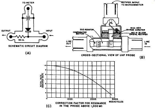
Fig. 6-25. When uhf voltages are to be measured with accuracy, it usually
becomes necessary to build the rectifying probe in the form of a coaxial-line
arrangement, as shown here. The resonant frequency of this particular unit
is approximately 3,600 mhz. The working-frequency range for voltage measurement
is 15 mhz to 2,500 mhz, subject to resonance correction above 1,000 mhz as
provided by the chart in (C). Indications of the presence of voltage and correct
voltage ratios, can be obtained at frequencies both lower and higher than this
range. The maximum voltage input rating is 2 volts. Courtesy: General Radio
Co. SCHEMATIC CIRCUIT DIAGRAM ; CROSS-SECTIONAL VIEW OF UHF PROBE ; CORRECTION
FACTOR FOR RESONANCE IN THE PROBE ABOVE 1,000 Mhz
6-24. Rectifying Probe for UHF Voltage Measurement
Well-designed conventional crystal-diode rectifying probes intended for use 10 the uhF band generally remain non-resonant "flat" at frequencies below 100 or 200 mhz, but if it is attempted to use them in the uhF region (300 mhz to 3,000 mhz) such probes develop multiple resonances resulting in sharp peaks and valleys in the frequency characteristic, and their output also decreases very appreciably, as shown in Fig. 6-24. The input impedance of a conventional probe of this type is also very low at uhf.
It is generally recognized that application of probes of conventional construction at frequencies appreciably above 100 mhz is difficult because of the attenuation, resonances, and radiation of the exposed leads. At the higher frequencies, it is almost mandatory that measurements be made on voltages which are confined to transmission-line circuits. For use in the thousands of megacycles range, the probe arrangement may be conveniently built into a coaxial line as is done in the General Radio 874-VR voltmeter rectifier illustrated in Fig. 6-25.
This arrangement consists of a short coaxial line with a 1N21B silicon crystal diode mounted in the inner conductor leading to the meter, and with a 50-ohm cylindrical resistor in series with the line inner conductor at the output end. A bypass capacitor is incorporated in the crystal mount.
The crystal rectifies the high-frequency voltage applied across the line, and the rectified output is brought out to a coaxial connector which feeds it to a microammeter that is suitably calibrated. Placed in a coaxial system, the rectifier can also be used to monitor voltage levels. The 50-ohm resistor provides an effective termination for a 50-ohm cable or line extension connected to the resistor end of the unit, so that at the far end of the cable or line extension, the open-circuit voltage equals the voltage at the crystal, less attenuation, and the effective source impedance is 50 ohms. The resistor can be replaced by a suitable metal tube if no termination is desired.
A separate voltmeter indicator is used to provide a means for measuring the voltage by a substitution method. It includes a 60-cycle circuit for calibrating the crystal at any desired level between 0.1 volt and 2 volts, so that the accuracy of the voltage measurement is independent of the crystal characteristic.
6-25. VTVM Rectifying-Probe Selection and Application Hints (1) Probe Selection. VTVM rectifying probes find wide application in making signal-generator and oscillator r-f output measurements, checking receiver stage gain, tracing signals, locating spurious oscillations, and many other servicing operations in radio, tv, and other electronic equipment. One of the first precautions to be observed in probe selection for a particular voltage measurement application is to use a peak-indicating type probe only when the peak value, or the rms value, of sine-wave voltages is to be measured. When it is desired to measure directly the peak-to-peak value of complex waveforms (or the rms value of sine-wave voltages), a peak-to-peak indicating type probe, or a positive-peak negative-peak probe, should be employed. The reasons for this are fully explained in Sec. 6-8.
The second precaution to be observed is to make certain that the maximum voltage which can be safely applied to the probe, and the frequency range throughout which its indications are reliable, will not be exceeded by the voltage under test. The maximum voltage and frequency-range ratings specified by the probe manufacturer should be ascertained and not exceeded. It should be re membered that there is no voltage divider ahead of the rectifier in a vtvm probe; the full voltage under measurement is applied to the rectifier input circuit.
Most probes which employ a 1N34 crystal diode have a maximum safe voltage rating of approximately 20v rms, 28 v peak, and 250 volts dc. Probes which employ tube diodes generally have maximum voltage ratings ranging from approximately 100 to 300 volts, depending on the particular unit. When higher r-F voltages are to be checked, an oscilloscope may usually be used more advantageously than the vtvm-plus-probe combination.
(2) Probe Application Hints. One of the most important things to be kept in mind at all times when using an r-f rectifying probe to make quantitative measurements at high frequency, is to take every precaution to make sure that the outer shell of the probe is well grounded as close as possible to the point from which a measurement is desired, or to a common ground if possible. Also, the probe tip should make contact at a point which is the nearest available one to the point whose r-f potential is to be measured.
The physical placement of the circuit components and the wiring around the measurement and grounding points should be disturbed as little as possible by the introduction of the probe tip and the grounding clip.
Do not make any conductor extensions to either the probe tip or the grounding lead when using it for high-frequency voltage measurements, because inaccuracies will result from the added inductance and stray capacitance of even a small length of wire.
The technician who has both a peak-indicating probe and a voltage-doubler (peak-to-peak) probe available, is sometimes puzzled by the apparent ability of the peak-to-peak probe to provide more than double the output of the peak indicating probe in some tests. In other tests, the peak-to-peak probe provides less than this amount of output. Such apparent discrepancies in operation of the two probes are due to the fact that the waveform of the voltage under test is not sinusoidal, and accordingly the wave has a greater positive excursion than negative excursion (or vice versa). The peak-indicating probe may be polarized so that it is measuring the smaller excursion of the voltage (or vice versa), which is less than half the peak-to-peak value (or vice versa). To make a meaningful check of a peak-to-peak probe against a peak-indicating probe, the operator should utilize a signal generator which provides r-f output of good waveform (small harmonic content). A d-c vtvm may be used with any rectifying probe as a voltage indicating rather than a measuring device. If it is desired to use it as a voltage measuring device, it is necessary that the isolating resistor used in the probe be of a correct value for proper voltage division with the input voltage divider of the particular vtvm with which the probe is to be used. Its value depends on the input resistance (including that of the d-c probe normally used with the vtvm for d-c voltage measurement) of the vtvm, as explained in Sec. 6-14.