AMAZON multi-meters discounts AMAZON oscilloscope discounts
5-1. Function of Low-Capacitance Circuit-Isolation Probes
The internal vertical-input circuit of an oscilloscope contains a certain amount of resistance shunted by capacitance. Typical normal values for five different popular makes of tv servicing scopes are: Scope A 2.0 meg shunted by approx.
B l.5 C l.0 D 0.5 E 0.1 22µµf 20µµF 30µµf 26µµf 15µµf
Thus, typical input resistances are of the order of 0.1 to 2 megohms, and typical shunt capacitances arc of the order of 15 to 30 µµf. To this input capacitance is added the approximately 30 to 50 µµf (or more) combined capacitance of the direct probe and the shielded coaxial input cable that is customarily used to minimize stray capacitance effects and spurious-voltage induction by stray fields (see Sec. 3-3 to Sec. 3-5). Consequently, whenever the test prod of a typical service-type scope, used with its conventional direct probe and test cable, is placed at some point in a circuit in order to measure the p-p voltage or check the waveform present there (see Fig. 5-1), the circuit under test is automatically being shunted by about 0.1 to 2 megohms of resistance R2, and 45 to 80 µµf (or more) of capacitance, C2, depending upon the particular make and model of scope employed.
Addition of this shunting resistance and capacitance to some circuits under going test produces virtually no noticeable effect on their operation and on the voltage and waveform present at the test point. However, in many other cases this amount of added capacitance may be sufficient to detune resonant circuits, or to capacitively load others enough to seriously distort the waveforms under observation or alter the p-p voltage values, particularly if the circuit under examination has high impedance or contains components of relatively high frequency (such as high video frequencies). For example, the input impedance presented to a video-frequency signal of say 1 mhz by a service scope and direct
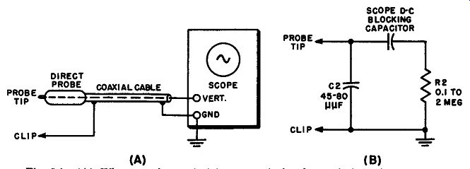
Fig. 5-1. (A) Whenever the vertical input terminals of a typical service-type
scope are connected to a circuit through its direct-probe and cable in order
to make a waveform or p-p voltage check, that circuit is being shunted, as
shown in the equivalent circuit (B), by about 0.1 to 2 megohms of resistance
and 45 to 80 µuf (or more) of capacitance, depending upon the particular make
and model of scope used.
This amount of shunting capacitance is often sufficient to detune resonant circuits or to seriously distort the waveforms under observation, particularly if the circuit under examination has high impedance or contains components of high video frequencies.
cable whose over-all input capacitance is 70 uF is approximately 2,000 ohms at this frequency. Typical of the latter group of circuits are the following in tv receivers: (1) the sync circuits; (2) the horizontal-deflection coil circuits; (3) the horizontal-oscillator circuits; (4) the composite video circuits; etc. In fact, this difficulty is experienced generally whenever it is required to scope-trace audio, video, sync, or sweep waveforms through high-impedance circuits at moderate voltages.
To prevent the overall input resistance and capacitance of the scope from causing enough circuit loading to produce these disturbing effects in such circuits, it is necessary to employ some means for sufficiently decreasing the normal input capacitance (increasing the input impedance). This may be accomplished in a simple and convenient manner by means of a compensated R-C type of circuit-isolation probe commonly known as a "low capacitance" or "high-impedance" probe because of its function.
5-2. Circuitry and Operation of Typical 10-to-1 Low-Capacitance Probes
The simplest type of conventional frequency-compensated R-C divider low capacitance probe for use with scopes is illustrated in Fig. 5-2A. A small semi variable tubular or ceramic trimmer-type capacitor, C1, shunted by high resistance R1, is connected in series with the "hot" lead of the shielded test cable to the scope, thereby placing the parallel combination in series with the overall 0.1 to 2-megohm input resistance R2, and the 45-to-80-uF input capacitance, C2, of the scope.
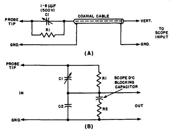
Fig. 5-2. (A) A simple type of low-capacitance probe which causes a-c signal
attenuation only. The probe capacitance C1 and resistance R1, and the overall
scope (plus cable) input capacitance C2 and resistance R2, form the resistance-capacitance
divider circuits shown in (B). The scope d-c blocking capacitor is neglected
in this consideration, because its reactance is practically zero at radio frequencies.
The complete equivalent circuit is illustrated in Fig. 5-2B. It is seen that a resistance-capacitance (R-C) divider circuit results. The d-c blocking capacitor of the scope is shown, but since it has a large capacitance and therefore a very low reactance, it may be neglected in all high-frequency a-c test signal combinations.
Since the resultant capacitance of two capacitors in series is less than that of the smaller capacitor, the effective input capacitance at the probe may be made almost any desired fraction of the overall scope input capacitance C2 by suitable choice of the value of the series capacitor C1 in the probe. The use of the series resistor R1 also reduces the effective input capacitance of the scope as explained previously in Section 4 (Sec. 4-1). Furthermore, since the two capacitors and the two resistors in series form a voltage divider for applied a-c voltages (see Sec. 2-2), and the a-c voltages which appear across the individual capacitors are in inverse ratio to the capacitances, and directly proportional to the resistances, it follows that the increase in the overall scope input impedance and the reduction of the overall scope input capacitance by a certain ratio is accompanied by a loss of a-c signal voltage (in the same ratio) entering the scope. This loss is usually referred to as the attenuation of the probe.
The series capacitor and resistor are usually chosen and adjusted to have a value which makes the attenuation ratio a convenient figure-usually 10-to-1, or 100-to-1. The 10-to-1 probe is the most widely used in tv service work (see Sec. 5-5). Since the a-c voltage-stepdown ratio is then a decimal fraction, use of the probes with a calibrated scope does not destroy the rms or the p-p voltage calibrating factor (or deflection-sensitivity rating) of the scope. A zero, or two zeros, as the case may be, is merely added to the initial calibrating factor of the scope. Thus, if the vertical deflection sensitivity of a particular scope is 0.02 volt rms (0.057 volt p-p) per inch when it is used with its direct probe and cable, it becomes 0.2 volt rms (0.57 volt p-p) per inch when it is used with a 10-to-1 low-capacitance probe.
It is evident that it is desirable that the attenuation factor of the probe be maintained practically constant for low frequencies as well as high frequencies.
Consequently, the probe must be frequency-compensated for the entire frequency range over which it will be used in practice. No waveform distortion occurs in the probe if its time constant (R1 x C1) is made equal to that (R2 x C2) of the overall scope input circuit. (The method of adjusting the series capacitor of the probe to make these time constants equal is explained in Sec. 5-8.) When the two time constants are equalized, the probe divides input voltages of all frequencies in the same proportion. An exception to this rule occurs where the voltage input delivered to the scope is increased (or decreased) by resonance (or anti-resonance) effects occurring in the shielded input cable, such as when the frequency of the a-c voltage under test is sufficiently high so that the length of the probe cable is a substantial fraction of the operating wavelength. However, this limitation docs not impair the usefulness of the probe for most service applications, because most service-type scopes do not respond to frequencies within the resonance-frequency range of the input cables supplied with most conventional low-capacitance probes.
In a 10-to-1 low-capacitance probe of the type illustrated in Fig. 5-2, the capacitance of C1 is made approximately one-ninth that of C2, and resistance R1 is made 9 times that of R2 in order to provide the 10-to-1 factor. A ± 1 percent, 1-watt carbon resistor is ordinarily employed for R1.
The practical effect of employing this type of 10-to-1 low-capacitance probe with a scope and input cable whose normal over-all input resistance and capacitance are, say, 1 megohm shunted by 75 µµf of capacitance, is to present an input circuit of 10 megohms shunted by a capacitance of only about 7.5 µµF to the circuit under test.
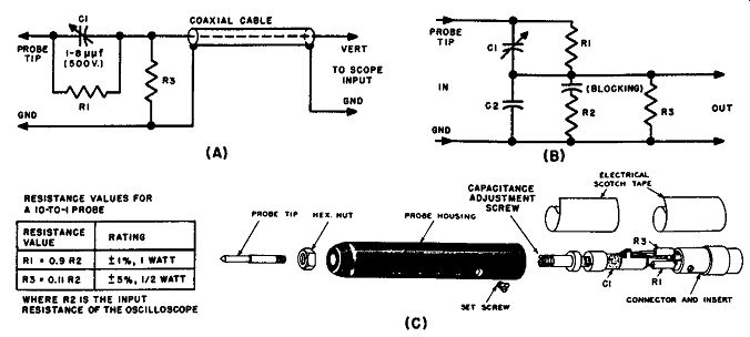
Fig. 5-3. (A) The addition of shunt resistor R3 to the simple low-capacitance
probe circuit of Fig. 5-2 serves to attenuate any d-c voltage components which
may be present at the circuit point to which the probe is touched, and which
would stress the blocking capacitor in the scope input circuit. Thus, this
low-capacitance probe provides both d-c and a-c signal attenuation, and also
stabilizes the input impedance of the scope as the vertical attenuation of
the scope is varied. The resistance capacitance divider circuit formed is shown
in (B). (C) An exploded view of this type of probe, showing the arrangement
of the components and wiring. Required adjustment of the value of series capacitor
C1 is provided by the adjusting screw which is usually reached by unscrewing
the probe tip. (C) Courtesy: RCA
Since the probe arrangement in Fig. 5-2A presents an open circuit with respect to d-c voltage (because of the series blocking capacitor which is usually present in the scope input circuit), it provides a-c signal attenuation only. Consequently, it has advantages in such uses as checking the waveform at the grid of a vertical blocking oscillator tube in a tv receiver. A high d-c bias, as well as the a-c waveform that is to be checked, exist here and the grid circuit has a high resistance. The operation of the vertical blocking oscillator depends upon the maintenance of this d-c bias, and since the grid resistance is quite large, very little input resistance can be tolerated in the scope input circuit. Therefore, it is usually found necessary in such tests to use the type of low-capacitance probe which presents practically an open circuit with respect to d-c voltage. Then, the correct bias is maintained in the high-resistance grid circuit, while the low capacitance probe reduces the effective overall input capacitance of the scope to a value low enough so that the a-c waveform is not distorted by capacitive loading of the circuit under test. This type of low-capacitance probe is usually used where there is no high d-c voltage component present at the circuit point under test.
Another version of the low-capacitance probe which is preferred for some test conditions because it provides both d-c and a-c voltage attenuation is shown in Fig. 5-3A. It is similar to the type previously described, except that it contains a shunt resistor, R3, added in the probe circuit, as shown. The resistance capacitance divider circuit which is now formed is shown in Fig. 5-3B. Observe that since resistor R3 parallels R2 and the blocking capacitor, it provides a path for d-c current flow around them. Resistors R1 and R3 form a resistive voltage divider that attenuates any d-c component which may be present at the test point. This attenuation reduces the d-c voltage that is applied to the blocking capacitor usually present in the scope input circuit, thus protecting this capacitor against excessive voltage stress that would otherwise result when testing circuits that contain a-c waveforms with a relatively high d-c voltage component. The shunt resistor also serves to stabilize the input impedance of the scope, as the vertical attenuator of the scope is varied.
One disadvantage of this circuit arrangement is that the input resistance of this probe, which is lower than that of the one in Fig. 5-2, may cause too much resistive loading of critical high-impedance circuits in which d-c is present, such as the load-sensitive grid-bias circuit of the vertical blocking oscillator previously mentioned. Consequently, it is not ordinarily used in such circuits unless a high quality blocking capacitor is connected in series with the probe tip to block the flow of d-c. This blocking capacitor is already built into some commercial probes of this type, care being taken to keep its stray capacitances very low. Its capacitance must be large enough (approximately 0.05 to 0.5 µf, high-quality low leakage paper type capacitor used) so that it will not cause low-frequency discrimination.
No waveform distortion occurs in the probe when the various resistances and capacitances are such that the following relationship exists:
R2 X R8 R1 X C1= (---) X C2 R2 + R8
It will be noted that the expression enclosed within the parenthesis here is the combined resistance of resistors R2 andR8 in parallel. Since C1 is made equal to 1/9 of C2 for a 10-to-1 probe, we have:
R2 X R8 R1 = 9 ( R2 + R8)
If R1 is made equal to 0.9R2, then a value of R8 equal to 0.11R2 must be employed. With these values in use, the input characteristics are such that the resistance presented to a circuit under test is the same as when no probe is used, but the effective input capacitance is reduced.
Fig. 5-4. (A) To measure the input resistance of a scope, first connect the vertical input terminals to any convenient low-frequency a-c voltage source, such as a 60 cycle source. Note the amount of deflection which is obtained on the scope screen.
(b) Next connect a potentiometer, or a decade resistance box R, in series with the source voltage, and adjust the value of the resistance to reduce the deflection to one-half. The value of this resistance is then equal to the value of the input resistance of the scope. (C) To measure the overall input capacitance of the scope, first connect the vertical-input terminals through the direct-probe and cable to a source of a-c voltage which has a frequency of approximately 0.25 mhz. Note the amount of deflection which is obtained on the scope screen. (D) Next, connect an adjustable series capacitor, C, (or different fixed capacitors of known values) between the scope cable and the source of 0.25-mhz a-c voltage, and adjust this capacitance value to reduce the deflection to one-half. The value of this capacitance is then equal to the value of the overall input capacitance of the scope and cable.
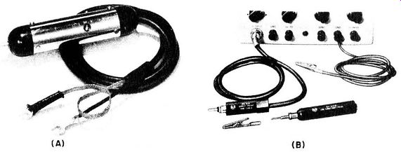
Fig. 5-5. (A) External appearance of a low-capacitance type scope probe provided
with its own shielded cable and terminals. (B) A separable type of low-capacitance
probe designed to be slipped on to the standard direct probe (with cable) employed
for several models of this manufacturer's scopes. (A) Courtesy: Hickok Elect.
Inst. Co. (B) Courtesy: RCA
It is evident that the overall input resistance R2, and capacitance C2 of a scope should be known if a low-capacitance probe is to be designed especially for it. The value of the input resistance is especially important, because the probe resistors employed usually are of the fixed type. Since the probe capacitor is the adjustable type, some leeway is allowable in the size of the adjustable capacitor that is needed.
In some cases, the input resistance and capacitance of the scope are un• known. To measure them, proceed as shown in Fig. 5-4. The determination is quite simple, provided a supply of resistors and capacitors of known and proper values is at hand.
The low-capacitance probe must be well designed to reduce to a minimum all stray capacitance between the probe tip and all components and circuit wiring on the scope side of series capacitor C1, otherwise the required low value of probe input capacitance will not be realized. An exploded view of this type of probe is illustrated in Fig. 5-3C to show the typical construction.
Many of the manufacturers of service-type oscilloscopes provide a low capacitance probe with their instruments, or make them available separately.
Some are provided with their own shielded cable and terminals, as shown in Fig. 5-5A. Another arrangement, illustrated in Fig. 5-5B, employs the separable type of construction. The low-capacitance probe shown in the foreground here is designed to be slipped onto the standard direct probe with the cable (at the left) that has been designed specifically for use with the oscilloscope. The ground cable with its alligator clip appears at the right.
5-3. Scope-Attenuator Factors Affecting Overall Frequency Response When Low-Capacitance Probe Is Used
There is more than meets the eye in the operation of a low-capacitance probe in conjunction with the input circuit of a scope, even when the scope employs the conventional frequency-compensated step attenuator in its input circuit, especially where the high-frequency response of the combination is concerned. Practical experience in the use of low-capacitance probes with scopes soon teaches the technician that hidden factors are often at work in many ser vice scopes, which not only cause peak-to-peak voltages to be indicated incorrectly when high-frequency signals of 1, 2, or 3 mhz or over are under measurement with the probe, but which often cause the high-frequency response to be unequal to the low-frequency response, thereby distorting the waveform display on the scope screen.
Fortunately, this important matter may be very simply illustrated and clarified by first considering the response of the combination at very low frequencies, and then considering the response at high frequencies, and finally comparing the two responses. The reader will recall that a standard service scope input system often comprises a frequency-compensated 3-step attenuator. The typical circuit arrangement that exists for each individual step of such an attenuator is shown in Fig. 5-6A. Capacitor C2, an internal trimmer within the scope, is used for frequency compensation, and C3 represents a fixed capacitor as well as circuit stray capacitance in the scope. These capacitances along with resistors R2 and R3 provide the required attenuation and avoid distortion in the reproduced waveform. This is a simple situation, and requires only that the product R2xC2 equal the product R3xC3. When the two time constants are made equal, no waveform distortion due to attenuator operation occurs in the reproduced pattern.
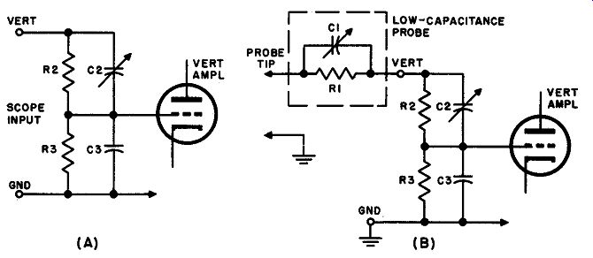
Fig. 5-6. (A) Typical circuit arrangement for one step of a simple frequency-compensated
step attenuator in a service-type scope. C2 and C3 are the frequency compensating
trimmer capacitance (in the scope) plus the fixed and stray capacitances of
the scope input circuit. The values of C2 and C3 used in each step of the attenuator
are different. (B) When a 10-to-1 low-capacitance probe is applied ahead of
the scope attenuator, the problem becomes somewhat complicated, and several
factors must be taken into consideration if correct operation is anticipated.
In practice, it is customary to make R1 = 9 (R2 + R3), since this relationship provides a basic probe attenuation factor of 10. However, the technician must re member that a commercial scope usually contains three, and sometimes four, individual attenuator steps, and these are to be accommodated by the probe. It may well be that a different value of C1 will be required for use with each step, as explained in the accompanying text.
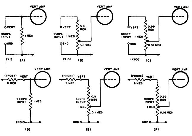
Fig. 5-7. The actions which take place in the scope attenuator at low-frequencies
present no difficulty. At these frequencies, attenuation depends solely upon
the values of the resistors in the attenuator circuit, and for this portion
of the discussion, the capacitors may be properly neglected. They are omitted
here. (A) Attenuator circuit when the gain selector switch is set for highest
sensitivity (X 1). The full voltage applied between the Vert and Gnd terminals
of the scope is applied to the grid of the vertical-amplifier tube. (8) Attenuator
circuit for X 10) position of Gain selector. It is clear that only 0.l of the
voltage applied between the Vert and Gnd terminals of the scope is being imposed
on the grid of the vertical amplifier tube, so that 10-to-1 attenuation results.
( C) Attenuator circuit (for low-frequencies) for X 100 position of Gain selector.
Only 0.01 of the. voltage applied between the Vert and Gnd terminals of the
scope is being impressed upon the grid of the vertical amplifier tube, so that
100-to-1 attenuation results.
(D) A typical 10-to-1 low-capacitance probe, with shunting capacitor neglected, provides 10-to-1 attenuation of low frequencies when the probe resistance has 9 times the value of the attenuator resistance, as shown. The step attenuator of the scope is here set for the most sensitive (X1) position. (E) This arrangement is similar to that of (D) but the step attenuator has now been set for 10-to-1 attenuation. The probe provides an additional 10-to-1 attenuation, so that the total attenuation is 100-to-1. Thus far, operation is evidently simple, and the attenuation factor is strictly correct. Of course, only low frequencies are under consideration here. (F) The step attenuator has now been set for 100-to-1 attenuation. The probe provides an additional 10-to-1 attenuation, making the total attenuation 1,000-to-1. As long as we restrict the Ohm's Law analysis to low frequencies only. the attenuation factor is still strictly correct.

Fig. 5-8. Analysis of the action of the low-capacitance probe and scope-attenuator
circuit combination at high frequencies. In some scopes the stray capacitance
C4, and designs of the step attenuator, introduce difficulties which make it
impossible to equalize the time constant of the low-capacitance probe to that
of the overall input circuit of the scope for more than one setting of the
attenuator (see text). In such cases, the frequency response of the combination
suffers when ever the scope attenuator must be set at some other position.
A somewhat obscure difficulty is encountered by the technician using a low capacitance probe in combination with such a compensated attenuator, if the attenuator in his scope was not originally designed for use with this type of probe. This circuit, with the probe connected, is indicated in Fig. 5-6B, and a simplified explanation is given in the following paragraphs, along with the requirements for obtaining satisfactory operation of a scope attenuator with the probe. It will be discovered that it is necessary, but not sufficient, that the time constant of the probe be made equal to the time constant of the scope attenuator. It is easily proven that certain relations are also required between the various capacitors.
This discussion can be simplified if the actions which take place for low frequencies, and for high frequencies, are considered separately. The low-frequency actions are illustrated in Fig. 5-7, and are explained in the caption. It can be seen that the operation of the attenuator and probe is quite straightforward, without any lurking "bugs" to complicate matters.
Let us next consider the actions which take place for high frequencies. In the high-frequency case, the attenuator resistance can be ignored since it is the relative values of the capacitances in each "step" circuit of the attenuator that determine the attenuation factor which apply for each position of the Gain selector. This is true because the reactances of the various capacitors are consider ably lower at high frequencies than the resistances of the resistors which they shunt. Accordingly, for high-frequency study, the typical circuit arrangement in Fig. 5-6A which exists for each "attenuating" position of the Gain selector switch may be redrawn as in Fig. 5-SA to avoid the complicating presence of the attenuator resistances. For the X10 position, C3 is made 9 times as large as C1 so that 0.1 of the applied high-frequency voltage is impressed upon the grid of the vertical input tube. The attenuation factor is therefore 10-to-1. For the X100 position, C3 is made 99 times as large as C2.
A low-capacitance probe is shown connected to the scope input in Fig. 5-8B. Since the high-frequency response of the probe is determined mainly by the capacitance, C1, in the probe, the probe resistance is omitted here for simplicity. If the probe is designed so that the value of C1 is made equal to 1/9 the value of the over-all input capacitive of the scope (including the cable), the probe itself will then introduce an attenuation factor of 10-to-1. If the scope Gain selector were also set for 10-to-1 attenuation, the total attenuation factor of the probe and scope would be 10x10 = 100-to-1. This much is straightforward and uncomplicated. We would need to proceed no further with such considerations, provided there were only one step in the attenuator. However, such attenuators usually contain several steps, each employing capacitances of different values. The reasons why trouble is often encountered when a low-capacitance probe is used with scopes that employ simpler types of step attenuators will now be considered.
The capacitances C2 and C3 in Fig. 5-8A and B are the total capacitances existing in the respective branches of the circuit, and they include all of the stray capacitances. The circuit of Fig. 5-8B is redrawn in part C of the same figure to show for any one step, the stray capacitance C4 which together with C5 equals C8 in Fig. 5-8B. Of course, other stray capacitances also exist in the circuit, but C4 is the most important one for our study here. It can be seen that for each "step" setting of the scope Gain control, the values of C2 or C5 which must be used so that the attenuation factor will be the correct value designated for that step, are dependent upon the value of stray capacitance C4 which exists for the particular physical circuit arrangement employed for that step.
If the scope attenuator had only one step, there would be no problem, be cause we would simply adjust the probe capacitance C1 to the value required to produce the desired 10-to-1 probe attenuation factor when used in combination with the particular values of scope cable capacitance, C2 and C5 plus C4, that happened to exist in the scope input circuit. However, in actual scope attenuators we have several steps in the Coarse attenuator to contend with. Since the circuitry for each step largely contains a separate and different physical arrangement of components and wiring, a different value of stray capacitance C4 exists for each step.
If the value of C5 in each step could be adjusted to correct for the value of C4 in that step, in conformity with the value in other steps, there would be no problem. But the technician will find that service scopes usually make no provision for correcting for the value of C4 in this way. In fact, in the simpler attenuators C5 is omitted entirely and capacitance C8 consists wholly of the stray capacitance C4 only. This is not a matter of concern in the general use of the scope when no probe is being used, because the high-frequency attenuation factor for each step may be adjusted to the correct value by attaining the required C2/C8 capacitance ratio through adjustment of C2 in that step (C2 is always made adjustable for this purpose). Unfortunately, scopes that are designed so that adjustment of the attenuation produced by each step is achieved in this all-too convenient manner usually exhibit a somewhat different scope input capacitance for each setting of the Gain selector. Because of this, when it is attempted to use a low-capacitance probe with such a scope, it is usually found impossible to equalize the time constant of the probe with that of the scope input circuit for more than any one setting of the scope Gain selector, because the different input capacitance of the scope at each Gain selector setting makes a different value of probe capacitance necessary. Frequency discrimination therefore results for all scope Gain selector settings at which the probe-scope equalization is poor. It is only a matter of chance if it is found that one probe-capacitor setting is exactly satisfactory on other than just one step setting of the attenuator. Of course, the probe can be adjusted correctly for one particular setting of the Gain control and used thereafter only with that scope setting, but this is a disadvantage in test work.
This difficulty can be overcome in the scope design by providing capacitor C5, in each step of the attenuator, and making it adjustable so that different values of C4 in each step can be compensated.
However, for practical work, it is not necessarily required that C5 be made adjustable. There is a "brute-force" design method utilized, in which capacitance C2 and C5 in each step are of the proper ratio, but they are chosen sufficiently large enough so that normal variations in the value of C4 from step to step, due to lead dress, etc., can be disregarded. One advantage to this method is that the compensator requires no attention when the vertical-amplifier tube is changed. But there is also a disadvantage in that the value of the input impedance of the scope is somewhat lower at the high frequencies than would otherwise be the case. However, one of these two methods, or some other suit able one, must be used in the scope design to avoid this trouble when a low capacitance probe is used.
5-4. Voltage Attenuation In the Low-Capacitance Probe
The attenuation of the input signal which accompanies the corresponding desirable increase in the input circuit impedance, is one of the features of the low-capacitance probe that is undesirable in some applications, but is actually required in others. It means that unless a special amplifier arrangement such as that described in Sec. 5-6 is employed with the probe, the low-capacitance probe can be used only in circuits which have sufficient signal strength so that even after the voltage attenuation caused by the probe occurs, there is sufficient signal voltage left to produce a trace of usable size on the scope screen if the gain control of the scope is advanced to the maximum-gain position. Most conventional service-type scopes have a vertical-deflection sensitivity of approximately 0.02 volt rms, or 0.057 volts p-p, per inch at full gain. When a 10-to-1 low capacitance probe is used with such a scope, 1 inch of deflection will be produced by a 0.2-volt rms, or a 0.57-volt p-p signal applied to the probe. If the signal voltage is less than this, the trace will probably be too small for accurate waveform study or p-p voltage check.
Thus, in tv service work, the 10-to-1 low-capacitance probe is generally used in waveform and p-p voltage checking in the high-impedance sync, video-amplifier output, sweep and horizontal-deflection coil circuits because these circuits provide adequate signal voltage for the use of this probe with the scope. It is often found that when the conventional 10-to-1 probe is used with a wide-band type scope, only the strongest signals can be observed on the scope because such scopes usually have comparatively low gain as a result of the special design by which their extended frequency response is achieved.
The attenuation of the input signal by a low-capacitance probe is a desirable characteristic whenever the probe is to be used with a scope for checking high-impedance circuits where the voltage exceeds the input voltage at which the scope vertical amplifier begins to distort the signal (usually around 400 volts ac rms), since it helps to reduce the voltage to a value below this limit. An example of this is furnished by the deflection-coil circuit of a tv receiver, where a p-p voltage of approximately 1,500 volts is usually present. It will be recognized that there is a basic electrical similarity between the low-capacitance probe (which is a compensated probe) and the uncompensated capacitance-divider type of high-voltage probe discussed in Section 2, because the capacitance divider action present in each of them results in a voltage step down. However; the latter type of probe is designed specifically to produce voltage stepdown, and its design is aimed at enabling it to safely withstand high voltages so that it may be used in high-voltage circuits, such as the horizontal output circuits of tv receivers. The accompanying impedance step-up that is achieved is incidental, although it is advantageous in some tests (see Sec. 2-7). The conventional low-capacitance probe is usually designed with a maximum voltage rating of only 1,000 to 2,000 volts p-p, and it must be used only in those medium-voltage a-c circuits whose voltage does not exceed this rating (see also Sec. 5-7).
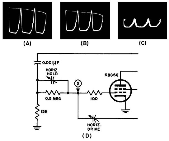
Fig. 5-9. Examples of the circuit-loading effects caused by three different
types of probes used with a scope for checking the waveform and p-p value of
the drive voltage to the grid of the horizontal-output tube in the self-oscillatory
sweep circuit of a tv receiver. The checks were made at test point X in the
circuit shown in (D). (A) The displayed waveform when a 100-to-1 low-capacitance
probe is used; 166 volts ( p-p) is indicated by the calibrated scope scale.
( B) Waveform display obtained when a 10-to-1 low-capacitance probe is used
instead (scope attenuator setting reduced); peak-to-peak value of displayed
waveform is now only 140 volts, due to increased loading of the circuit under
test. (C) Waveform display obtained when a direct probe is used (with scope
attenuator setting reduced again); waveform now measures only 60 volts peak-to-peak,
due to severe circuit loading. A voltage check made with a peak-to-peak vtvm
indicates only 55 p-p volts because of the circuit loading imposed by its built-in
rectifying net work. It can be seen that only the 100-to-1 low-capacitance
probe provides sufficiently light loading for an accurate waveform and p-p
voltage check in this critical high-impedance circuit.
5-5. The 100-to-1 Low-Capacitance Probe and its Uses in Checking Critical High-Impedance Circuits That Are Loaded by a 10-to-1 Probe
We have seen how a 10-to-1 low-capacitance probe reduces the effective overall input capacitance of a scope by a factor of 10, so that if this input capacitance is, say 75 µ,µ,f, the use of a 10-to-1 probe with the scope will reduce this to an effective input capacitance of only 7.5 µ,µ,f.
However, there are some pulse and tv waveform circuits (for example, the horizontal sync-control circuits, and the ringing coil in the horizontal blocking oscillator circuit) which are of sufficiently high impedance, or are critically resonant, so that they are adversely disturbed even by a shunting capacitance of only 7 .5 µ,µ,f. An actual example of this is illustrated in Fig. 5-9.
When the waveform or the p-p voltage in such circuits must be checked by means of a scope, it is advantageous to use a low-capacitance probe of higher ratio, such as 50-to-1, or 100-to-1, which cuts down the over-all input capacitance of the scope to 1/50, or 1/100, of its normal initial value. Thus, if the scope has 75 µ,µ,f of overall input capacitance, the use of a 100-to-1 low-capacitance probe will reduce this to only 0.75 uµf. In order to achieve the 100-to-1 capacitance ratio, the series capacitance in the probe must be made equal to only 1/99 of the overall capacitance of the scope input system. This calls for careful design of the probe. The stray capacitance between the probe tip and other parts of the circuit must be kept at a minimum.
The 100-to-1 probe multiplies the effective impedance of the input circuit by a factor of 100, and correspondingly attenuates the signal by a factor of 100-to-1. Although the voltage-attenuation factor of 100 is too extreme for purposes of general circuit testing, it is usually found that considerable p-p voltage is available at high-impedance points in sync-control systems, so that over 2 volts p-p for a trace of adequate size is still available for application to the scope after the 100-to-1 attenuation by the probe. The compensated construction assures the absence of frequency distortion within the probe at any frequency within the normal response range of the scope.
The construction details of a 100-to-1 low-capacitance probe are shown in Fig. 5-10. The probe capacitor, C1, should be adjustable, and is adjusted upon the basis of a square-wave test (see Sec. 5-8).
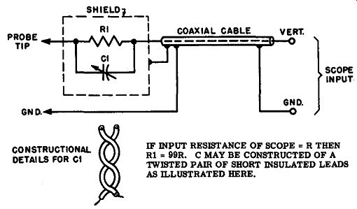
Fig. 5-10. A low-capacitance probe may be designed to produce an impedance
step-up of 100 times, as shown in the diagram here. The small capacitor, C1,
which has a value equal to approximately 1/99 of the value of the overall scope
input capacitance, is adjusted experimentally for best square-wave response
of the probe and scope at both 60 hz and at 10 or 15 khz. Because of the high
impedance step-up, the 100-to-1 probe is very susceptible to hand capacitance
and stray-field pick-up; thus the head of the probe must be of shielded construction.
The components should be adequately spaced away from the shield walls of the
probe head to avoid excessive stray capacitance from this source, which would
result in lowered input impedance.
Because the attenuation of the 100-to-1 probe is considerable, the scope must ordinarily be operated at high gain during most tests with it. If the scope has a maximum sensitivity of 0.02 volt rms per inch, its effective sensitivity is reduced to 2 volts rms per inch when the probe is used. Another solution is to employ a specially-designed amplifier with the probe, as explained in Sec. 5-6.
5-6. Use of Amplifier with High-Ratio Low-Capacitance Probes
The appreciable voltage attenuation which results when a 50-to-1, or a 100 to-1, low-capacitance probe is employed is a distinct disadvantage when using such probes in those circuits where the voltage under test is not sufficiently high to produce a scope trace of adequate size for accurate waveform study or measurement. This is especially true when a wide-band type scope is used, for such scopes have a comparatively low gain as a result of their extended Frequency response. As a result, engineering interpretation of the observed signal, with its unavoidable guesswork, is often required. However, some high-impedance or resonant high-frequency circuits encountered in electronic devices arc so critical that an extremely low value of input capacitance made possible in a well-designed high-ratio low-capacitance probe is absolutely essential when examining pulse and other type waveforms.
The obvious solution to this problem is to offset the high probe attenuation by means of an especially designed wide-band amplifier so that the overall insertion loss of the two may be reduced to zero. An amplifier for this purpose, designed to be used with the specially constructed probe shown in the fore ground at the left, is illustrated in Fig. 5-11.
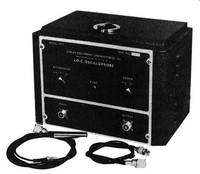
Fig. 5-11. Special amplifier for use with the high ratio ( 40 - to - 1) low
- capacitance probe shown at the lower left, so that the practical advantages
of the extremely low input capacitance of the probe ( 1.5 to 2 µ,u.f) may be
realized without the customary penalty of signal attenuation.
The adjustable overall insertion loss of the probe and amplifier combination may be reduced to zero. See Fig. 5-12 for schematic circuit diagram.
Construction details of the special probe are shown in Fig. 5-13. Courtesy: Linear Equipment Laboratories, Inc.
The circuit details are shown in Fig. 5-12 and are explained in the caption.
In general, whenever the amplitude of the test signal is unknown, it is advisable to first operate the probe amplifier at X0.01 gain setting and the oscilloscope at maximum gain when an amplifier of this type is used, permitting any overloads to occur in the oscilloscope where they are more easily recognized. If insufficient deflection is obtained, the step attenuator of the probe amplifier may then be turned to X 0.1 or X1 to increase the signal input to the scope.
The extremely low input capacitance realized with the probe employed with this amplifier results from a unique method of utilizing the stray capacitances that are inherent in a low-capacitance probe. The construction, illustrated in Fig. 5-13, is of technical interest. Observe that it is the type of low capacitance probe shown in Fig. 5-2; it contains no d-c path to ground through the probe itself. The use of a shield around the probe tip lead is necessary to avoid excessive hum voltage pickup, since this will be amplified by the probe amplifier and the scope amplifier. The application of conventional shielding here would result in a very undesirable increase in the stray capacitance across the probe input circuit. To avoid this, such stray capacitance is greatly reduced by the unique construction shown, in which the series capacitance, C1, of the probe is formed by the shielding around the input lead. The greatest portion of the stray capacitance is shunted in parallel with the overall cable capacitance which is large in any case as compared with C1. The probe is small and compact, permitting access to miniaturized circuitry. An insulating sleeve is sup plied as standard equipment, and where an absolute minimum of circuit loading is desired, the hooked probe tip may be unscrewed and the exposed button used for the input contact to the circuit under test. A special semi-air spaced low-capacitance cable is used for all interconnections, together with standard uhF connectors.
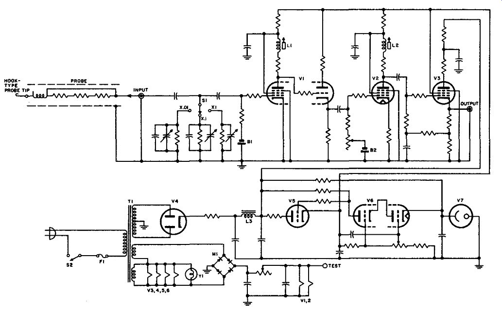
Fig. 5-12. Schematic circuit diagram of the special video amplifier illustrated
in Fig. 5-11. In order to avoid any deterioration of the signal under observation,
this amplifier is designed to have a band width in excess of that of most scopes
on the market. In addition, it must have very low noise and hum level so that
it can be run wide open when connected to the input of a high-gain scope without
causing the trace to bounce around or become distorted. To achieve this, d-c
is used on the heaters of the amplifier tubes. For stability, a fully regulated
B supply is employed to prevent jitter due to line-voltage surges. Two stages
of voltage amplification drive a cathode follower output stage. All circuits
are carefully adjusted for wide bandwidth, fast rise time, and good transient
response. The dynamic output impedance is approximately 60 ohms, and the maximum
undistorted output 3 volts rms. The input voltage range can be selected by
a three-position switch. Signals up to 150 volts rms can be applied to the
probe without overload. Input impedance on all ranges is 4.5 megohms shunted
by 1.5 uuf. Excellent response from 5 cycles to 12 mhz within 3 db is obtained.
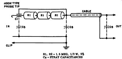
Fig. 5-13. Construction details of the special 40-to-1 low-capacitance probe
shown at the lower left of Fig. 5-11. Courtesy: Linear Equipment Labs, Inc.
This type of probe and amplifier combination is particularly useful for the examination of waveforms in critical high-impedance and resonant high-frequency circuits in color tv equipment.
5-7. Maximum Test-Voltage Limitations of low-Capacitance Probes
The conventional 10-to-1 low-capacitance probe is usually designed with a maximum voltage rating of less than 1,000 to 2,000 volts p-p, or dc. However, a probe having such a limited voltage rating can be adapted for use in the testing of low- and medium-voltage a-c circuits which have a high d-c voltage component present, by adding a high-voltage blocking capacitor in series with the probe tip.
For example, if it is desired to use a conventional 10-to-1 low-capacitance probe to check the ripple in the output from the high-voltage filter of a tv receiver, a 500-µµf 20,000-volt blocking capacitor can be used to advantage in series with the probe to avoid breakdown due to the high d-c voltage component which is present. If the low-capacitance probe is rated to withstand the ripple voltage which is present, the arrangement is satisfactory, provided proper precautions are taken when handling the probe.
Some commercial low-capacitance probes provide a 1,500-volt blocking capacitor within the probe housing. If higher d-c voltages must be withstood in certain applications, the technician can provide an additional external blocking capacitor, such as a 20,000-volt filter capacitor.
On the other hand, if the low-capacitance probe is to be used to test a circuit where the a-c voltage exceeds the rating of the probe, no advantage will be afforded by the use of the blocking capacitor, since the full a-c voltage will be applied to the probe as though the blocking capacitor were not present.
5-8. Check and Adjustment of the Time Constant and Frequency Response of the low-Capacitance Probe
In order to use any low-capacitance probe with a minimum of distortion it is necessary to adjust the value of its series capacitor so that the time constant of the probe will be made equal to that of the over-all scope input circuit (including the cable) (see Sec. 5-2), i.e., so that R1 X C = R2XC2. This adjustment is accomplished by applying a square-wave signal to the probe, and displaying the output on the particular scope which is to be used with the probe.
A square-wave signal is employed because it contains the necessary range of low-, middle-, and high-frequency components for whose frequencies equalization needs to be effected. A square-wave generator having a fast rise time, negligible overshoot, and a frequency range which includes about 30 cycles, and 15 khz should be employed. The adjustment procedure is quite simple, and is as follows: (1) Set up the square-wave generator to deliver a frequency of about 30 or 60 cycles, and feed its output to the vertical input terminals of the scope, as shown in Fig. 5-14A. Adjust the scope controls to provide a square-wave trace of two or three cycles and convenient amplitude on the screen; This test provides a check of the square-wave output of the generator and/or the frequency response of the scope. The latter is important, for the probe cannot compensate for limitations in the frequency response of the vertical amplifier system of the scope.
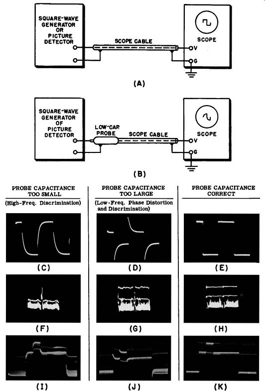
Fig. 5-14. (A), (B) Instrument setups for the two steps in adjusting the series
capacitor of a low-capacitance probe to equalize the time constant of the probe
to that of the overall input circuit of the scope and cable with which it is
to be used. A square-wave signal is employed, and the best compromise adjustment
is made for minimum distortion of the square wave as seen on the scope screen.
(C), (D), (E) illustrate the types of trace produced for various adjustments
of the series capacitor in the probe. (F) through (K) are obtained when a tv
signal is employed rather than a square-wave generator.
(2) Now connect the low-capacitance probe output terminals to the vertical input terminals of the scope; if the probe is of the separable type, slip it on to the direct probe and cable instead (see Fig. 5-5). Connect the output of the square-wave generator to the probe input as shown in Fig. 5-l4B. Increase the signal amplitude by adjusting the generator output. If the square wave obtained is now distorted as compared to the square wave previously observed, the response of the probe may be corrected by adjusting its series capacitor (by means of an insulated screwdriver) until the square wave most closely approximates the original (see Fig. 5-14C, D, E). Access to the adjustment screw of the capacitor is usually obtained through a hole in the probe or by unscrewing the probe tip from the front of the probe. If the observed waveform is considerably rounded on its leading edge, as illustrated in Fig. 5-14C, the presence of high-frequency discrimination is indicated and the capacitance must be increased by turning the adjustment screw clockwise. If the waveform is considerably pointed, as shown in Fig. 5-14D, low-frequency phase distortion and discrimination is indicated and the capacitance must be decreased by turning the adjustment screw counterclockwise.
(3) Steps (1) and (2) should now be repeated at a higher repetition rate by employing a 10- to 15- khz square-wave signal. A slight compromise adjustment of the capacitor may be found necessary and can usually be effected.
The method of checking and adjusting the square-wave frequency response of a low-capacitance probe and amplifier combination such as are described in Sec. 5-6 differs in some details from the foregoing description, and is fully de scribed in the operating instructions accompanying the instrument.
In case a suitable square-wave generator is not available, a tv receiver known to be in good working order may be used instead. Apply the probe to either the grid terminal of the picture tube, or the video detector stage. Set the scope for displaying the composite video signal, and adjust the probe capacitor so that the amplitude of the horizontal and of the vertical sync pulses are equal. As an independent check, the scope sweep can be speeded up to the picture line rate (15, 750 hz), and the horizontal sync pulse observed for rounding and tilt.
Parts F, G, and H of Fig. 5-14 show the effect of probe capacitance adjustment when a tv signal is used. In this case, the low-capacitance probe was connected to the load of the video detector and the scope was adjusted to a sweep frequency of one-half the vertical frequency. With the probe capacitance too small, the vertical-sync signal protrudes out of the video signal and the horizon tal-sync pulses are highly attenuated (see part F). With the probe capacitance too large, vertical-sync pulses are compressed and video signals and horizontal sync pulses arc exaggerated, as shown in part G of the figure. When the probe capacitance is properly adjusted, the tips of the horizontal-sync pulses (appearing as the light horizontal line above the video-signal portion of the waveform) are lined up properly with respect to the vertical-sync pulses (see part H of the figure). An even clearer representation of these effects is shown in parts I, J, and K respectively, when a 60-cycle sine-wave sweep is employed to stretch out the waveform display. Note the similarity of these effects to the square-wave traces in parts C, D, and E of the figure.
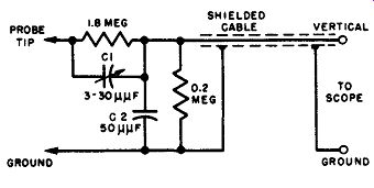
Fig. 5-15. Brute-force type 10-to-1 low capacitance probe that may serve two
or more different scopes without need for readjustment of the probe components.
Once the probe has been adjusted for proper operation with a certain scope and cable, it should be used only with that instrument and cable; it must be readjusted if used with any other instrument and cable. In fact, when used with some scopes, it may be necessary to readjust the probe if the scope Gain selector setting is changed from that employed when the original adjustment of the probe was made. This is discussed in detail in Sec. 5-3.
5-9. Brute-Force, 10-to-1 Low-Capacitance Probe for Two or More Scopes
It is occasionally desired to make one low-capacitance probe serve two or more scopes. This can be done so that no readjustment of the probe components will be required, by using the brute-force circuit shown in Fig. 5-15. This probe offers a useful increase in impedance over a direct-cable connection.
A 4-foot length of conventional RG-59/U coaxial cable having a nominal capacitance of 21 µµf per foot is used. This provides considerable input capacitance to the scope, which is increased about 50 percent by the use of the shunt 50-µµf capacitor, C2. This capacitor is added so that the trimmer, C1, may effect proper compensation. The input resistance of the scope is also "swamped" by the use of a 0.25-meg shunt resistor. Accordingly, the attenuation ratio of the probe will remain 10-to-1, within practical limits, no matter what conventional service type scope is used with the probe. Also, once trimmer C1 has been adjusted for good square-wave response with one scope (see Sec. 5-8), it will not ordinarily require readjustment when the probe is used with other scopes.
5-10. Low-Capacitance Probe Applications and Practical Operating Hints
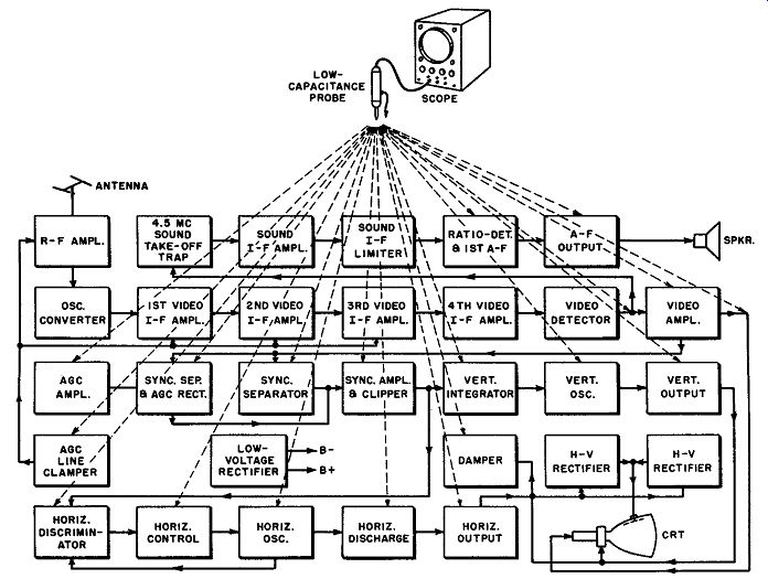
Fig. 5-16. Applications of the low-capacitance probe, use in conjunction with
a scope, for waveform checks and p-p voltage measurements in a tv receiver.
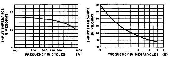
Fig. 5-17. How the input impedance of a typical low-capacitance probe decreases
as the frequency increases through the audio-frequency and radio-frequency
ranges up to video frequency ( 4 me).
Low-capacitance probes are ordinarily used in conjunction with scopes during tests made in any audio, video, sweep or sync circuits (see Fig. 5-16), in which the normal capacitance of the scope input system would detune resonant circuits, or in which the normal current drain imposed by the scope input system (chiefly capacitive shunt current) would be sufficient to noticeably load the circuit under test and thereby produce phase shift and high-frequency attenuation, with resultant waveform distortion-provided that the voltage of the circuit un der test does not exceed the maximum-voltage rating of the probe.
Although there is no waveform distortion encountered with a low-capacitance probe whose time constant is properly adjusted to be equal to that of the overall scope input circuit (see Sec. 5-8), its input impedance is not constant. As shown in Fig. 5-17, the impedance decreases somewhat through the audio-frequency range, although it is still extremely high (see part A). In the radio-frequency range, the input impedance falls rapidly, as shown in Fig. 5-17B. At low audio frequencies the input impedance may be 15 or 20 megohms in some cases, but at the upper end of the video-frequency range (4 me), it has decreased to approximately only 4,000 ohms or less. Although the latter may seem to be a very great decrease in input impedance, it must also be remembered that this amount of impedance is 8 times the 500-ohm input impedance which would be presented, at this frequency, by a service scope and direct cable whose overall input capacitance is 70 µµF. Higher input impedance at the higher frequencies may be obtained in scope tests that require it, by the use of a cathode-follower probe (see Sec. 5-11). It should be recognized that the phase characteristics and the normal frequency range of a well-designed 10-to-1 low-capacitance probe far exceed those of most service-type scopes used by tv technicians, so it may be used at 60 hz, 15.75 khz, or 4 mhz with equal facility. Accordingly, any distortion resulting at the higher frequencies will usually be localized to the vertical input and amplifier section of the scope rather than to the probe, or in the inability to equalize the time constant of the probe with that of the scope input circuit for all settings of the scope Gain selector.
(1) Use of Low-Capacitance Probe at Video Detector Output.
When a scope is connected to the output of the video detector to display the composite video signal at that point, a low-capacitance probe should be used with it. Should the technician make an error and utilize another type of probe at this point, a highly distorted version of the waveform would probably be observed.
Unless a low-capacitance probe is used at the output of the video detector when checking the square-wave response of the video i-f amplifier, the input capacitance of the scope and shielded input cable will be sufficient to seriously disturb the detector operation at the high video frequencies. Accordingly, the normal square-wave response will not be evident at higher test frequencies un less a low-capacitance probe is used.
(2) Video Amplifier Troubleshooting. Because of the wide band of frequencies handled by a video amplifier, care must be used to avoid changing its response characteristics when an oscilloscope is applied to a circuit in it for test.
Whenever possible, if the usable frequency range of the scope employed for the particular test is sufficient to make the use of a demodulator probe unnecessary (see Sec. 7-30), a low-capacitance probe should be used with the scope for video amplifier signal tracing, because of the low input capacitance and consequent negligible loading of this probe. The effect of connecting a scope which adds considerable capacitance to the video amplifier circuits of a color tv receiver is especially important, since it may disrupt the operation of the circuit so drastically that color synchronization may be completely lost.
One important typical application of the low-capacitance probe is in the testing of video amplifiers by means of low-frequency (100- khz or 500- khz) square waves (one method of video-amplifier testing). Unless the scope is applied to the picture tube grid through a properly compensated low-capacitance probe in this test, the response of the video amplifier will appear to be faulty at the higher video frequencies, because the input capacitance of the scope will load the output circuit of the video amplifier abnormally, and will round off the test square wave considerably. Of course, the scope must have adequate video frequency response for this use. In fact, the scope must have a better response than the video amplifier under test. Accordingly, if the vertical amplifier of the scope has too limited a response, the next best procedure is to apply the output from the video amplifier directly to the deflection plates of the c-r tube in the scope. In either of these procedures, the socket should be removed from the base of the picture tube, in order to eliminate this source of additional capacitance across the output of the video amplifier during the square-wave test.
(3) TV Sync-Circuit Signal Tracing. A tv station signal is almost always used in tracing sync-circuit troubles, except in some very difficult trouble cases where no signal at all can get through. Although the frequencies in the various circuits under test in the sync circuits are well within the direct response range of the scope amplifier, some of the sync circuits have a sufficiently high impedance so that application of the over-all input capacitance of the scope directly to them seriously disturbs their operation. By using a low-capacitance probe with the scope, progress of the horizontal and vertical sync pulses can be followed from the video detector (or video amplifier on through the d-c restorer, sync separator and integrating network (see Fig. 5-16). The vertical pulse can then be checked on through to the vertical oscillator, graphically revealing the operation of the pulse in triggering the vertical oscillator. A check of the effectiveness of the reactance-tube circuit in controlling the operation of the horizontal sync discriminator is another useful application of the low-capacitance probe and scope.
The important function of the low-capacitance probe in sync-circuit tests is to help the scope to achieve the effective reproduction of the various pulse shapes as they actually exist in each circuit. Waveform distortion caused by application of the scope cannot be tolerated, because the entire system of trouble shooting here is based on checking the displayed waveforms for shape and amplitude in order to determine whether or not they meet the waveform and p-p voltage specifications set forth in the servicing instructions of the receiver manufacturer.
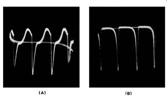
Fig. 5-18. (A) Waveform of the 1,300-volt signal appearing across the horizontal
deflection coils of a tv receiver is distorted due to scope amplifier overload,
when the direct probe and cable of the scope is applied to the test point.
(B) The true waveform is obtained when a 10-to-1 low capacitance probe is used.
The probe attenuates the input voltage from 1,300 volts to 130 volts which
the scope attenuator and amplifier are able to handle without overload.
(4) TV Sweep Circuit Testing. The grid of the vertical blocking oscillator is frequently a difficult test point, and is a good example of the application of the low-capacitance probe. The grid-leak in this circuit may have a value as high as 10 megohms. Furthermore, the waveform is sharply spiked, and the high frequency content of the waveform is easily lost if a direct connection (or a direct probe) is used. However, the low-capacitance probe reduces the test capacitance applied across the circuit to 1/10 of the value imposed by a direct probe.
As a result, the waveform displayed on the scope screen is essentially the true waveform, since the operation of the circuit is virtually undisturbed.
It should be noted that the high resistance of such circuits usually develops another source of difficulty, due to the fact that the input resistance of some low capacitance probes (see :Fig. 5-3A) causes excessive d-c bias voltage drain-off. Use of a blocking capacitor in series with the probe tip avoids this disturbance by preventing drain-off of the d-c bias voltage.
(5) Use to Prevent Scope Overloading. Although the chief function of the low-capacitance probe is to provide low input capacitance for scope applications and thus minimizing circuit loading and detuning effects, the 10-to-1 probe can also be used somewhat in tv troubleshooting procedures on the basis of its 10-to-1 voltage attenuation factor. In some tests, the peak-to-peak voltage may be a medium-high voltage which, even though not high enough to damage the scope input circuit, will cause the vertical amplifier of the scope to be overdriven, and the waveform developed on the scope screen will be distorted accordingly. Use of a 10-to-1 low-capacitance probe will attenuate such voltages down to the lower values which arc well within the voltage-handling capability of the scope amplifier.
An example of overload of the vertical amplifier of the scope when a 10 to-1 attenuating probe is not used in a medium-high voltage circuit is shown in Fig. 5-18. In this case, the distorted waveform in Fig. 5-ISA was observed when a service scope was applied directly across the horizontal-deflection coils in a tv receiver. Although the coarse Gain selector of the scope was backed off to the (X0.01) position, the input voltage was not attenuated sufficiently to avoid amplifier overload. As a result, the vernier attenuator in the cathode circuit of the cathode-follower input stage could not be used to avoid overload, although it kept the pattern on-screen. The overload was occurring in the grid circuit of the cathode-follower input stage.
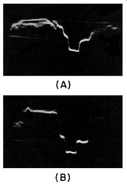
Fig. 5-19. Effect of improper adjustment of the receiver controls when waveform
checks are being made. (A) A horizontal sync pulse as it appears at the grid
of the picture tube in a tv receiver, when the contrast control is adjusted
for linear (Class A) operation of the amplifiers. (The shape of this sync pulse
is not as good as is customarily observed in some tv receivers.) ( B) The same
pulse when the contrast control has been advanced into the region of non-linear
operation. More output is obtained, but the waveform has undergone distortion;
the illustration shows incipient distortion, before severe clipping starts. The
chief distortion introduced by the non-linear operation at this particular level,
is a change in the shape of the back porch which is now convex in shape as contrasted
with its concave shape shown in (A) when the operation is linear.
When a 10-to-1 low-capacitance probe was used, the waveform appeared undistorted as shown in Fig. 5-ISB. The 10-to-1 probe attenuated the 1,300-volt signal to 130 volts, which could be handled by the coarse attenuator satisfactorily, so that the grid of the cathode-follower input stage of the scope was not over-loaded. Additional discussion of this subject appears in Sec. 5-4.
(6) Effects of Improper Receiver-Control Adjustments
When Waveform Checks are being made. Just as the scope controls must be properly adjusted to avoid the possibility of limiting or clipping the input signal and thereby obtaining a false waveshape on the scope screen, so must the receiver controls be suitably adjusted to avoid limiting or clipping in the receiver amplifiers while the waveform checks are being made. An illustration of this waveform compression appears in Fig. 5-19A and B. Accordingly, the technician must not only determine that the scope is operated correctly, but also that the controls of the receiver under test are properly adjusted. Otherwise, the receiver circuits would be incorrectly adjusted in an attempt to compensate for an observed distortion which would not be present during normal operation.
(7) Abnormal Displays may be obtained with Low-Capacitance Probes.
Because the low-capacitance probe is not a rectifying probe, the technician is sometimes puzzled by the abnormal type of display shown in Fig. 5-20 which was obtained when the output from a sweep-frequency generator was applied directly to the probe. Similar types of displays are obtained when the output from a sweep-frequency generator is applied to a direct probe. While it is true that the output from an i-f or r-f sweep-frequency generator (at least in normal operation) consists of high frequencies to which the scope cannot respond directly, it must be observed that cable resonance which occurs at certain high frequencies causes resonant rises of voltage at these frequencies. As a result of the resonant rise of voltage, the input stage of the scope becomes overloaded at the resonant frequencies, and during this condition of non-linear operation, the stage rectifies as well as amplifies. Hence, an unexpected pattern is seen on the scope screen.
(8) Application of Low-Capacitance Probe for Display of Current Waveforms. Finally, it should be observed that a low-capacitance probe can be used in connection with the display of current waveform on the scope screen, as well as voltage waveforms. In order to display the waveform of a current in a circuit, a small resistance, R, is connected in series with the circuit under test, and the low-capacitance probe is applied across the resistance, as shown in Fig. 5-21.
The resistance should be made as small as possible consistent with producing a scope trace of adequate size, in order to avoid circuit disturbances. The technician does not often have occasion to investigate current flow, but it is important to recognize that this can be done when necessary.
In all applications of low-capacitance probes it should be remembered that their use cannot extend the frequency response of the test instrument. Distorted waveforms seen on an oscilloscope, therefore, are not improved by the addition of a low-capacitance probe if the distortion is originating in the scope circuits due to overload, rectification, etc. The full value of the probe can only be realized when the response of the scope with which it is used does not impose any limitations on the test being made.
5-11. The Cathode-Follower Type Circuit-Isolation Probe
Another type of circuit-isolation probe which, in shop-constructed form, has been used to a considerable extent in laboratory work, consists of an r-f cathode-follower arranged in probe form. The schematic circuit diagram of a probe of this kind designed to be used with, and powered by, the service-type oscilloscope of the manufacturer is shown in Fig. 5-22. It will be recognized as a cathode-follower circuit, the output being taken off across the 750-ohm cathode resistor.
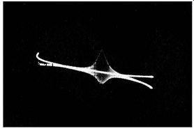
Fig. 5-20. Abnormal displays are sometimes obtained on the scope screen when
a low-capacitance probe is being used.
For example, because the shielded input cable to the scope becomes resonant at certain high frequencies causing resonant rises of voltage at these frequencies with con sequent rectification occurring in the scope input stage, the unexpected pattern shown here may appear on the screen when the high-frequency output from a sweep generator is applied to a low-capacitance probe.
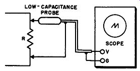
Fig. 5-21. A low-capacitance probe and scope may be used to display the waveform
of the current in a circuit by connecting a small resistance in series with
the circuit and applying the probe across the resistance.
The basic characteristics of a cathode-follower are that its grid-input capacitance is extremely low (in comparison with that of a conventional amplifier), and the input resistance is very high. Consequently the input impedance is high, even at comparatively high frequencies. A well-designed cathode-follower type of circuit-isolation probe can be built to provide a higher input impedance with less attendant attenuation than is obtained with the simpler conventional low capacitance probe. Since it has excellent high-frequency response it is recommended for circuit-isolation use in testing high-impedance circuits whenever the test frequency is a determining factor.
Since its output impedance is lower than its input impedance, the cathode follower is in a sense an impedance transformer. The voltage attenuation resulting from its use is much less than that of a comparable conventional low-capacitance type probe; this is an important advantage in low-level circuit testing.
The cathode-follower probe of Fig. 5-22 is shown in commercial form in Fig. 5-23. A type 5703 sub-miniature tube is employed. The impedance of this probe has the high value of 6.2 megohms shunted by approximately only 8 µµf.
This provides extremely low circuit loading, which is an absolute necessity in the servicing of some circuits of color tv receivers and very desirable in the servicing of some of those in monochrome tv receiver servicing. The attenuation ratio of the probe is only 2-to-1.
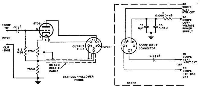
Fig. 5-22. Schematic circuit diagram of 10-LCP cathode-follower type of circuit
isolation probe which features a high input impedance, and comparatively low
attenuation factor. Courtesy: Jackson
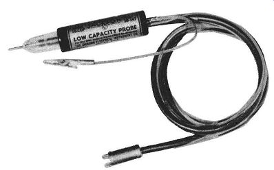
Fig. 5-23. The cathode-follower type probe whose circuit diagram is illustrated
in Fig. 5-22. Observe the probe output plug designed to fit into the special
input-circuit connector provided on the scope with which this probe is designed
to be used. Courtesy: Jackson.
The problem of providing heater and plate voltage supply for this particular cathode-follower probe has been solved by providing the scope with which it is to be used with a special shielded input connector (see Fig. 5-22) in place of the conventional Vert.-Input and Ground terminals. This connector supplies the necessary heater and plate voltages, and the scope vertical-input connections to the probe. The probe is provided with a special composite cable and 5-pin plug (as shown in the two illustrations) which fits into this connector. The 6.3-volt heater voltage for the probe is thereby automatically taken from the scope heater circuit, and the plate voltage is taken from the low-voltage power supply of the scope. The latter voltage is dropped to the proper value required by the probe tube by means of resistor R, and it is well filtered by 8-d, 450-v, electrolytic capacitor C2 and the 0.05-µf, 400-v, paper-type high-frequency bypass capacitor C3. These three components are located within the scope. The hot lead in the output cable of the probe is the inner conductor of a low-capacitance coaxial cable; the shield of this cable serves as the ground conductor and also as one leg of the heater-supply circuit (see Fig. 5-22). A cathode-follower probe is sometimes used to precede a crystal demodulator probe in order to present a much higher input impedance to the circuit under test than would be presented by the crystal demodulator probe alone. This results in decreased circuit loading which is required in some applications of de modulator probes.