AMAZON multi-meters discounts AMAZON oscilloscope discounts
Undoubtedly the best-known semiconductor device is the transistor. It was discovered
in 1945 at the Bell Telephone Laboratories by John Bardeen and W. H. Brattain;
since then it has revolutionized the electronics industry. There are many
different types of transistors, each with characteristics that make it best
suited for a particular application.
The basic difference among transistor types is the method of construction. The two main types of transistors are germanium and silicon. The basic semiconductor material in one type is germanium, and in the other type it is silicon. The economics of the manufacturing process usually determines which type of semiconductor material is used. Some manufacturing methods work best with germanium, and others work best with silicon. A few methods are suited to both materials.
There are two configurations for transistors--the NPN and the PNP. These two configurations complement each other. The existence of complementary transistor types makes possible many circuits that were not feasible with vacuum tubes. A PNP transistor can be replaced with a similar NPN; and the circuit can be made to function exactly the same, merely by reversing the polarity of the power supply. The only difference between complementary NPN and PNP transistors is the direction of current flow.
The schematic symbol for a transistor dates back to the first transistors constructed at the Bell Labs. These were known as point-contact transistors. The emitter and collector were fine wires placed very close together on the surface of a semiconductor material called the base.
The emitter has the arrow on it, signifying the emitting of current carriers into the base region. The collector is so called because it is thought of as collecting the current carriers emitted by the emitter.
Only a few types of point-contact transistors are still manufactured, and these are only for very special applications. A large majority of the transistors used today are of the junction type. For this reason, we will not consider point-contact transistors, since their operation is very similar to that of junction-type transistors.
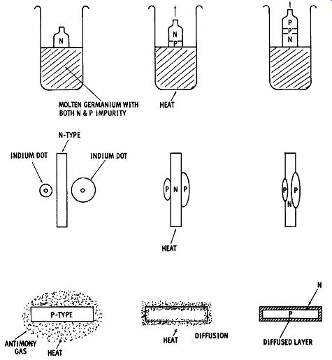
Fig. 1. Transistor manufacturing methods.
CONSTRUCTION
There are a number of ways to manufacture transistors, and each method has certain advantages and disadvantages. Transistor junctions may be manufactured in one of three basic ways-rate growing, alloying, and diffusion. Sometimes these three ways are combined to form special transistors. The basic principles of these three methods are illustrated in Fig. 1. Junctions may be grown out of a melt of the molten semiconductor material. As a germanium crystal is slowly pulled out of the melt, the crystal will grow. The melt contains both N- and P-type impurities, and whether an N- and P-type crystal forms depends on the rate at which the crystal is grown. Rate growing is not used for making either PNP or NPN silicon transistors; because of the high cost of manufacture, they cannot be competitive with the germanium transistors made in the same way.
Alloying may be likened to welding, where a junction is made between two metals by the application of heat. The alloy transistor is constructed by applying two impurity dots to the opposite sides of a semiconductor wafer and then supplying enough heat to alloy the two...

Fig. 2. Alloy transistor construction.
...dots to the wafer. Fig. 2 shows the geometry and mounting of the alloy-type transistor. The collector dot is made larger than the emitter because the emitted current carriers tend to spread out. In this way, all or most of them are collected. Both PNP and NPN germanium and silicon transistors are made by the alloying method.
Diffused mesa transistors get their name from their physical construction (Fig. 3). The collector is a flat wafer of P-type material into which a mesa of N-type material is diffused. This forms the collector base junction. A gold strip is used to make contact with the base. An aluminum contact makes up the emitter and emitter contact.
The aluminum strip on the N-type base forms a junction of dissimilar metals which has a diode characteristic. Therefore, it functions as both emitter and emitter contact. The physical mounting of the mesa transistor is shown in Fig. 3.
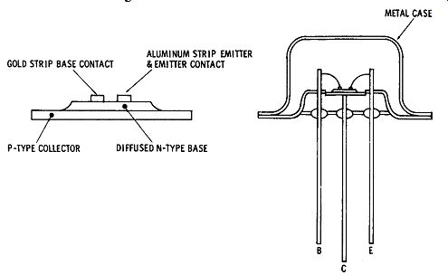
Fig. 3. Mesa transistor construction.
Transistor manufacturers found that they could get better electrical characteristics from some transistors if a collector with two different doping levels, or resistances, was used. To do this, films are grown on existing collectors, as shown in Fig. 4. These are called epitaxial ...
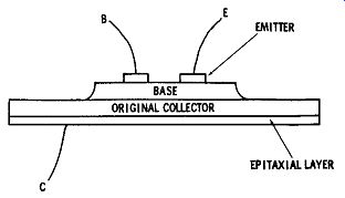
Fig. 4. Epitaxial-mesa transistor.
... films, and transistors with this feature are called epitaxial transistors.
Epitaxial means that the crystal structure of the film is lined up with the crystal structure of the collector material.

Fig. 5. Planar-passivated transistor.
Planar transistors are made entirely by diffusion, and a silicon material is always used. The name planar is derived from the fact that all of the connections ( E, B, and C) are on the same plane ( Fig. 5). A major advantage of this transistor is that the junctions are covered with silicon dioxide ( Si O), an inert material that protects the junctions from the corroding effects of the atmosphere. Thus the transistor is said to be "passivated," or protected. An oxide coating forms easily on the silicon surface, passivating it, and thus accounting for the exclusive use of silicon for this type of transistor.
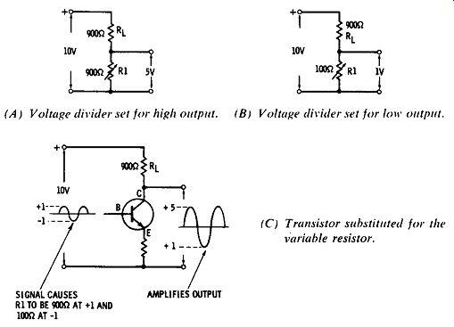
Fig. 6. Amplifier analogy.
TRANSISTOR AMPLIFIER
To accomplish amplification using a transistor, you need only to cause the transistor to operate as a variable resistor. Before continuing, let us investigate what is meant by amplification. Consider the voltage divider in Fig. 6. The top resistor is known as the load resistor ( RL), and the variable resistor (R1) represents the transistor. The variable resistor is capable of changing resistance from 100 ohms to 900 ohms.
When R1 is set to 900 ohms, there will be exactly half the voltage at the output, as shown in Fig. 6A. Since both RL and R1 are equal, there will be 5 volts across each resistor, and therefore the output voltage will be 5 volts. When the variable resistor shown in Fig. 6B is set at 100 ohms, its value equals one tenth of the total resistance.
This means that one tenth of the total voltage will appear across the variable resistor and, therefore, across the output. The output voltage in this case would be 1 volt. Consequently, by varying the resistance of the variable resistor from 100 ohms to 900 ohms, it is possible to make the output voltage change from 1 volt to 5 volts, a total change of 4 volts. Now, if you substitute a transistor for the variable resistor, as shown in Fig. 6C, and apply a 2-volt peak-to-peak sine wave to the base, the resistance of the transistor will vary. If the resistance in the transistor changes from 100 to 900 ohms, the output will swing from 1 to 5 volts. We have made a 2-volt peak-to-peak input result in a 4-volt peak-to-peak output. This device would have a gain of 2; the output is twice the input.
By applying a signal to the base of a transistor, we can cause the resistance of the transistor to vary. We can also design the associated circuitry so that the output voltage will change by a greater amount than the input voltage, thus resulting in gain. The bias battery shown in Fig. 7 is used to maintain forward bias on the emitter junction in order that the transistor can operate on the linear portion of its characteristic curve.
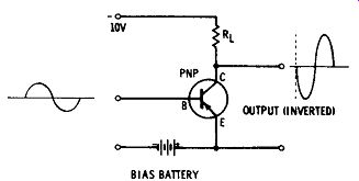
Fig. 7. PNP transistor amplifier.
The forward bias changes in synchronism with the input signal. Thus, current carriers in the base-emitter region will follow the input signal.
In the PNP transistor amplifier of Fig. 7, when the input signal is at a maximum, the current carriers will be at a minimum. When the input signal is negative, the current carriers will be at a maximum. The reason is that the input signal adds to the bias voltage. When the input is positive, it is subtracting from the bias and there are fewer current carriers.
This accounts for the inversion of the output ( Fig. 7). ( The output goes negative when the input goes positive.) Current carriers entering the base region are conducted to the collector; and since the number of current carriers varies in synchronism with the input signal, the resistance of the transistor varies in synchronism with the input signal.
Amplifier Biasing Methods
All transistor-biasing methods are based on the rule that the emitter junction should be forward-biased and the collector junction should be reverse-biased to provide linear transistor amplification. This is an important point to remember when analyzing, building, or servicing transistor circuits.
The amplifier in Fig. 7 has a disadvantage in that it employs a separate biasing battery. This is expensive and bulky, particularly since it is possible to use the supply battery to provide bias (Fig. 8). In this case, a resistor replaces a battery at quite a saving in cost and space.
R1 is a biasing resistor; current from the battery flows through R1 and through the emitter base junction, thus providing forward bias. The amount of bias depends on the resistance of R1. The collector junction is reverse-biased by the positive voltage applied to the collector through load resistor R1,. Transistors are very sensitive to changes in temperature. In fact, as the temperature increases, the number of current carriers increases and the resistance decreases. Consider Fig. 8; bias current flowing in the emitter circuit causes collector current to flow, and this collector current causes the transistor to heat. As the transistor heats, more current flows in the circuit because of the temperature dependence of the transistor. This action, which may continue to the point where the transistor destroys itself, is called thermal runaway. Destruction does not always occur; the transistor normally does not get too warm because the heat is radiated, or carried off, by air currents in the unit. However, thermal runaway is a serious problem.

Fig. 8. NPN transistor amplifier.
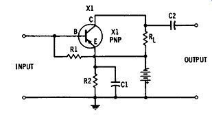
Fig. 9. Emitter resistor used to stabilize a transistor amplifier stage.
A circuit for stabilizing a transistor amplifier against thermal run-away is shown in Fig. 9. An emitter resistor (R2) is placed between the emitter and ground. If the transistor begins to heat, the increased current in the collector circuit causes an increased voltage drop across R2. As a result, voltage on the emitter rises, reducing the forward bias on the base. As a result, less current flows in the emitter junction. This, in turn, reduces the collector current and permits the transistor to cool.
The capacitor across emitter resistor R2 is called an emitter bypass capacitor; it is used to maintain the emitter of the transistor at AC ground.

Fig. 10. Stabilized transistor amplifier.
The circuit of Fig. 9 may be further stabilized against changes in operating characteristics due to changes in temperature. This is done by insertion of R3, as shown in Fig. 10. R3 provides more reliable and more stable operation of the transistor amplifier by holding the base voltage constant, regardless of changes in the transistor parameters due to changes in temperature. R1 and R3 may be thought of as a voltage divider that keeps the base voltage constant. R2 keeps the emitter voltage constant. The only disadvantage is that this circuit draws more current from the battery than either of the previous circuits; however, the additional stabilization is worth the extra current drain on the battery.
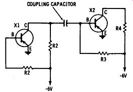
Fig. 11. Capacitive-coupled transistor amplifier.
Coupling Methods
To provide increased gain, most transistor circuits require that two or more amplifiers be cascaded. The output of one amplifier is fed into the input of the next amplifier and amplified, until the desired output level is reached. One of the most common types of coupling is capacitive coupling. The amplifier shown in Fig. 11 uses capacitive coupling. The purpose of capacitor C1 is to block the DC voltage at the collector of the transistor and to pass the AC signal. This DC voltage must be blocked because it would upset the biasing of the next stage.
Capacitive coupling of transistor stages is the most economical but not the most efficient method. The reason is that each transistor amplifier has different input and output impedances. Usually, capacitive coupling does not afford an efficient impedance match between stages. As a result, the signal coupling is not as good as it could be.
The most favorable condition for signal transfer exists when the output impedance of one stage is matched to the input impedance of the next stage. Impedance is a specific name for AC resistance. A trans former is used as an impedance-matching device between transistor stages. Fig. 12 shows a transformer-coupled amplifier. The load resistors of the amplifiers are replaced by the primaries of the transformers. C2 blocks the DC bias current for X2 from returning to ground, and it also provides an effective AC ground for the secondary of transformer T1. If C2 were not in the circuit, the series resistance of bias resistors R4 and R6 would reduce the level of the applied signal.

Fig. 12. Transformer-coupled transistor amplifier.
The AC signal is coupled from the primary of the transformer to the secondary. The disadvantage of transformer coupling versus capacitor coupling is the higher cost of the transformer. Sometimes, however, the added expense is justified.
Unlike vacuum tubes, transistors are available in complementary types, NPN and PNP. Transistors may be direct-coupled using opposite transistor types, PNP and NPN, as shown in Fig. 13. The first stage is a PNP transistor amplifier. The second stage is an NPN amplifier that is direct-coupled to the previous stage. Transistor X2 receives bias current from the load resistor of the previous stage. The emitter resistor (R6) of transistor X2 is returned to the negative terminal. Also, load resistor R6 for the NPN transistor (X2) is returned to positive. This, in effect, turns the power supply around for use with the NPN stage.
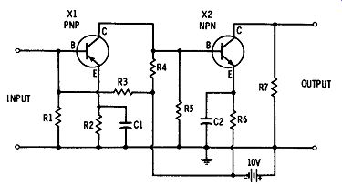
Fig. 13. Direct-coupled transistor amplifier.
It is direct-coupled and takes advantage of the complementary symmetry of NPN and PNP transistors.
AMPLIFIER CONFIGURATIONS
Up to now we have been discussing what is known as the common emitter amplifier configuration. There are two other ways to operate a transistor as an amplifier-the common-base and the common collector configurations. The word "common'' is sometimes used inter-changeably with "grounded." It refers to the element that is common to the input and output circuits. The common-emitter circuit is probably the most popular because it provides good voltage, current, and power gain.
Common-Emitter Amplifier
Common-emitter amplifiers are shown in Figs. 8 and 9. The base of both the PNP and NPN types is referenced to ground. This base becomes one of the terminals in the input circuit and also one of the terminals of the output circuit of a common-emitter amplifier.
Common-Base Amplifier
Fig. 14 shows a common-base circuit. The input signal is fed into the emitter and drives the base junction. An amplified version of the driving signal flows in the collector circuit. Note that there is no inversion in the common-base amplifier as there is in the common emitter.

fig. 14. Common-base amplifier.
The voltage gain of a common-base amplifier is lower than that of a common-emitter amplifier. The common-base amplifier does, however, afford a large degree of current gain and isolation between the input and output circuits. For this reason, it is often used for amplifying high frequency signals where stability is desired. Note that even though this configuration differs greatly from the common emitter, the emitter junction is still forward-biased and the collector junction is still reverse biased. The vacuum-tube counterpart of the common-emitter circuit is the grounded-grid amplifier.
Common-Collector Amplifiers
The third circuit configuration is connected so that the collector is common to both the emitter input and the base output circuit ( Fig. 15). A common-collector circuit is often referred to as an emitter follower. The counterpart in vacuum-tube circuitry is the cathode follower. The reason for the name "emitter follower" is that the voltage across the emitter resistor tends to follow the base voltage, in the same way that the cathode voltage follows the grid voltage in a...
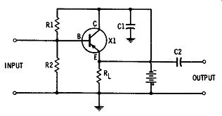
Fig. 15. Common-collector amplifier.
...cathode follower. The load resistor (Rd in Fig. 15 is in series with the emitter. Note that the collector is connected directly to the battery negative. The purpose of C1 is to ground the collector to AC signals.
The voltage gain of an emitter follower is always less than 1. It is therefore not of much use as a voltage amplifier. The power gain is greater than 1, but less than that of other configurations. You might ask why the emitter follower is used at all. The reason is that it has a very high input resistance, a very low output resistance, and good current gain. Signal transfer between circuits is very sensitive to the resistance of both the circuits into which they feed and the circuits which feed them. An amplifier stage working into the proper or matched load resistance may have a gain of 500, whereas the same amplifier working into an unmatched load resistance may have a gain of only 50. The emitter follower is commonly used as a resistance, or impedance matching, device.
Tuned Amplifier
Often, in electronics, amplifiers are used to amplify one frequency.
Such a circuit is called a "tuned" amplifier. This means the amplifier is tuned to a specific frequency and it amplifies only this frequency, excluding all others. In the tuned amplifier the input circuit, output circuit, or both, employ tuned circuits that are generally composed of inductive and capacitive elements. Fig. 16 shows a simple tuned amplifier. If a tuned circuit is placed in the collector circuit of a transistor amplifier, as shown in Fig. 16, the circuit will, for all practical purposes, amplify at the resonant frequency of the tuned circuit. Other input signal frequencies are not amplified. This type of circuit makes it possible to select and amplify one particular frequency, or a group of frequencies. The signal is inductively coupled from the output of one stage to the input of the next by a method called transformer coupling.
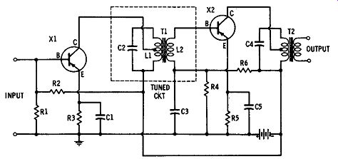
Fig. 16. Tuned amplifier.
OSCILLATOR CIRCUITS
An amplifier circuit oscillates when some of the output is fed back to the input in such a way that the amplifier becomes unstable. At first glance, one would think that this would be an undesirable condition.
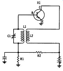
Fig. 17. Tuned-base oscillator.
Sometimes it is; however, oscillators are used to accomplish very important functions, such as the generation of signals that act as carriers for radio-communications.
Fig. 17 shows a very simple feedback oscillator. The output signal is coupled back into the input base circuit through the transformer comprised of coils L1 and L2. L1-C1 is a tuned circuit that determines the frequency of the oscillator. Energy from coil L1 is fed directly to the base of the transistor. As the collector current rises, the feedback causes the transistor to conduct more heavily, and the output current rises faster. When the collector current reaches the point where it can rise no more, the base signal begins to decay. This flywheel effect produces an output having a frequency that is determined by the values of L1 and C1.
This type of oscillator is called a tuned-base or common-emitter oscillator. The resonant elements can also be placed in the collector or emitter circuits. The frequency of an oscillator is always determined

Fig. 18. Colpitts oscillator.
by the resonant frequency of the tuned circuit. Two other types of oscillators, the Colpitts and the Hartley, are shown in Figs. 18 and 19. The Colpitts oscillator feeds a portion of the output back to the input through a capacitive voltage divider ( C2 and C3). The combination of C2, C3, and L1 makes up a tank circuit that determines the frequency of the oscillator. C2 and C3 are variable, and they determine the frequency of the oscillator. In the Hartley oscillator ( Fig. 19)
some of the output signal is fed back to the input from an inductive voltage divider ( L1 and L2). C2 is variable, and its setting determines the frequency of the oscillator. These are the types of oscillators that are generally found in the high-frequency circuits of radio and TV equipment.
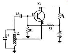
Fig. 19. Hartley oscillator.
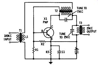
Fig. 20. Transistor converter stage.
FREQUENCY CONVERTERS
Very often it is desired in electronics to convert one frequency to another. For example, in a standard radio receiver the incoming radio frequency (RF) carrier is converted to a lower intermediate frequency (IF). The process of doing this is called frequency conversion, mixing, or heterodyning. The last of these terms accounts for the name "super heterodyne" applied to radio receivers.
All mixers and converters are based on the fact that when two signals of different frequencies are mixed, many other frequencies are generated. One is the sum of the original frequencies; another is the difference. For example, if the two input frequencies to a mixer are 100 khz and 75 khz, there will be four output frequencies, the two original, plus the sum and the difference frequencies. These are 100 khz, 75 khz, 175 khz, and 25 khz.
To change 100 khz into 25 khz, a separate oscillator (local oscillator) would be used to generate a 75-khz signal. This would be mixed with the 100-khz input. A resonant circuit tuned to 25 khz and placed across the output would pick out the desired signal and reject the three other components, resulting in an output of 25 khz. It is possible to perform frequency conversion with one stage. Fig. 20 shows a practical converter circuit of the type that is often found in transistor radios. If the RF input is 100 khz and the circuit oscillates at 75 khz, the output will be 25 khz. Transistor X1 oscillates by virtue of the feedback from T2 to the base input circuit. C2 and L2 are tuned so that the circuit oscillates at 75 khz. The 100 khz is fed in through transformer T1 and mixed with the 7 5 khz in the base circuit. All four frequencies (100 khz, 17 5 khz, 7 5 khz, and 25 khz) are available in the collector circuit. C3 and L3 are tuned to 25 khz, and this frequency is present at the output of transformer T3.
AUDIO OUTPUT STAGES
After an RF signal has been amplified and detected, it is applied to an audio output stage. The most common example is shown in Fig. 21, a typical single-transistor, power-output stage. Notice that the power transistor is biased by resistors R1 and R2 in the same manner...

Fig. 21. Single-ended output stage.
...as other transistor amplifiers. Fig. 22 illustrates a push-pull output stage. Each transistor amplifies half of the input signal; since each transistor has to work only each half cycle, it can be driven harder, thus providing an efficient output stage. The R1-R2 voltage divider provides a small amount of forward bias for X1 and X2. The secondary of T1 is center-tapped to provide opposite polarity signals for the base of transistors X1 and X2. Thus, when X1 is going positive, X2 is going negative, providing push-pull operation. The major disadvantage of ...
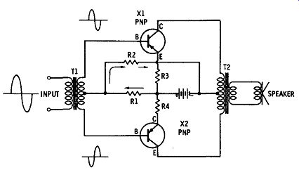
Fig. 22. Push-pull output stage
... this circuit is the need for transformers to split the polarity of the input signal and to couple power to the speaker.
The output transformer may be eliminated from a push-pull output stage because of the low impedance of power transistors. Fig. 23 shows a diagram of a push-pull output stage that employs complementary transistor types. R1, R2, and R3 form a voltage divider to forward bias transistors X1 and X2. When the input signal goes negative, transistor X1 drives the speaker in one direction; on positive signals, transistor X2 drives the speaker in the opposite direction. In this output...
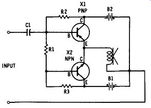
Fig. 23. Transformerless output stage.
...stage the complementary transistors make it possible to eliminate both the driver transformer and the output transformer.
PRACTICAL RADIO RECEIVER
When a relatively complicated circuit is being discussed, it is useful to employ a block diagram, such as the one shown in Fig. 24. Each stage is represented by a labeled block, and the signal paths and the direction of the signals are indicated by arrows. The signals present at the output of the various stages are also included for easy reference.
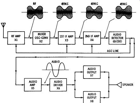
Fig. 24. Block diagram of a broadcast receiver.
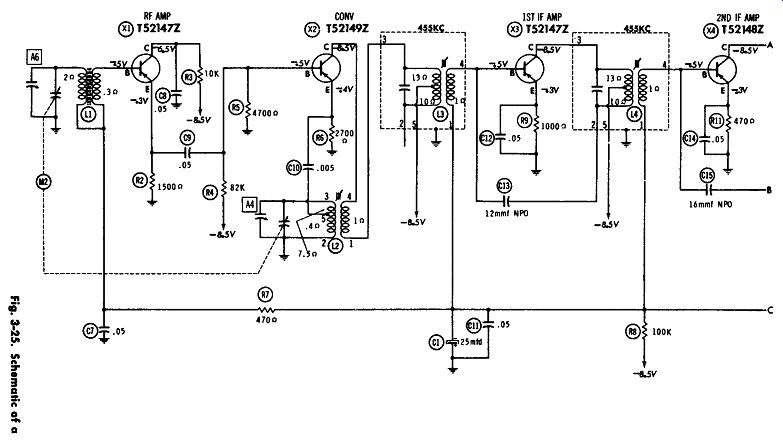
Fig. 25
Fig. 25 shows the complete schematic of this eight-transistor radio.
L1 is an antenna transformer wound on a metallic rod; it receives the incoming signal. The tank circuit, composed of coil L1 and one section of capacitor M2, is tuned to the carrier frequency. Transistor X1 is an RF amplifier operated in an emitter-follower configuration.
It provides an impedance match between the antenna and the converter stage. The collector of this stage is effectively signal-grounded by the bypass capacitor ( C8). Resistor R3 is used as a decoupling resistor.
It is also used to establish the proper voltage at the collector of transistor X1.
The RF signal is coupled to the base of the converter through coupling capacitor C9. Transistor X2 is used as an oscillator, mixer, and converter. The oscillator coil (L2) is comprised of two windings, the primary connected in series with the collector and the secondary tuned by one section of capacitor M2. The feedback signal from a tap on the tuned secondary is applied at the emitter of transistor X2. The frequency of the oscillator is maintained at 455 khz above the desired signal, and this provides an intermediate frequency of 455 khz in the collector circuit. The IF transformer ( L3) in the collector of the connecter stage is tuned to accept a 455- khz signal, and it rejects all other frequencies. The secondary of this transformer (L3) applies the signal to the base of transistor X3.
The second and third IF stages in this receiver are neutralized. This is accomplished by a signal that is fed back to the base of the transistor by neutralizing capacitors C13 and C15. To prevent oscillation of the stage, the feedback signal must be of the proper phase. For this reason the values of C13 and C15 are critical.
Negative bias for the RF, first IF, and second IF stages is obtained through the 100K resistor ( R8). A biasing divider network is composed of resistors R8 and R10 and volume control R1. This network is also part of the automatic gain control (AGC) system.
The signal applied to the detector diode produces a positive voltage across RF filter capacitor C1 6. This positive voltage is added to the negative voltage at the volume control, thus reducing the bias on the AGC line. Resistor R10 is placed in series with the volume control and the AGC filters (C1 and C11) to isolate the audio from the AGC line.
The audio signal is coupled from the center tap of the volume control to the base of the audio amplifier by electrolytic capacitor C2. Because of the low impedance of transistor circuits, it is necessary to use high value capacitors to obtain low-frequency response. Since electrolytics are used for coupling, it is important to observe the polarity of the coupling capacitor when it is being replaced.
The output of the audio amplifier (X5) is applied to the driver transistor (X6). This stage is a second audio amplifier and is called a driver. Unlike the vacuum tube, the transistor requires both voltage and current input in order to function properly. The purpose of a driver is to provide the correct amount of voltage and current drive to the output transistors. Driver transformer T1 has two secondary windings to provide a push-pull signal to drive the output transistors (X7 and X8). The speaker in this receiver is coupled to the output transistors by the 100-mfd capacitor (CS). This capacitor is used to block the DC from the voice coil. Tone compensation for the receiver is provided by a feedback network from the speaker to the emitter of the driver transistor. Also, to prevent an excessive rise in the impedance of the output transformer, capacitor C18 is placed across the transformer primary.
AUDIO AMPLIFIER
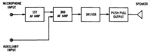
Fig. 26. Block diagram of an audio amplifier.
Another typical use of transistors is in audio amplifiers. Fig. 26 shows a block diagram for a Bogen public-address type amplifier that operates as a mobile unit from either a 6 or 12V power supply. It has facilities for two inputs--one for a microphone and one for an auxiliary input, such as a record player, radio, etc. Since the output level of a microphone is low, an extra stage of amplification is required. The auxiliary input is connected to the second amplifier. The output of the second audio amplifier feeds an audio stage that drives the push-pull output stage. An audio frequency amplifier must be able to amplify the entire audio spectrum from approximately 100 hz to 15 khz.
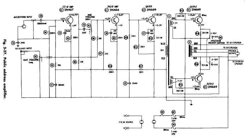
Fig. 27
Fig. 27 shows the schematic for this AF amplifier. The microphone input is capacity-coupled by C8 to the base of transistor X 1. The first stage transistor (X1) is used as a preamplifier for the microphone.
Bias for X1 is obtained from the power supply through the voltage divider composed of resistors R3 and R4. R1 is the volume control for the microphone (MIC) input. It is also used as part of the biasing network for transistor X2. Bias for the driver transistor (X3) is obtained directly from the collector of the first audio stage. The signal is direct-coupled from the second audio stage to the driver. The output of transistor X2 is direct-coupled to driver transistor X3. This stage feeds the driver transformer (T1) which, in turn, feeds the push-pull output transistors (X4 and X5). T2 is an impedance-matching trans former that enables the amplifier to drive a 16, 8, 4, or 2-ohm speaker by merely changing the connections.
This audio amplifier may be used with either of two supply voltages-a 6V battery or a 12V battery. When used with a 6V battery, resistors R14 and R16 are shorted. When used with a 12V battery, resistors R 15 and R 14 are used to stabilize the output transistors against thermal runaway.
REGULATED POWER SUPPLY
An unregulated power supply has a significant disadvantage in that the output voltage does not remain constant under varying load conditions. For example, if the open circuit voltage of a DC power supply is 20V and the application of a 2,000-ohm load resistor causes the output voltage to drop to 14V, the power supply is just not large enough to supply all the necessary current. There are many types of circuits which will not operate properly unless the supply voltage remains absolutely constant as the load changes. Transistors can be used to "regulate" power supplies so that the output voltage remains constant.
It was shown in Section 2 how a zener, or breakdown, diode may be used to regulate the output voltage of a power supply. Although the use of a zener diode is certainly an improvement, the regulation can be still further improved by the use of a transistor voltage regulator.
Fig. 28 shows a schematic diagram of a basic transistor voltage regulator. The circuit function of X1 is to control the voltage drop across the output. A sensing circuit is used to measure the output voltage. If the output voltage should begin to drop, a signal is fed to the series regulator, reducing its resistance and allowing more voltage to be applied to the load, thus bringing the output voltage back to normal. Should the output voltage tend to rise, a signal is fed to the series regulator, causing its resistance to increase and thus reducing the voltage applied to the load. The net effect is to maintain the load voltage at a constant level under varying load conditions.
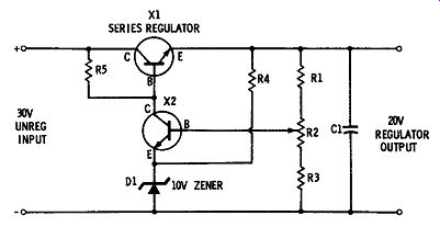
Fig. 28. Voltage regulator.
D1 is a zener connected in series with R4 across the output of the supply. The voltage across the zener diode is always at a constant value-in this case 10V. This constant value provides a reference voltage with which to compare the measured output voltage. The voltage divider made up of R 1, R2, and R3 provides a voltage of approximately 10V that is fed into the base of transistor X2. The difference between this voltage and the zener reference voltage will determine the bias on transistor X2. R2 is a potentiometer which is used to adjust the bias on transistor X2. Resistor RS is the load resistor for X2. The junction of this resistor and the collector of X2 is directly connected to the base of series regulator X1.
If the output voltage tends to drop, the bias on X2 decreases, reducing its conduction and increasing the voltage at the base of the current regulator. An increase in current through the series regulator returns the output voltage to the original value. If the output voltage increases, the bias on X2 increases, causing a decrease in the bias current applied to X1. A decreased current flow in the series regulator reduces the voltage to the original value.
This is a simple form of transistor regulated power supply. More complicated systems can be designed, but each is based on the principles described. The output voltage is sampled and the result is used to influence the amount of voltage applied to the load. A series regulator may be considered as a valve that is opened or closed, depending on how much voltage or current is needed for the load.
HEAT SINKS
It has been said a number of times in this guide that the main disadvantage of transistors is their sensitivity to heat and temperature. If the heat generated by conducting transistors is not dissipated in some manner, it can result in the destruction of the semiconductors or other components. As a result, many devices are used to remove the heat from the vicinity of the transistors. These include fans, blowers, heat sinks, etc.
A heat sink is a piece of metal that is used to conduct the heat-away from the circuit. Some heat sinks are finned for more efficient cooling.

Fig. 29. Finned heat sink.
In other applications the chassis can be used as a heat sink, particularly when the transistor is mounted in direct contact with it. Fig. 29 shows a power transistor mounted on a typical finned heat sink. Heat sinks are generally used with power transistors, rectifiers, series regulators, or other semiconductors that are conducting large amounts of current.