AMAZON multi-meters discounts AMAZON oscilloscope discounts
Until now, as far as linear active semiconductors are concerned we have discussed
only transistors. There are other solid-state devices, however, such as tunnel
diodes, photocells, and field-effect transistors; their operation is based
on the material discussed in Section 1. This section is concerned with a few
of these devices and some of the more common circuits in which they are used.
FIELD-EFFECT TRANSISTORS
Sometimes it seems as though field-effect transistors ( FET) should have been discovered before ordinary transistors. The reason for this is that their operation is very similar to that of vacuum tubes. The FET comprises a bar of semiconductor material through which current flows, while the resistance of the bar is controlled by the application of a field. It is quite similar to a vacuum tube, where the resistance between plate and cathode is controlled by the voltage on the grid. A field is used to control the resistance in the semiconductor, thereby curtailing the flow of majority carriers--thus the name field-effect transistor.
You will recall that a transistor is a minority-carrier device in which minority carriers are injected into the base and are conducted to the collector. A field-effect device is a majority-carrier semiconductor. The semiconductor bar, whether P or N, is doped to provide majority carriers. These carriers flow through the material, never crossing a PN junction. The resistance of the material is controlled by applying a field; Fig. 1 shows the functional diagram of a field-effect transistor.

Fig. 1. N-type field-effect transistor.
The left side of the main block of the silicon is considered the source of current, and the right side (called the drain) is the side from which the current leaves the device. The gate is the area which controls the resistance of the bar. If the bar is N-type material, the gate is made from P-type material. It is diffused into the bar by one of the methods described in Section 3. The PN junction at the gate is reverse-biased, and current carriers are removed from the vicinity of the gate. This sets up a space charge that makes it difficult for carriers to get through.

Fig. 2. Schematic of N- and P-type field-effect transistors.
Another way to look at it is that the resistance of the bar is increased by removal of the majority carriers. The more reverse voltage applied to the gate, the greater the space charge becomes and the more difficult it is for electrons to get from the source to the drain. The point at which the field becomes great enough to prevent electrons from passing the gate is referred to as pinch off. The reverse voltage that causes this is called the pinch-off voltage. Fig. 2 shows the approximate mechanical configuration and the schematic for N- and P-type FET's. Note that there is no such thing as a PNP or NPN FET. They are either N or P types, depending on the bar material. Fig. 3 shows the analogy between the FET and the vacuum tube. The source can be likened to the cathode, the drain performs the same function as the plate, and the gate acts the same as the grid. Circuits using an N-type FET are very similar to vacuum-tube circuits.

Fig. 3. Comparison between a vacuum tube and an FET.
As a matter of fact, the field-effect transistor and the vacuum tube are so much alike that one can use the terminology almost inter changeably and the design methods are almost identical. Bias for the FET is supplied in the same manner as it is for the vacuum tube. The input resistance of an FET is very high. The gate-circuit junction is reverse-biased and no current flows; thus the input resistance is very high. A vacuum tube also has a very high input resistance. A transistor has a very low input resistance, because its input circuit is a forward biased emitter junction. Field-effect transistors will certainly appeal to anyone who is familiar with vacuum-tube circuits because the circuitry is almost identical. If a P-type FET is used, the polarities of the applied voltages are reversed.
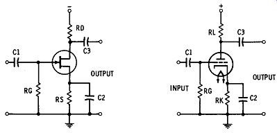
Fig. 4. Comparing an FET amplifier and a vacuum-tube amplifier.
Fig. 4 shows the similarity between a simple FET amplifier and a vacuum-tube amplifier. The FET is self-biased by the voltage drop across R,i, This makes the source positive with respect to the gate.
The vacuum tube is self-biased in a similar fashion by RK. R,, in the FET circuit stabilizes the bias by providing a return to ground for the small gate currents that exist. Ro; of the tube circuit performs the same function for the grid currents of a vacuum tube. C2 is an AC bypass capacitor that keeps the load current from influencing the bias.
It is significant to remember that in transistors the current carriers flow through the three different types of semiconductor materials that make up the base, emitter, and collector. In an FET, the current travels through only one kind of semiconductor from the source to the drain.
The resistance of the path can be varied by the voltage applied to the gate. Transistors create noise which is caused as holes and electrons combine.
The frequency response of transistors is limited by minority-carrier transient time. The current in an FET is a stream of electrons or carriers, the density of which is controlled by the gate. When the gate causes the resistance of the FET to increase, the current in the entire circuit changes and not just the current in the semiconductor. An FET does, however, have other problems that a transistor does not have.
One problem is that a large value of input capacity tends to limit the frequency response.
These FET devices are rather new and still mostly in the pilot production stages. In the months and years to come, construction techniques will undoubtedly be developed to overcome this input capacity problem. The main applications at the present time for field effect transistors are for semiconductor circuits having a high input impedance. In addition, the FET is capable of power gains far in excess of the ordinary transistor.
TUNNEL DIODES
Another interesting semiconductor device is the tunnel diode. It is sometimes referred to as the "Esaki" diode because it was discovered in 1958 by the Japanese scientist Leo Esaki. The Esaki diode may be used as either a linear amplifier or a nonlinear switching device.
A tunnel diode does not differ in physical construction from an ordinary diode, except that it is more heavily doped than the ordinary P-N junction. As a matter of fact, this is where the tunnel diode gets its name; it is so heavily doped that there are many millions of majority carriers crowded into the vicinity of the junction. A number of these majority carriers "tunnel" through the barrier that exists at the junction if a slight bias potential is applied. If the barrier is considered a potential hill, then the carriers can be thought of as having burrowed through the hill rather than going over it. Actually, tunneling takes place in a normally doped diode, but so few carriers are involved that the effect is not noticeable. It is only when the semiconductor is heavily doped, providing many majority carriers, that the tunneling effect becomes marked.
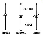
Fig. 5. Comparison of schematic symbols for the normal diode, tunnel diode,
and the zener diode.
Fig. 5 shows the schematic symbol for a tunnel diode. Symbols for the standard PN diode and the zener diode are shown for comparison. Tunnel diodes do not constitute serious competition for transistors as amplifiers in the lower frequency ranges because they do not provide as much gain as transistors in this area. But at the higher frequencies (microwave frequencies) above those at which transistors operate, tunnel diodes will function with sufficient gain to make them of great value.
Tunnel diodes may be used as amplifiers by virtue of the negative resistance portion of their characteristic curve. Before explaining what a negative-resistance amplifier is, let us first show how a tunnel diode exhibits a negative-resistance characteristic. Fig. 6 shows a tunnel diode characteristic and a normal diode characteristic. Note that the tunnel diode (Fig. 6A) conducts in the reverse direction, whereas the regular diode (Fig. 6B) does not. This is due to the fact that there are so many current carriers in the tunnel diode that they can conduct in either direction. Region I shows the application of a small forward bias (but not enough to overcome the barrier at the junction), resulting in a high forward conduction of the diode. This is due to the many majority carriers tunneling through the potential hill rather than going ...
( A) Tunnel diode (B) Regular diode
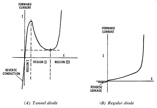
Fig. 6. Characteristic curves.
... over it. As the forward bias is increased ( Region II), the conduction begins to decrease and the diode curve is returned to the normal operating characteristic. Further increase in the forward bias results in Region III, which is normal diode behavior and corresponds to the diode curve shown in Fig. 6B. Region II is known as the negative-resistance portion of the tunnel diode characteristic. It is so called because an increase in voltage results in a decrease in current. A normal positive resistance will behave in just the opposite fashion: an increase in voltage will cause an increase in current. This interesting characteristic of tunnel diodes can be used for many things, among which is the linear amplifier. In order to be used as a linear amplifier, the negative-resistance portion of the curve can also be used to make tunnel-diode oscillators and mixers.

Fig. 7. Tunnel-diode curve.
The negative resistance referred to is not actually a minus resistance; it is a function of change in voltage across the diode as related to the change in current through the diode. On the tunnel-diode curve in Fig. 7, points A and B indicate a change in voltage of 10 millivolts and a current change of 0.7 milliamp. Note, however, that while the voltage is increasing (going in a positive direction), the current is decreasing ( going in a negative direction). The formula for AC resistance can be derived from this relation. It is equal to the change in voltage divided by the change in current.
The AC resistance of a minus 13.3 ohms represents a dynamic characteristic of the tunnel diode, whereas the actual DC resistance of the tunnel diode at point A or B is a positive resistance. This DC resistance can be calculated by dividing the positive voltage by the positive current.
The negative-resistance portion of the tunnel-diode curve can be used to amplify a signal. Fig. 8 shows a typical tunnel-diode amplifier complete with biasing circuitry. Bias current is supplied by A through the 2K resistor. R1 (150) is the load resistor. This circuit is shown merely as an example and would not really be practical, except at very high frequencies ( for example, 100 mhz). The negative-resistance portion of the tunnel-diode curve may be used in the construction of oscillators, pulse circuits, and other devices. Usually tunnel diodes are not used unless frequency or size limitations necessitate their use.
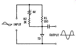
Fig. 8. Tunnel-diode amplifier.
HALL EFFECT
The Hall effect was discovered by E. H. Hall in 1879 at Johns Hopkins University. However, there was no practical use for the device because the output voltages available from materials at that time were very small. It was not until the advent of modern semiconductors that the Hall element became a circuit practicality. The successful operation of a Hall device depends on a semiconductor material with a large number of available current carriers. The material used is either P or N, and there are no junctions with which to be concerned.
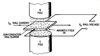
Fig. 9. Basic Hall effect.
Fig. 9 shows the basic Hall effect. If a semiconductor, such as germanium, is subjected to a magnetic field that is perpendicular to current flowing through the element, a voltage will be produced across the element. This voltage is proportional to the product of the current and the field ( current x field). The Hall element can be used for many applications. For instance, it is widely used in measuring magnetic field intensity. It can be used to measure current, as a proximity...

Fig. 10. Physical configurations for commercial types of Hall-effect devices.
...detector and as a multiplier. Fig. 10 shows the physical configurations for commercial Hall-effect devices. There are four output leads-two for current and two for voltage. The same two devices are shown in Fig. 11 to demonstrate the relative physical size of the Hall-effect devices.
A simple system for measuring magnetic-flux density around a magnet is to use a Hall-effect device mounted in a probe. The current through the Hall device is maintained at a constant level, and the output voltages will then be proportional to the magnetic-field strength.
The Hall voltage is amplified and indicated on a meter. By taking readings from the meter with the probe at different points, it is possible to plot the field around the magnet.
It is also possible to tell how far a Hall-effect device is from a magnet with a given field strength. This is determined by the magnitude of the voltage that is generated. Used in this fashion, it is known as a proximity, or nearness, detector. It can also be used to indicate angular position when used with two magnets. The Hall voltage will be greatest when the element is parallel to the faces of the two magnets. As the element turns, the output voltage will become less. Thus, the output voltage depends on the angular position of the Hall element.
PHOTOTRANSISTORS
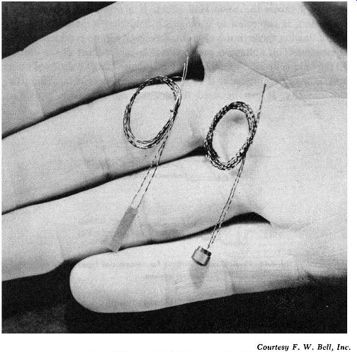
Fig. 11. Hall-effect devices of fig. 10.

Fig. 10. Courtesy F. W. Bell, Inc.
In Section 2 we discussed photosensitive diodes. The same principle may be applied to transistors. The three-element device is mounted in a standard transistor case with a lens at the top. When light is focused on the emitter junction, the transistor behaves like a photo diode, and the photoelectric action is amplified by the gain of the transistor. This often eliminates the need for a succeeding amplifier stage that is usually necessary when a photodiode is used. Fig. 12 shows the basic physical construction of a phototransistor and the schematic representation for the PNP and NPN types. The arrows in the schematic represent the incident light.
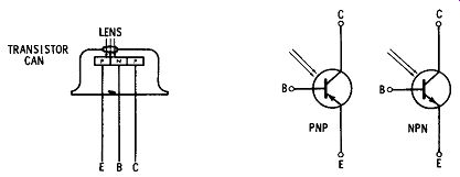
Fig. 12. Phototransistor.
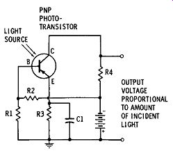
Fig. 13. Light level indicator using a phototransistor.
Phototransistors are used in a wide variety of applications. They are fairly linear and can be used to measure light intensity when used in a circuit like the one shown in Fig. 13. This circuit has disadvantages, however, which usually result in the use of some other means of measuring light intensity. The main disadvantage is that phototransistors operate over a very limited light range. In other words, it doesn't take much light to saturate the transistor. Usually density filters, or graded apertures, are used to extend the range of these devices when a wide range of light intensity must be measured.
Photodiodes, as well as phototransistors, are generally used in switching nonlinear or on-off applications.