AMAZON multi-meters discounts AMAZON oscilloscope discounts
We are all familiar with the standard transistor package and have to admit
that, compared to vacuum tubes, transistors are quite small.
The discovery of transistors has brought startling reductions in the size of electronic equipment: radios are truly vest-pocket size, hearing aids are now so small that "even your friends won't know," and television receivers are actually portable. And yet, if we take a close look at the cutaway sketches of transistor envelopes in Section 3, we will conclude that in the tiny transistor envelope the greatest percentage of the space is wasted. The actual transistor occupies only a small fraction of the available room. The only factor determining the size of the transistor is the method by which it will be handled. People and machines have to be able to pick it up, attach leads to it and place it into a circuit. With modern techniques steadily improving, the smallest possible transistor gets smaller every day.
Courtesy Fairchild Semiconductor
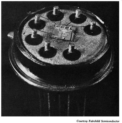
Fig. 1. Microcircuit attached to a lead header.
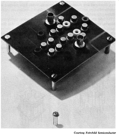
Fig. 2. Microcircuit shown beside the conventional circuit it replaces.
Courtesy Fairchild Semiconductor
Integrated circuit techniques enable dozens and even scores of components to be mounted in the space ordinarily occupied by a single transistor. This means that entire circuits can be placed on a semiconductor chip hardly big enough to pick up. The word "integrated" is derived from the fact that all the components, transistors, resistors, and capacitors are fashioned from semiconductor material.
There are no discrete components; that is, there are no resistors or capacitors that can be put in or taken out of the circuit. They are all integrated into one circuit function. There are no solder joints, and the only connections involved are those leads which connect the integrated circuit to the associated circuits. Fig. 1 is a photograph of a typical microcircuit mounted on a seven-lead transistor-type header. The top of the can has been cut away.
As in the case of putting many vacuum tubes into one envelope, it would seem that a respectable goal would be to put more than one transistor in a can. The transistor manufacturers went one better; they put complete circuits and even groups of circuits in the space previously reserved for one transistor. As a matter of fact, as many as 15 or 20 transistors and all the associated resistors and capacitors can be put onto a semiconductor chip measuring a few square millimeters.
And to add to what already seems to be a remarkable achievement, these integrated circuits are far more reliable than the corresponding circuit built from standard components and, in most cases, they are less costly! Fig. 2 demonstrates one example of the circuitry that can be packaged in a single unit. The solid-state circuit in the upper portion of Fig. 2 is replaced by the microcircuit shown below it.
The saving of size alone would not justify these small packaging concepts if cost and reliability had to be sacrificed. Consider the fact that microcircuits are basically more reliable than standard circuitry, the number of solder connections and welds are reduced, and the resulting circuit is much more reliable. The techniques which have been developed and mastered by the manufacturers have resulted in mass-production methods which turn out circuits economically competitive with standard discrete component circuits.
The fully integrated circuit is one where the components, transistors, resistors, and capacitors are all made from semiconductor or thin film materials inseparably associated with each other on a silicon wafer or chip. Unlike standard circuitry, it is impossible to remove a component from an integrated circuit. This, of course, means that defective units must be thrown away and replaced with a new one.
INTERCONNECTIONS
(A) Exploded view (8) Normal.

Fig. 3. Cordwood module.
A number of microelectronic approaches preceded the fully integrated circuit. The great-grandfather of the integrated circuit involves high-density packaging using discrete components. This generally takes the form of what is known as the "cordwood" approach to packaging.
Fig. 3 shows a sketch of a cordwood module. It uses standard components placed as close together as possible. It gets its name from the fact that the components are stacked the same as cordwood. The cordwood method is still in wide use and for many applications it is the best package.
The next advance was to use uncased transistors, or transistor "chips" as they are called. This substantially reduced the package size by eliminating the "wasted" space inside the transistor can.
The next step closer to fully integrated circuits is the hybrid circuit,...
Courtesy Lockheed Missiles and Space Co.
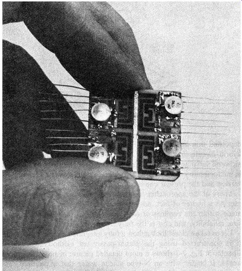
Fig. 4. Titanium thin-film circuits on a single substrate.
...such as the one show in Fig. 4. These use discrete active components (transistors) and thin-film passive components. Thin metallic films are deposited on a substrate, usually some kind of ceramic, to make up resistors and capacitors. The active components are then mounted on the substrate to complete the module. Resistors are made by con trolling the shape and resistance of the metallic film. Capacitors are formed by placing a nonconductive dielectric between two layers of

Fig. 5. Hybrid thin-film circuits.

Fig. 6. Size reduction of an amplifier.
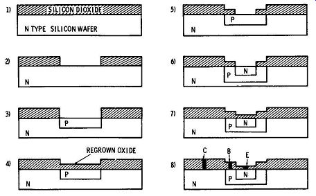
Fig. 7. Planar-passivated process.
deposited thin metallic films. Fig. 5 shows how the basic thin-film hybrid circuits are fabricated. Fig. 6 shows how the size of an airborne servo amplifier has been reduced over the years by advances in microcircuitry techniques. The original amplifier was a vacuum tube version and the present one is a thin-film hybrid.
Many of the approaches to microelectronics are still very much in use. As a matter of fact, advancements and improvements are being made within the confines of each concept, but the ultimate in small size, reliability, and cost is the fully integrated circuit.
Let us take a closer look at how a fully integrated circuit is processed.
It is constructed using the planar-passivated method described in Section 3. Fig. 7 shows a more detailed picture of how this process works. It begins with an N-type silicon wafer that is oxidized. The impurity material will not diffuse into the passivated layer and therefore the oxide is first etched away over the area where the diffusion is to take place. A PN junction is then diffused into the wafer and another layer of oxide is grown. A certain portion of this is in turn etched away to prepare for the next diffusion. After the complete NPN transistor has been constructed, the base, emitter, and collector contacts are metallized and leads are attached.

Fig. 8. Mass-produced microcircuits.
The method of etching away the oxide at those places where you wish to put the next diffused junction is done by a photographic process.
The oxide-coated surface is covered with a chemical that hardens when exposed to light. A mask is placed over the surface to block out the portions where the next diffusion is to take place. After exposure to light, the chemical under the masked part of the surface does not become hard and it washes off. The wafer is then placed in another chemical which etches away only the exposed oxide. It is then placed in the diffusion ovens and the new junction formed. This process can be repeated as many times as desired. The junctions can be made as small as it is possible to make the photographic masks. In actual practice, hundreds of junctions can be formed simultaneously. Fig. 8 shows a mass-produced wafer containing more than 400 individual circuits. After completion, the larger wafers are then cut up or "diced" into individual circuits, leads are attached, and the microcircuits are then mounted for convenient use.
The basic wafer on which the integrated circuit is built is called a substrate. Fig. 9 shows five diodes built into a common substrate.
This is a very simple circuit and would require only one diffusion.

Fig. 9. Integrated circuit containing five diodes.

Fig. 10. Transistor-diode gate.
Thus, all of the diodes necessary for five inputs to an AND or OR gate are contained in a very small space with no interconnecting wires to bother with, and at a competitive price. Fig. 10 illustrates how these five diodes can be built into the output of a transistor circuit all on the same substrate. This is a slightly more complicated integrated circuit and would require two diffusings. The light lines seen on the top of the crystal, around the transistor junctions, are oxide growth marks where the thickness of the oxide changes due to the etching and re-growing. The collector of the transistor and the cathodes of the diodes are common to each other, being formed out of the same piece of semiconductor. The base of the transistor and all the diode anodes would be formed by the first diffusion. The emitter of the transistor is a second diffusion. The aluminum contacts are made by evaporating aluminum onto the surface of the wafer through a thin metallic shadow-mask. Holes are punched in the mask at the places where the aluminum is desired. Leads are connected to these areas.
Fig. 11 A). In this circuit two
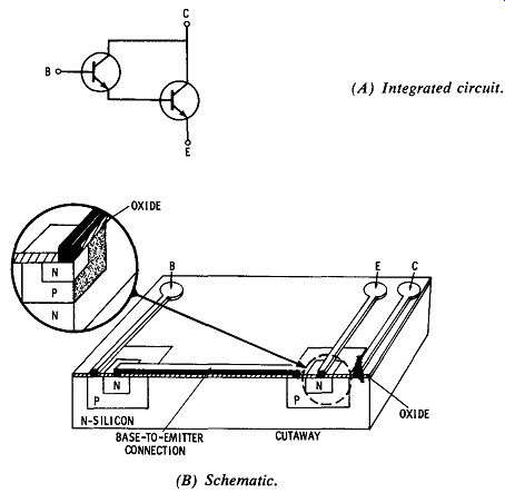
Fig. 11. Darlington amplifier.
(A) Integrated circuit.
(B) Schematic.
The simplest example of two transistors in one integrated circuit is that of the Darlington amplifier transistors are direct-coupled to provide increased gain. If the transistors in a Darlington pair had a gain of 100 each, the total gain of the circuit would be 10,000. Thus, you can see the possible applications of such a circuit. Fig. 1 1B shows the integrated circuit layout for a Darlington amplifier. The substrate is N-type silicon, which forms the collectors of both transistors. Then, by appropriate maskings, etchings, and diffusions the bases and emitters are formed. It is necessary to connect the emitter of one transistor to the base of the other. This is done with an aluminum conductor evaporated onto the surface. This aluminum conductor is deposited at the same time as the metalizing contacts. A double-cut view through the emitter connector is shown to illustrate how contact is made to the emitter and not to the base.
The oxide serves as the insulator.
(A.) Common collectors. ( B) Isolated collectors.
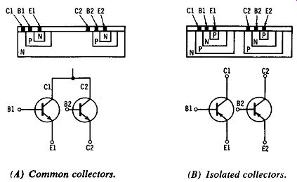
Fig. 12. Two transistors on one substrate.
The collector of a transistor must carry the maximum current in the device and, therefore, must be capable of dissipating the most heat. For this reason, the collector of an integrated transistor is always the substrate. The obvious question then becomes, how can two or more transistors be put on one substrate without having their collectors connected. A circuit containing two transistors with common collectors is shown in Fig. 12A. Fig. 12B shows a configuration with two isolated transistors. Notice that another junction has been added.
(A) Two transistors with common collectors. (B) Two isolated transistors. (C) Darlington pair.
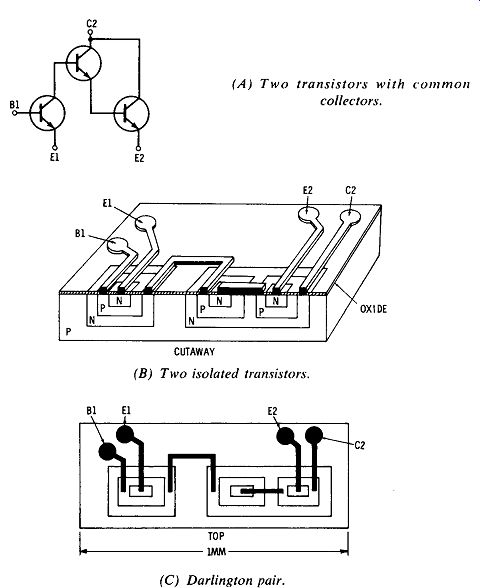
fig. 13. Three transistors on one substrate.
This junction is then reverse-biased to prevent current flow between collector 1 and collector 2. Fig. 13A shows a circuit containing a Darlington amplifier and a driving transistor. In Fig. 13B note that the collector of the first transistor is isolated from the collectors of the Darlington pair by the reverse-biased isolation junctions. Notice that the top view (Fig. 13C) shows the transistor as three concentric squares. This is a good way to pick out the transistors on a micro photograph of an integrated circuit. They are not always squares, but three shapes ( one inside the other) usually indicate a transistor.
(A) A grid between transistors.
(B) Multiple grids.
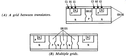
Fig. 14. Grid isolation.
Another method of isolating adjacent transistors from each other involves diffusing a junction completely through the basic wafer (Fig. 14A). This provides two reverse-biased junctions, called a grid, between the transistors. The effective amount of isolation can be increased by increasing the number of grids, as in Fig. 14B. The main disadvantages of this method are that long diffusion times are required and maskings must be performed on both sides of the wafer.
Both of these isolation methods have advantages for certain applications, and they are used in circuits.
Now that we can put as many transistors on a substrate as we wish, let us discuss methods for integrating other components, such as resistors and capacitors. Resistors are fairly easy to make since a semi conductor is a resistor whose resistance depends on the amount of doping. In addition, the length, height, and width of the resistive path will determine the resistance. If a certain length of semiconductor has a resistance of, say, 50,000 ohms, it will have twice as much resistance if the path for current carriers is cut in half and four times the resistance if the path is divided by four. Thus, different thicknesses and lengths of doped semiconductor may be used to provide different resistances.
(A) Single resistor. (B) Tapped resistor.

Fig. 15. Integrated resistors.
(A) Schematic
(B) Integrated circuit
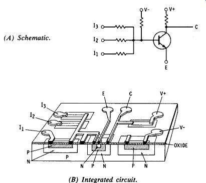
Fig. 16. NOR gate.
There are two basic methods of using this principle to form resistors in integrated circuits. One method uses the semiconductor material itself, while the other involves depositing resistive elements on the surface of the wafer very similar to the thin-film resistors described earlier. In the case of the former (Fig. 15A) a channel is cut through the oxide and contact is made at the ends of a previously formed resistor strip. The resistance depends on the length, width, depth, and doping level of the strip. Fig. 15B shows how the addition of a conductor forms a resistor voltage divider. The ratio of the two resistances will be determined by the placement of the conductors.
The application of these principles is shown in Fig. 16. The circuit for a three-input NOR gate is shown in Fig. 16A, and Fig. 16B shows a cutaway of the integrated circuit. This particular circuit could easily be put onto a !-millimeter square. A number of such circuits can be mounted in a single transistor envelope.
Thin-film resistors can be deposited in the same manner as the metallized contacts (through a shadow-mask), but they are usually applied by photo methods. That is, the entire wafer is coated with the film and then the desired pattern is left after etching. These thin-film resistors are not semiconductors, but are made of metals such as nichrome, a mixture of nickel and chromium) and cermet (a mixture of ceramic and metal). In the case of thin-film resistors, there are no tell-tale oxide growth marks, but often they appear as thin lines running back and forth across the chip, as in the case of the hybrid circuits.
(A) Junction capacitors.
(B) Oxide capacitors.

Fig. 17. Integrated capacitors.
(A) Schematic. (B) Circuit on substrate.

Fig. 18. Typical integrated circuit.
There are two basic ways of making capacitors for integrated circuits.
The first utilizes the inherent capacity of a PN junction (Fig. 17 A). The second uses the silicon dioxide as a dielectric (Fig. 17B). The junction type has two main disadvantages: first, the capacitance value is sensitive to the voltage across the junction; and second, a PN junction will conduct in one direction and, therefore, the junction capacitors must be reverse-biased in order to operate. The oxide dielectric capacitor is more stable than the junction type, but only a few hundred picofarads of capacity can be formed by this method. A conductor is placed on top of the oxide layer and connection is made to the semiconductor under it. Thus the oxide acts as the dielectric for the capacitor.
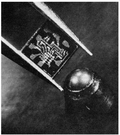
Fig. 19. Microphotograph of a microcircuit. Courtesy Fairchild Semiconductor.
Fig. 18B shows the layout of a typical integrated circuit containing two transistors, three resistors, and one capacitor. The schematic diagram of this circuit is shown in Fig. 18A. All the components are made by the photographic masking techniques mentioned earlier.
The components are electrically separated on a single substrate by isolation diffusion. The transistors are NPN types, the resistors are N-type semiconductor strips, and the capacitor is an oxide type. Fig. 19 is a microphotograph of an integrated circuit, showing the relative size compared to that of a ball-point pen.
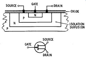
Fig. 20. Integrated field-effect transistor.
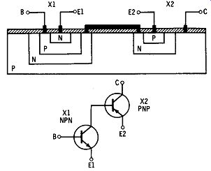
Fig. 21. Integrated circuit and schematic of complementary transistors.
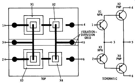
Fig. 22. Integrated differential amplifier and schematic diagram.
Another important semiconductor device which lends itself to easy integration is the field-effect transistor. Fig. 20 shows how this is accomplished. Recall that the source and the drain are connected to different ends of the same type of material. The gate is used to restrict the flow of current carriers from the source to the drain as a function of the voltage applied to the gate. The same isolation techniques are used for FET's as for regular transistors. The methods of constructing FET integrated circuits are completely compatible with those for normal transistors; thus, there is no problem in building both into the same circuit.
Another structure that lends itself to the use of integrated circuits, although it does not use devices or techniques other than those we have already mentioned, is the complementary circuit. This requires two complementary transistors ( an NPN and a PNP) in the same circuit. The collectors are direct-coupled to the bases of the opposite transistor type (Fig. 21). Three junctions are used to construct an isolated NPN transistor, and the basic P substrate is used as the collector of the PNP transistor. Fig. 22 shows the schematic and top view of an integrated circuit of a typical differential amplifier.
You are probably wondering why we have neglected to discuss integrated inductances. The reason is very simple-there is no good way to integrate inductance. For this reason, integrated circuits have found their best acceptance in the area of digital circuitry. Linear communications-type circuits require tuned circuits, and as yet there is no way to build an inductance out of semiconductor materials or junctions. A high-quality RF or IF stage cannot yet be made in integrated form. In addition to this, the tolerances of resistors and capacitors that must be lived with at the present are in many cases outside the realm of desirability for good linear amplifiers.