AMAZON multi-meters discounts AMAZON oscilloscope discounts
Research into the basic fundamentals of semiconductor theory has produced
a variety of devices, each of which performs a particular, specialized function.
Among these is the unijunction transistor that is used primarily as a pulse
generator, as well as the four-layer device used as a switch or controlled
rectifier.
UNI-JUNCTION TRANSISTOR
The unijunction transistor is so named because it has only one junction. Its operation differs considerably from that of the ordinary transistor. Fig. lA shows a pictorial diagram of a unijunction transistor. It consists of two bases and an emitter. The two bases are connected to a semiconductor bar of N-type silicon, and the emitter forms a P-N junction with the silicon. When the voltage applied across bases B1 and B2 is 20V and the emitter junction is located halfway between the two base contacts, the silicon bar will act as a voltage divider and+ 10V will exist at the emitter. The resistance between the emitter and B1 will be relatively high. In order to forward-bias the emitter junction, an input voltage of -10V must be applied between the emitter and base 1. When a voltage sufficient to overcome this reverse bias is applied to the emitter, the unijunction transistor fires and the resistance between the emitter and B 1 becomes very small.
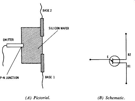
Fig. 1. Unijunction transistor. (A) Pictorial. (B) Schematic.
The best way to understand the operation of a unijunction transistor is to consider it in a simple application. Fig. 2 shows the unijunction transistor in a typical relaxation oscillator circuit. Assume that resistor
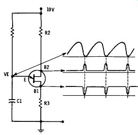
Fig. 2. Unijunction relaxation oscillator.
R1 and capacitor C1 are not in the circuit. A portion of the positive voltage will appear across the silicon bar, and the emitter junction will be reverse-biased. In order to overcome this reverse bias, it is necessary that the emitter become more positive than the N side of the P-N junction. R1 and C1 are used to produce this voltage. C1 will charge through R1 from the + 10V supply. When the voltage across C1 reaches a point where it forward-biases the emitter junction, the resistance of the bar from emitter to base 1 becomes very low and this circuit conducts heavily. Capacitor C1 discharges through the uni-junction and resistor R3, providing an output pulse across R3. When there is a positive pulse at B1, B2 will produce a negative pulse because the B1-B2 resistance is lowered, thus bringing B2 closer to ground.
After the discharge of capacitor C1, the voltage at the emitter is nearly zero, the junction is reverse-biased, and the process repeats. The wave shapes shown in Fig. 2 indicate how C1 charges through R1 until the unijunction fires and C1 discharges through R3. The frequency of the output pulses is determined by the values of resistor R1 and capacitor C1.
The unijunction is often used as a pulse generator in timing applications. Its main advantage over a transistor pulse generator is that it requires fewer components, as can be seen by comparing it with the circuit of a free-running multivibrator. In addition, it is easy to calculate the frequency of the output pulses from the RC time constant of R1 and C1. Uni-junctions are often used in the triggering and firing circuits of silicon-controlled rectifiers.
FOUR-LAYER DEVICES
Fig. 3 shows the pictorial schematic symbol for a P-N-P-N four layer device. Voltage drops across the junctions in Fig. 3A are caused by leakage currents that forward-bias junctions J1 and J3 and reverse bias junction J2. Until J2 becomes forward-biased, the device will present a very high resistance. When the voltage applied across the device becomes large enough, junction J2 breaks down and the device becomes a short circuit.
Fig. 3B shows the transistor equivalent to the four-layer device.
If enough forward voltage is applied from the emitter of the P-N-P to the emitter of the N-P-N, the transistor pair can be made to conduct...
(A) Description of structure. (B) Transistor equivalent of 4-layer device.

Fig. 3. 4-layer semiconductor device.
(A) Shockley, or 4-layer diode. ( B) Silicon controlled rectifier. (C) Complementary (D) Silicon SCR. controlled switch.
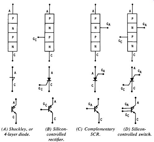
Fig. 4. Types of 4-layer devices.
...heavily. As mentioned, the natural voltage drop across the junctions causes J1 to be forward-biased along with J3. By increasing the voltage across the entire device, more electrons crowd into the P-side of the J2 region and more holes crowd into the N-side of J2, finally providing enough minority carriers to cause J2 to start conducting. At this point the device fires. Junction J2 becomes forward-biased because of heavy current carrier traffic and the device exhibits a very low resistance from anode to cathode. Once the device is conducting heavily it is necessary to reverse-bias J2 to turn it off. The most common way to turn off a four-layer semiconductor device is to remove the anode potential. It will, however, turn off if the current is allowed to drop below a certain minimum value.
Fig. 4 shows the possible terminal connections of four-layer P-N-P-N devices. The diagrams directly below the pictorials are the symbols generally used in schematic diagrams. The schematics at the bottom are those that are used to a lesser extent. As shown in Fig. 3, if a large enough voltage is applied from the anode to the cathode, the four-layer device may be made to short-circuit and conduct very heavily. It is possible to control the firing point more accurately and with more flexibility with a lead on one of the other layers. These are called gate leads. A lead can be put on the N-layer, the P-layer, or both. This accounts for all possible types. The gates enable the introduction of current carriers and thus give greater control over the point at which the device will fire.
The four-layer diode shown in Fig. 4A is sometimes referred to as a Shockley diode. It has no gate leads and is turned on when the applied voltage exceeds the breakover voltage; it is turned off when the supply voltage is removed.
Fig. 4B shows a diagram for a silicon controlled rectifier. This type of rectifier is nothing more than a four-layer diode with a gate lead connected to the second layer.
Fig. 4C shows what is called a complementary SCR. The gate is on an N-type material instead of a P-type material. This means that the opposite type of current carriers used for the gating functions.
The SCR is in wide use in a multitude of circuits. It is noted for its ability to handle large currents at relatively high voltages and is widely used in AC power circuits.
The device represented in Fig. 4D is a silicon-controlled switch ( SCS). It embodies all the advantages of the other three devices. By using or not using the gate leads it is possible to employ this device in place of any of the others. In addition, it has a certain flexibility that enables it to be used in unique circuits where others cannot be used.
The silicon-controlled rectifier is the solid-state counterpart of the thyratron vacuum tube. If you are familiar with the thyratron you will remember that it is a gas-filled tube across which a voltage is applied.
A firing voltage is then applied to the grid, causing the tube to conduct. During conduction, the voltage on the grid has little or no control over the current flowing through the tube. The SCR performs in the same way. A voltage is applied across the SCR and the voltage on the gate lead controls the point at which the SCR breaks down and starts conduction. When the SCR has started conduction, the voltage on the gate lead has no effect and the only way the device can be turned off is to remove the anode voltage to the SCR.
(A) Sawtooth generator. (B) Pulse amplifier.
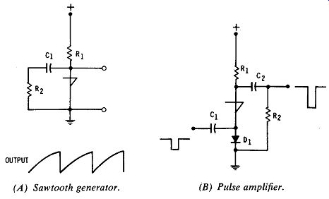
Fig. 5. 4-layer-cliode circuits.
Fig. 5 shows two typical circuits for a Shockley diode. The saw tooth generator of Fig. 5A operates very simply. C1 charges through R1 and R2 until the breakover voltage of the four-layer diode is exceeded. The device fires and C1 discharges; the diode shuts off and the process repeats. Fig. 5B shows a pulse amplifier. A negative input pulse causes the diode to fire and produce a high-power output pulse.
This type of circuit is often used for triggering squibs, an explosive charge used in missiles and rockets to separate unwanted parts. For example, on launch, the umbilical cord is blown away by a squib, and during flight, sections are separated by squibs.
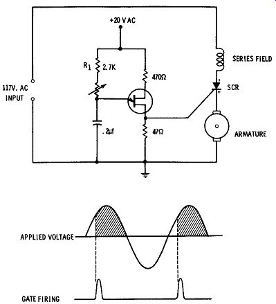
Fig. 6. Speed control for motor.
Fig. 6 shows a simple SCR circuit used for a motor speed control. This control is accomplished by varying the firing angle of the applied voltage with R1. Adjusting R1 changes the trigger point of the unijunction oscillator, and determines the point at which the SCR begins conduction and supplies voltage to the motor. The SCR can be made to fire at any point on the positive half cycle of input voltage.
Thus, the motor speed can be controlled over a given speed range by adjustment of R1. The negative half cycles serves to turn off the SCR until the next positive half cycle.
PHOTOTRANSISTOR USED AS A SWITCH

Fig. 7. Flasher using phototransistor.
Fig 7 shows a circuit for a simple light flasher employing a photo transistor. A phototransistor is equivalent to a normal transistor plus a photocell. In Fig. 7, when the lamp illuminates the phototransistor, it causes transistor X1 to become forward-biased and switch on. This pulls in the relay, opening the normally closed contacts. The lamp extinguishes, the photocell resistance increases, transistor X1 turns off, the relay drops out, and the lamp turns on to start the cycle again. R1 is the sensitivity control and capacitor C1 slows down the relay action so that the flasher frequency is not too high.
TUNNEL DIODE USED AS A SWITCH
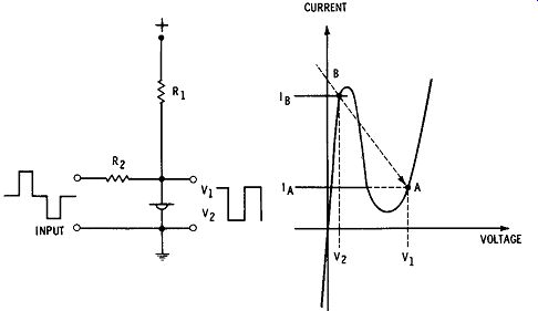
Fig. 8. Tunnel-diode circuit and characteristic curve.
In Section 4 it was mentioned that the best linear applications for tunnel diodes are at higher frequencies, where other components will not operate properly. This same idea holds true for tunnel-diode switching circuits. At present their main use is in high-frequency computer circuits.
Referring to Fig. 4-6, a tunnel diode may be made to switch from Region I to Region III and back to Region I again. Used this way it can perform the function of bistable and monostable circuits, as well as a square-wave multivibrator. Fig. 8 shows a simple tunnel-diode bistable circuit along with the characteristic curve to facilitate the explanation of switching. If the voltage and current are such that the diode operates at point A on the characteristic curve and a positive pulse is entered at the input, momentarily increasing the current and decreasing the voltage, the operating point on the curve will change to point B. Thus the trigger pulse switches the diode from one stable state to another. It can be switched back by a negative trigger pulse, causing the values to switch back to those represented by point A.