AMAZON multi-meters discounts AMAZON oscilloscope discounts
THE ZENER DIODE
The zener diode essentially is a silicon junction rectifier which exhibits abrupt conduction at a discrete reverse bias. Unlike semiconductor diodes used for rectification, wherein reverse conduction must be avoided, the zener diode is deliberately used in this operating mode. When so used, its effective DC resistance varies with the current, in a manner closely approaching the ideal characteristic of the shunt regulating element depicted earlier in Fig. 2-1A. Thus, the zener diode can provide a constant voltage to a load, in much the same way previously described for the gaseous tube.
There are numerous applications where high current capability takes precedence over extremely close regulation. This requirement is most simply and, often, most economically met by means of a shunt regulator employing a power zener diode. Also, back to back power zeners make satisfactory regulators for AC voltage in many cases. A considerable art has evolved about the zener diode, and, to thoroughly understand this fascinating device, one must become acquainted with the physics of semiconductors (which is outside the domain of this guide) . Rather, we shall be concerned only with the external characteristics of the device, and, in particular, with those related directly to its use as a shunt-type voltage regulator.
From the basic circuit in Fig. 3-1A you can obtain a better understanding of the operation of a zener diode. The characteristic curve of Fig. 3-1B is generally representative of any semiconductor rectifying diode. However, the relatively abrupt reverse conduction and nearly vertical slope of the curve in the reverse-conduction region are specifically characteristic of the zener diode. Disregarding the sign of the polarizing voltage and omitting the forward-conduction region, we can depict the curve as in Fig. 3-2. This clearly shows the similarity of the zener diode to the gaseous VR tube and thus enables us to visualize both devices as practical elements approximating the voltage-current relationship of the ideal element represented by the curve of Fig. 2-2D.
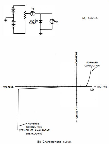
(A) Circuit. (B) Characteristic curve. Fig. 3-1 . General characteristics of
zener diodes.
Operating Voltages
Unlike with gaseous diodes, a wide selection of breakdown voltages-ranging between 3.9 and 200 volts--is available in zener diodes (see Table A-3 in the Appendix). As the semiconductor art progresses, even higher voltage units will probably become practical. The physics of the breakdown phenomenon is such that the closest approach to ideal shunt regulating characteristics is obtained for diodes designed for reverse-conduction voltages between 6% and 8% volts.
For this reason, it is sometimes desirable to employ series connected strings of such low-voltage units in order to achieve a higher breakdown voltage. Table A-3 shows Motorola power zener diodes in 10 watt and 50 watt capacities.
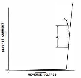
Fig. 3-2. Simplified method of depicting u the breakdown voltage characteristics
of the zener diode. REVERSE VOLTAGE
These have breakdown voltages ranging from 3.9 volts to 200 volts. In all instances, the diodes have reverse polarity when the letter R is appended to the type number. Reverse polarity corresponds to packaging in which the negative connecting terminal (anode ) is insulated from the stud or case. Such an expedient results in more precise DC regulation and lower dynamic output impedance than can be obtained from a single element rated at the higher voltage.
At the same time, such practice can entail greater expense.
In Fig. 3-3 we see a typical family of curves for zener diodes having various breakdown voltages. Keeping in mind that a vertical slope in the reverse-conduction region would provide perfect regulation and a zero dynamic output impedance (at least at low frequencies ), we can acquire a feeling for the relative "goodness" of such diodes in terms of their zener breakdown voltages. Inasmuch as zener diodes are employed most often in conjunction with transistors and other solid-state devices, it fortunately happens that breakdown voltages in the 6%- to 8%-volt region are practical for circuit operation. Notice that the curves for diodes B, C, and D of Fig. 3-3 are nearly vertical ; this signifies low dynamic impedance.
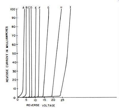
Fig. 3-3. General trend of reverse-conduction characteristics for zener
diodes with different breakdown voltages.
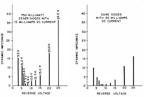
Fig. 3-4. Effect of operating current on dynamic impedance of various zener
diodes.
Table A-1 in the Appendix comprises a family of General Electric one-watt zener diodes. It is recommended that such one-watt units be substituted for their voltage counterparts in schematic diagrams calling for 200 mw, 400 mw, and 750 mw zener diodes. The use of one-watt units is advantageous for construction of experimental projects. The additional electrical ruggedness of these one-watt diodes provides increased protection against destruction with the often accompanying chain reaction burn-out of associated semiconductors. An additional bonus is obtained if the diode current is increased, for then a lower dynamic impedance results. The one-watt zener diode has been so reduced in price that initial selection cannot be rejected on cost alone.
Dynamic Impedance Effect of DC Current on Dynamic Impedance--In a given zener diode, the dynamic impedance decreases as the DC operating current rises. This is illustrated in Fig. 3-4, which shows the dynamic impedances of various diodes corresponding to two DC currents. Of course, the DC operating current cannot be increased without ultimately exceeding the permissible temperature rise of the junction. Inasmuch as the zener diode sometimes must dissipate considerable ripple power, the DC current alone may not constitute sufficient consideration in designing for safe operation. Safe operation may not actually be the limiting factor in deciding the maximum DC current to pass through a zener diode.
The temperature coefficient of zener diodes with breakdown voltages greater than about six volts becomes increasingly positive with more DC current. Unless compensating components with suitable negative temperature coefficients are present in the circuit, it may not be desirable to pass too high a DC current through a zener diode because the voltage breakdown could shift considerably with temperature variations. Aside from the effect of more or less DC current, conditions accounting for variations in the operating temperature of a zener diode are (1) an initial warm-up period, (2) proximity of heat-generating components, and (3) changes in the ambient temperature.
In order for manufacturers' values of dynamic impedance to be meaningful, it has become standard practice to designate the dynamic impedance of a zener diode for DC operating currents of 20 '1'0 of maximum permissible DC current at 25°C. Additionally, the measurement is carried out under the stipulation that the AC superimposed on the DC operating current is 10 % of that value and is a low-frequency sine wave, generally 60 hz. For example, a zener diode capable of withstanding a maximum DC current of 200 ma would be tested for dynamic impedance by superimposing 4 ma of 60-hz alternating current on 40 ma of DC operating current. The dynamic impedance would then be calculated by dividing by 4 ma the value of 60- hz voltage needed to produce the 4-ma AC current. If, in this particular example, 8 millivolts is required, the dynamic impedance of this zener diode would be quoted as .008 / .004, or 2 ohms.
Variations in Dynamic Impedance with Rated Power Dissipation--It has been shown that increased DC current in a given zener diode tends to lower the dynamic impedance.
Graphically, this is manifested by the fact that the characteristic curve is almost a vertical slope. If the DC current is made too high, however, excessive heat will be produced.
This results in an unstable coefficient of temperature with respect to voltage-that is, the breakdown voltage tends to lose even its short-term stability. A further increase in DC current will damage the junction. This behavior would, however, lead us to suspect that a zener diode with a junction having a large area-that is, one designed to carry more current-would have a lower dynamic impedance than a small diode. From a highly different viewpoint, we could liken a large-area junction to an equivalent parallel connection of an appropriate number of smaller junctions. Now we would expect the dynamic impedance of the large junction to be less than that of any smaller junction, because impedances in parallel result in a smaller net impedance than that of any of the constituents. As a matter of fact, zener diodes of high power rating do tend to have lower dynamic impedances than diodes with like breakdown voltages but smaller power or current ratings.
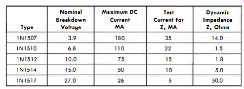
Table 3-1. Dynamic impedance versus power rating-typical 750-milliwatt zener
diodes

Table 3-2. Dynamic impedance versus power rating-typical 3.5-watt zener
diodes

Table 3-3. Dynamic impedance versus power rating-typical 10-watt zener diodes
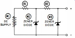
Fig. 3-5. Two-stage cascaded shunt regulator.
In Tables 3-1 , 3-2, and 3-3 we see a significant comparison of zener diodes belonging to three different families of power ratings. In all three, the maximum permissible current is the power rating divided by the breakdown voltage, and the DC test current for evaluation of dynamic impedance is approximately 20% of the maximum permissible DC current.
Dynamic Impedance and Series-Connected Diodes--Figs. 3-3 and 3-4 indicate that dynamic impedance tends to increase quite rapidly for diodes with breakdown voltages greater than 10 or 15 volts. Other things being equal, it is generally possible to obtain lower dynamic impedances by allowing more DC current to flow through a diode. This can even be exploited to the extent that a diode with a much larger power capacity is used than the demands of the external load would dictate. This is a practical technique for lowering the dynamic impedance for diodes with breakdown voltages higher than 20 volts or so, particularly when 50 to 100 or more volts must be stabilized. However, a better approach consists of connecting the appropriate number of low-voltage diodes in series. For example, three 8.4-volt diodes in series will result in an effective breakdown and stabilization voltage of about 25 volts. The dynamic impedance of the combination will be approximately the same as for a single diode, but the permissible power dissipation will be three times as much. Any number of low-impedance diodes can be series-connected to provide stabilization at a higher voltage.
Dynamic Impedance and Cascaded Shunt Regulators--The dynamic output impedance of a zener-diode voltage can also be lowered by cascading two or more stages. A two-stage arrangement is depicted in Fig. 3-5. The diode used in the first stage (M2) must have a higher breakdown voltage than the output stage. This arrangement significantly improves regulation with respect to the line or input voltage.
Stabilization of Small Voltages
Below 3.5 volts, the characteristics of zener diodes deteriorate to such an extent that these units are not generally available commercially. Even between 3.5 and 4 volts, the onset of conduction is "soft" ; and to attain a low dynamic impedance, such diodes must be operated with appreciable current. This is undesirable, for as we shall see, the already excessive temperature drift of low-voltage diodes is further degraded by the high current.
A very effective way of obtaining low-voltage stabilization is by means of the parallel network shown in Fig. 3-6. The output voltage is the difference between the breakdown voltage of the two diodes. Inasmuch as the two diodes will be similar, they may be expected to have fairly closely matched temperature drift characteristics. The output voltage will then be relatively immune to temperature, because the fact that the two diodes change in the same direction tends to maintain the same difference voltage. As an example, if 8.4- and 7.2-volt diodes are used, a stabilized output of 1.2 volts will be provided.
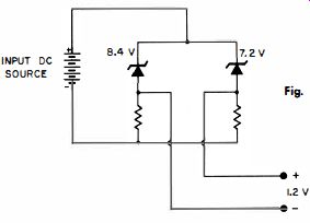
Fig. 3-6. Parallel network for obtaining low-voltage stability.
Temperature Coefficient
The zener breakdown voltage tends to be temperature-dependent. For many applications, the displacement of voltage with respect to temperature is too small to prove troublesome. It is fortunate that, generally speaking, the temperature dependency and the dynamic impedance are both at or close to a minimum at breakdown voltages between 5% and 8 volts. The exact voltage at which either or both the temperature dependency and the dynamic impedance are a minimum is partially a function of the manufacturing process and the operating current. The temperature coefficient is the measure of voltage change with respect to temperature.
Temperature coefficient is given in percent per degree centigrade ( % / degr. C. ). Inasmuch as the temperature dependency may not necessarily be a linear relationship for wide temperature variations, the temperature coefficient implies the average rate of change with respect to an ambient temperature of 21 ° centigrade. Suppose, for example, a zener diode is rated at 6 volts breakdown at 20 milliamperes and at 21°C. ambient ; under these conditions, the manufacturer designates the temperature coefficient as +.05%. This means that a 10° rise in temperature will change the zener breakdown voltage 0.18 volt, or 180 millivolts ( 10 x .05 % x 6) . The new breakdown voltage at the elevated temperature will therefore be 6.18 volts.
Thus, we see that the effect of temperature tends to degrade the precision at which DC voltages can be stabilized.
For certain applications it is imperative that attention be given to this matter. It is not always the best approach to design the zener diode for zero temperature coefficient.
Sometimes it is easier to insert or to take advantage of another element with an equal and opposite temperature coefficient. The over-all temperature coefficient will then be zero, and the temperature dependency will be neutralized throughout the tracking range of the zener diode and the compensating element. An important application of this technique is found in the substantially zero temperature coefficient voltage-reference elements made by a number of semiconductor firms. These consist of one or more series connected zener diodes with positive temperature coefficients ; also connected in series are one or more forward biased junction diodes. That is, the polarities of the diodes are such that the zener diodes operate in their normal reverse-current region. They therefore exhibit the abrupt breakdown-voltage characteristic of such operation. The polarity connections of the compensating diodes are such that they operate in their forward-conduction region with the same current which flows through the zener diodes. Silicon junction diodes generally develop a potential drop of % to 1 volt when biased in the forward-conduction region. At the same time, they exhibit a negative temperature coefficient.
The object of this arrangement is, of course, to attain exact neutralization of the temperature coefficient by the opposing temperature dependencies of the forward-biased compensating diodes and reverse-biased zener diode (s). The diodes are packaged as an integral unit. Even greater stability of temperature immunity is obtained by stabilizing the current permitted to flow through the reference unit. In extremely critical applications, the reference unit is operated inside a thermostatically regulated oven, much like quartz crystals.
The dynamic impedance of these reference units is somewhat higher than can be obtained from a single zener diode having the same breakdown voltage. This is due to the presence of the forward-biased diode (s) . However, these units are not intended for use in simple shunt-type voltage regulators. Rather, they are designed for use in feedback, or closed-loop regulator, circuits wherein amplification is employed to effectively reduce the dynamic impedance of the reference element insofar as the "viewpoint" of the load is concerned. Thus, the achievement of a stable and substantially zero temperature coefficient at the expense of dynamic impedance constitutes a good bargain in the over-all picture for the intended application.
AC Regulation with Zener Diodes
Fig. 3-7 illustrates several ways of stabilizing AC voltage by means of zener diodes. Here, reverse-voltage breakdown is utilized in conjunction with series resistance-much as in DC circuits. However, two diodes are necessary in order that both the positive and the negative excursions of the AC wave will be stabilized. The two diodes exchange conduction roles with the alternations of the AC wave. Whichever diode happens to be forward-biased at a particular portion of the cycle will behave essentially as a straight-through connection to bias the other diode in its reverse, or zener, mode of conduction. The output wave is a trapezoid by virtue of the clipping action of the diodes. Fig. 3-7 A provides AC regulation in the secondary winding, whereas regulation takes place in the primary in Figs. 3-7B, C, and D. In the latter two circuits, a reactance is substituted for the series resistance.
The advantage of using reactance instead of resistance is that the necessary series voltage drop is obtained with negligible expenditure of power. In all circuits the zener diodes consume an appreciable portion of the AC input power. In Figs. 3-7B, C, and D, the transformer is not burdened with this extra power drain. Even so, there is always an additional core loss due to the nonsinusoidal shape of the impressed voltage wave.
The AC regulator circuits of Fig. 3-7 are very useful for supplying filament power to tubes involved in critical circuit functions. For example, the triggering point of multivibrators can be made less erratic ; again, the frequency stability of oscillators is generally improved when a regulator source of filament power is used. A regulated filament supply additionally tends to extend tube life. These AC regulation circuits may also be employed to provide preregulation for the various closed-loop regulators to be described in Sections 4 and 5. Such a technique is most applicable to smaller capacity supplies.

(A) Diodes connected in transformer secondary with series resistance. (B)
Diodes connected in transformer primary with series resistance. (C) Diodes
connected in transformer primary with series inductance. (D) Diodes connected
in transformer primary with series capacitance.
Fig. 3-7. Methods of obtaining AC regulation with zener diodes.