AMAZON multi-meters discounts AMAZON oscilloscope discounts
Many voltage and current regulators use tubes or transistors as "losser" elements. These, in response to an error signal, change resistance in the appropriate direction to maintain the output voltage or current at a fixed value.
Regulated supplies of this type are closed-loop systems--that is, essentially feedback amplifiers. An effective way to become acquainted with the circuit techniques used in these supplies is to investigate a number of schematic diagrams and thereby "acquire a feel" for the basic objectives involved in circuits having diverse configurations.
In Fig. 4-1 we see four basically similar arrangements of series-connected losser elements and voltage references. In these circuits the losser element functions as a cathode (or emitter) follower, with a tendency to maintain the output voltage close to the voltage developed across the reference element. An immediate advantage over the zener diode and VR tube regulators described in Section 2 is that the voltage-reference element is relieved of carrying the load current. Consequently, it becomes practical to stabilize large load power with small reference elements. The reference element and its associated circuitry can then be designed primarily for thermal stability. The dynamic output resistance of the power supply is much less than that of the voltage reference element, the improvement being directly proportionate to the current-amplification factor of the series losser element.
Most voltage regulated power supplies derive their operation from the action of a series losser element inserted in one lead. The losser element may be used in either of two ways and this determines the design and characteristics of the associated component sections of the supply. The two configurations are shown in Figs. 4-2A and 4-2B. In Fig. 4-2A the series losser operates as an emitter follower. This is because the amplifier error signal -A, is effectively applied to the base with respect to the collector and the output voltage is derived from the emitter with respect to the collector of X1. This may not be immediately obvious inasmuch as neither the amplified error signals nor the voltage regulated output involved direct connections to the collector of X1. However, insofar as the dynamic operation of X1 is concerned, both input and output voltages vary with respect to the collector as common element.
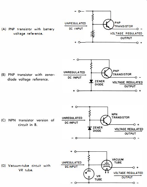
(A) PNP transistor with battery voltage reference, (B) Vacuum-tube circuit
with VR tube. Fig. 4-1 . Basic emitter- or cathode-follower voltage-regulator
circuits.
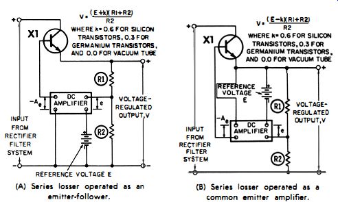
(A) Series loser operated as an emitter-follower. (B) Series loser operated
as a common emitter amplifier. Fig. 4-2. Two basic circuit arrangements for
series losser regulated power supplies.
The circuit in Fig. 4-2B makes use of X1 as a common-emitter amplifier. Here again, a second look may be necessary. X1 does not appear as a conventional common emitter amplifier inasmuch as the output circuit is associated with the emitter rather than the collector. Nonetheless, it can be readily seen that all criteria for common emitter operation are satisfied; the amplifier error signal is introduced at the base with respect to the emitter of X1. Moreover, from a dynamic standpoint, output variations actually occur in the collector circuit with respect to the emitter. The emitter is common element to one side of both input and output voltage variations.
It is interesting -to compare the two configurations. It might initially appear that the common emitter arrangement, by virtue of its inherent voltage amplification must make better use of a given number of power supply elements than the emitter follower which provides no voltage amplification. However, things do not actually work out this way.
The common-emitter stage exceeds the common-collector stage both in voltage gain and in output impedance by about the same factor. Voltage gain of the common emitter circuit is used up in reduction of its relatively high output impedance. Thus, dynamic output impedance of both circuits becomes about the same in the closed-loop regulator.
Often there are practical reasons which favor the use of one circuit over the other. For example, the comparator, DC amplifier stage (s), and particularly, the last DC amplifier stage (the DC stage which drives either the losser transistor or its associated Darlington stage) can be designed to handle voltages in the neighborhood of the emitter-base voltage of the common-emitter type losser. This is true even though the output terminal voltage of the regulator may be quite high. Conversely, with the common-collector (emitter follower) type of series losser, the DC amplifier stages must either be designed to withstand approximately output terminal voltage or must be protected from it. The latter-design technique can be accomplished for the last DC voltage amplifier stage by inserting a high-voltage zener diode in its collector lead. The zener diode "soaks up" most of the DC voltage without degrading amplification.
On the other hand, for low and medium output voltages, say under 30 or 40 volts, the common-collector series losser may lead to more economical design because the overall phase requirements of the regulator can be met with one less DC stage (in most designs) than required in the regulating circuit employing a common-emitter series losser.
In Fig. 4-2 k is the nominal forward-bias voltage required by the comparator transistor (or tube) associated with the divider network R1 and R2.
Often the nature of the series losser is obscured in the complexities of the regulator schematic diagram. When one terminal of the voltage reference element connects directly to the emitter of the series losser, the losser operates as a common-emitter type. When one terminal of the voltage reference element connects to the collector or to the supply lead not interrupted by the series losser, the losser operates as an emitter follower. Moreover, the common emitter series losser incorporates zero, or an even number of polarity-inverting DC amplifiers (excluding the losser itself) , whereas the emitter follower series losser achieves proper phase relationship with an odd number of such stages.
(However, when complementary symmetry is involved, the odd or even criteria loses its validity.) In most voltage regulators employing vacuum tubes as series lossers, the voltage requirements of all tubes are readily met with the "common collector" (cathode follower) configuration. For very high voltages, however, recourse is again made to common emitter mode of operation. With tube circuits the main precaution which ordinarily must be observed involves the insulation of the transformer filament windings. When the losser tube has a directly heated filament it is best to use a separate filament supply.
SHUNT VOLTAGE REGULATORS
Instead of being connected in series with one of the supply leads, the variable losser can be circuit-oriented to function as the shunt arm of a voltage divider. Two possible arrangements are depicted in ....

(A) Transistor circuit.
(B) Vacuum-tube circuit using VR tube. Fig. 4-3. Shunt voltage regulators.
... Fig. 4-3. In the transistor circuit (Fig. 4-3A) , any increase in output voltage will likewise increase the base-to-emitter bias in the negative direction. This increases the emitter-to-collector conduction of the transistor and thereby counteracts the increased output voltage. The tube circuit shown in Fig. 4-3B is not the exact counterpart of the transistor circuit, because here the VR tube is located in the cathode lead. Although the tube is not directly across the output terminals, the operation is essentially similar to that of the transistor circuit. An increase in output voltage increases the grid-to-cathode voltage in the positive direction, thereby causing heavier cathode-to-plate conduction.
In the transistor configuration (Fig. 4-3B) , such action increases the voltage drop across series resistance R, enabling the output voltage to remain almost constant. In these circuits, the variable losser functions as a cathode (or emitter) follower, the input being essentially the voltage drop across the reference element.
An important operating difference between series and shunt losser circuits is the no-load or light-load efficiency.
In the shunt type, the losser itself must assume the role of load in the absence of the external load. Thus, the efficiency of this type of regulator is very low when the current demand of the external load is not an appreciable fraction of the full-load current. Between half- and full-load, the efficiency is comparable to that obtainable from a similarly loaded series-type regulator. In transistor regulators, the shunt circuit has the advantage of being inherently short circuit-proof-a short across the output terminals merely removes the operating voltages. In contrast, a short circuit applied to a series regulator subjects the losser element to high voltage and high power dissipation. The voltage alone is often sufficient to destroy the series control transistor and, by a chain reaction, the smaller transistors if a DC amplifier is incorporated between the reference element and series control transistor.
CURRENT REGULATORS
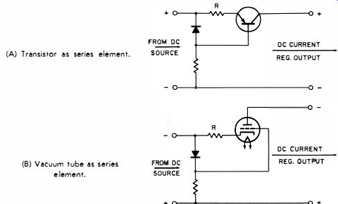
(A) Transistor as series element. (B) Vacuum tube as series element.
Fig. 4-4. Current regulators.
Configurations of some simple current regulators are shown in Fig. 4-4. Like the simple series and shunt voltage regulators described previously, these current regulators depend for their operation on a fixed reference voltage, feedback of an error signal, and power amplification in the losser element. Note that although current is the stabilized parameter, it is the voltage drop that is actually "sensed" and compared with the reference voltage. This voltage drop is developed across a small resistance, R. Being directly proportionate to the load current, this voltage drop can be said to faithfully represent the current flowing through the external load. Should the load current rise, the increased volt-age drop across R constitutes bias of the proper polarity to counteract the current increased. The converse sequence of events occurs if the load current decreases. The nominal value of stabilized load current can be varied by changing the value of R or inserting voltage reference sources with different fixed voltages.
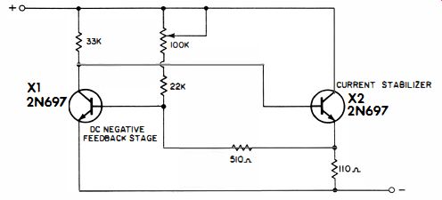
Fig. 4-5. Representative current regulator using DC negative feedback stage.
A somewhat different approach to current regulation is shown in the representative circuit of Fig. 4-5. Here the stabilizing action is not dependent upon a voltage reference element. The configuration comprises a two stage, direct-coupled amplifier with heavy negative feedback. The flow of current through current-stabilizer transistor X1 develops a voltage drop across the emitter resistance of that stage.
This voltage drop is amplified and inverted by the AC negative feedback stage X2 and then fed back to the base of X1.
The resulting closed loop action is control of X1 so as to oppose any change in its emitter-collector current. The result is that the applied voltage can vary over a considerable range with negligible change of current in the series connected load. The variable resistance is empirically adjusted to provide constant load current with respect to applied voltage. (By means of this adjustment it is possible to have the load current increase or decrease with respect to an increase in applied voltage.) As shown in Fig. 4-5, the circuit will maintain a load current of approximately 5 milliamperes for applied voltages in the 5- to 25-volt range. Higher currents can be regulated by decreasing either or both the 110 ohm emitter resistance of stage X2 or the 33K collector resistance of stage X1. The plus and minus polarity designations are relative. The current regulator, voltage source, and load comprise a series circuit ; their connection sequence is not important as long as the regulator "sees" the indicated relative polarity. A useful circuit feature of this type of current regulator is that it is effectively a two terminal circuit. Thus, it can be packaged and utilized as a constant current "diode" in an analogous manner to the constant voltage zener diode. PNP transistors can be substituted if the appropriate changes are made in terminal polarity.
With larger transistors, particularly for X2, the circuit can be designed to regulate much heavier currents much more closely.
A family of high current germanium power transistors (PNP) are depicted in Table A-2 in the Appendix. These Honeywell units maintain a minimum current gain of 15 up to collector currents of 65 amperes. This is a very worthwhile characteristic, for it is often found that a power transistor begins to suffer appreciable loss in current gain long before its power dissipation rating is exceeded. When this happens, the transistor becomes less responsive to the amplified error signal and the performance of the regulator is degraded.
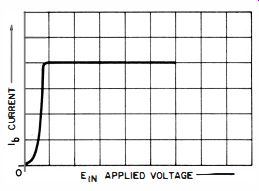
Fig. 4-6. The volt-ampere characteristic of the Currector.
Commercial two-terminal current regulators are available. These are manufactured both from discrete components and from monolithic semiconductor material. One such device, known as the Currector is made by the Circuit-dyne Corporation. A typical current-voltage relationship of a Currector is shown in Fig. 4-6. Such devices are very useful for providing constant current to differential amplifiers. When so used, the constant current device is connected in place of the mutual emitter resistance. A differential amplifier so connected will perform well from a relatively low-voltage supply. Superior common mode rejection and improved temperature stability are obtained compared to operation with the emitter resistance. The basic idea is depicted in the representative circuit of Fig. 4-7.

Fig. 4-7. Representative differential amplifier with constant current source
in place of resistance.
Two-terminal current regulating devices can be used to upgrade the performance of voltage-regulated power supplies. In the simplest of such applications, the current regulating device substitutes for the series dropping resistor in an open-loop zener diode supply. In Fig. 4-8 the voltage ...
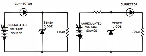
Fig. 4-8. Replacement of series loss resistance by Currector element in
zener regulated constant voltage supply. Fig. 4-9. Improvement of current
regulation by means of zener diode preceding the Currector element.
... regulation seen by the load is better than would be obtained with the conventional series dropping resistor. This is particularly true of load voltage with respect to variations in the unregulated supply.
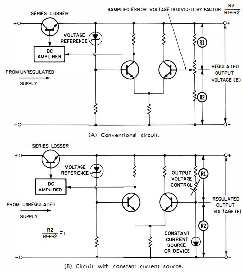
(A) Conventional circuit. (B) Circuit with constant current source. Fig. 4-10.
Simplified sampler/comparator circuits showing advantage of constant current
source in comparator section.
Probably the best use of this current regulator-zener diode combination is for achieving a more stable voltage reference in closed loop regulated supplies.
The converse situation is shown in Fig. 4-9. Here, enhanced current regulation ensues from the constant-voltage property of the preceding zener diode. Other useful combinations of constant-current "diodes" and constant-voltage diodes will, no doubt, suggest themselves to the imaginative experimenter.
In conventional closed-loop regulated supplies, the resistance voltage divider network provides a desired and an undesired effect. The potentiometer action of this divider permits an appropriate sample of the output voltage to be impressed at the comparator IDC amplifier for comparison with the stable reference voltage. However, this network also divides the available loop amplification. This situation can be circumvented by the arrangement shown in Fig. 4-10 where a two-terminal, constant-current source substitutes for the resistive arm of the sampling network which conventionally is connected to the un-sensed side of the supply.
Even though a resistance, R1 is used for control of output voltage, the sampled voltage is always substantially unattenuated. The constant current source is the equivalent of an extremely high resistance insofar as concerns potentiometer action of the sampling circuit. Nearly 100 percent negative feedback exists in the regulating circuit as a consequence of this. Another way of stating this is that virtually no amplification is wasted when such an arrangement is used. This is reflected as a lower, dynamic output impedance, generally the most important performance parameter of voltage-regulated power supplies. To derive optimum results with this technique, the emitter-base current of the sensing transistor should be a very small part of the stabilized current provided by the constant current source.
High performance voltage-regulated supplies usually have some provision for operating the collector of the last DC voltage amplifier from a constant-current source. This prevents injection of ripple into the base of the series losser or its Darlington connected driving stage. The most common constant-current circuit employs a "three" terminal transistor/zener-diode arrangement such as shown in Fig. 4-4A. In some cases, the pentode-like characteristic of a grounded-base transistor provides constant-current behavior for this purpose. (With a transistor so-used, no zener diode is needed ). It is probable that a two-terminal constant current source would serve this function equally well as the three terminal circuits.
ERROR-SIGNAL AMPLIFICATION
Up to now we have investigated several simple configurations for regulating the voltage or current of load powers beyond the practical or economical range of zener diodes or VR tubes. The power amplification contributed by the variable losser element improves the dynamic characteristics of the supply in all these circuits. Further improvement is readily attainable by increasing the power amplification in the feedback loop. This is done by inserting voltage amplifiers-and often in transistor regulators, current amplifiers--between the voltage reference and variable losser. With such a scheme, the ,control function becomes sensitive to very small changes in output voltage or current. Other advantages are also obtained-both design and operational flexibility prosper from such an arrangement. For example, the output voltage can readily be made controllable and independent of the fixed reference voltage. Thus, a 6-volt zener diode can stabilize output voltages from zero to several hundred volts, any voltage within such a range being selected by a potentiometer. Contrary to the situation which prevails in simple supplies (where a potentiometer is provided for output control ) , the dynamic output impedance and output resistance of the regulator-amplifier combination can remain extremely low over the entire range of adjustable voltages.
DC AMPLIFIER PROBLEMS
Although the insertion of amplification between the sampled portion of the output voltage (or current) and the variable losser enhances the performance of the power supply, this scheme is not without its problems. One of the undesirable characteristics of DC direct-coupled amplifiers is their tendency to drift. A slight shift in operating point in the input stage is indistinguishable from an error signal. Such a shift will therefore change the output of the power supply, this change being unrelated to the stabilization. Under certain conditions, drift can become cumulative and result in a runaway condition. In any event, the presence of appreciable drift causes erratic hunting of the output level. This problem generally does not impair the performance of capacitor--or transformer-coupled AC amplifiers. For this reason, when precise stabilization is required, the error signal sometimes is interrupted by an electronic or electromechanical chopper and the resultant AC signal amplified by an AC rather than DC amplifier. This type of regulated power supply will be dealt with in more detail later. Our present concern is with techniques for minimizing drift in a DC amplifier.
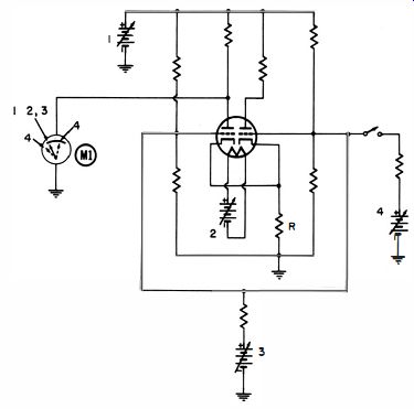
Fig. 4-11. Effect of operating voltage variations on output of differential
amplifier.
You will find that the inherent drift problems generally begin to assert themselves whenever two or more DC amplifier stages are cascaded. In such instances the drift in the input stage inflicts the most serious consequences, because it receives more amplification than the drift occurring in a second or third stage. For this reason, a great deal of attention has been given to the design and operation of the input stage. Transistors are particularly susceptible to drift from temperature changes. A very effective circuit for minimizing the input-stage drift of transistors and vacuum tubes is the differential amplifier in Fig. 4-11. Note that the two amplifying elements are physically close together-that is, in the same thermal environment. Thus, a change in the common filament temperature will not change the plate current and therefore the output-voltage level. Suppose the filament temperature is decreased, with the attendant tendency of the plate current in both tube sections to decrease. Because of the common cathode resistance, R, each tube will control the cathode-to-grid bias of the alternate tube. Any tendency of both tube sections to decrease their plate currents by the same amount will result in both cathodes being simultaneously driven less positive than their grids. In turn, conduction will increase in both tube sections. Because of the amplification in the tubes, the increased conduction (due to the cathode-to-grid bias ) very nearly offsets the decrease in conduction due to the lowered filament temperature. Therefore, the conduction of the tube sections remains fixed, and their output does not change. Here we see a regulatory action in which equal changes in the amplifying elements are canceled. Significantly, in a properly designed differential amplifier, most drift tends to take place within both amplifying elements.
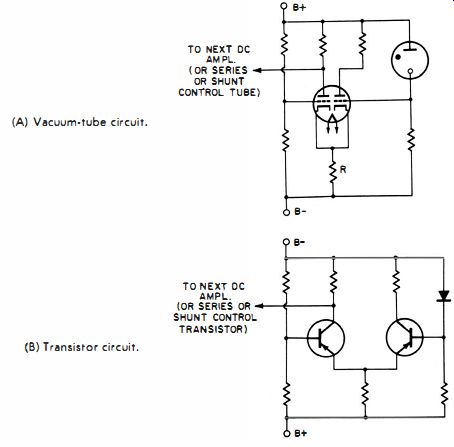
(A) Vacuum tube circuit. (B) Transistor circuit. Fig. 4-12. Typical examples
of differential amplifiers with input voltage reference connected to one
input.
Let's look at other "common mode" changes. The same signal, when applied simultaneously to both grids, is similarly prevented from changing the output-voltage level at the plates. The same is true for B+ variations. In summary, variations in voltages from sources 1, 2, and 3 in Fig. 4-11 produce no appreciable change in output voltage as seen on meter Ml. A change in output voltage does occur, however, if the bias on either one or the other (but not both) grids is changed. Now, in Fig. 4-12, B+ variations will change the output voltage because one of the control elements is connected to a voltage reference element. Such an arrangement does not result in both grids or both bases receiving a common-mode signal. An output signal then is developed which is the amplified difference between the voltage levels applied to the two grids or bases. Such operation is desired when the differential amplifier is used as an error-signal amplifier in the feedback loop of a regulated power supply. Fig. 4-12A illustrates the vacuum-tube circuit and Fig. 4-12B the equivalent transistor configuration.
Transistors present more of a problem in the differential amplifier than vacuum tubes. This is primarily due to the matching and tracking problems inherent in transistors.
In the first place, transistors bearing the same type designations often differ from one another more than two vacuum tubes of different type designations. Even if a pair of transistors are matched at room temperature, some of their characteristics can diverge considerably as the temperature rises.
This is particularly true of the collector saturation current ; it is generally far better to use transistors with very low collector saturation currents than to attempt to match two transistors having appreciable collector saturation currents at room temperature. For this reason, silicon transistors are preferable to germanium transistors for the differential amplifier. Additionally, the two transistors should have as nearly identical current gains and base-to-emitter voltage characteristics as possible. Both transistors should be mounted in a common heat sink-despite the fact that dissipation will normally be quite low-because the heat sink ensures an identical thermal environment for both transistors.
The Fairchild transistors shown in Table A-4 and A-5 in the Appendix may be considered as "work-horse" types for regulator circuits. These transistors are of silicon planar construction and possess excellent characteristics. Note that they are available in both NPN and PNP polarities. The author particularly recommends the 2N966 and 2N967 NPN transistors and the 2N1131 and 2N1132 PNP transistors.
These transistors can be directly substituted for a great number of germanium transistors specified for such circuit functions as comparator, differential amplifier, voltage amplifier, and Darlington driver.
Complete differential amplifiers within a single package are now available. These have the important feature that both elements are exposed to very nearly the same thermal environment. A list of such differential amplifiers made by Fairchild appears in Table A-6 in the Appendix. It will be observed that differential amplifiers corresponding to both NPN and PNP transistors are available.
Somewhat similarly, Darlington amplifiers are packaged within one container. This gives the effect of a single transistor with extremely high current gain. Three Fairchild units are shown in Table A-7 in the Appendix.
Epoxy encapsulated silicon planar transistors are available which, in many instances, provide all the attributes of silicon transistors but at considerably lower price than conventional TO-5 and TO-18 packaging. These transistors are' "passivated" by means of a silicon-oxide surface film, so that they are not primarily dependent upon the epoxy seal for protection from moisture and atmospheric gasses. Some of these types have exceedingly high current gain (beta) ratings. Epoxy has good thermal conductivity and for a few cents additional outlay, a simple clip-on heat sink will provide increased power dissipation capability. Table A-8 lists a series of General Electric NPN types. Fairchild makes both NPN and PNP types with epoxy encapsulation; these are shown in Tables A-9 and A-10 in the Appendix.
Table A-11 (in Appendix ) lists a series of Fairchild temperature compensated reference diodes. These have very low temperature coefficients. By their use, great stability of regulated output voltage or current is readily obtained with respect to temperature.
Although elaborate precautions are prescribed for balancing the two amplifiers in the differential circuit, the two plate-load resistors need not be equal in resistance, because the plate or collector current is determined primarily by the bias at the cathodes or emitters. Consequently, we often see unequal plate or collector resistances, and sometimes one of them is omitted.
OSCILLATION SUPPRESSION
The DC amplifier is an AC amplifier as well. This is desirable, for it enables the over-all regulator circuit to provide electronic filtering of residual ripple from the unregulated power supply. However, the effect of the amplification in lowering the dynamic output impedance cannot extend to higher frequencies than those to which the amplifier will provide appreciable gain. Inasmuch as high amplification in the error-signal feedback loop is a relatively cheap way to enhance the performance of a regulated supply, it is commonplace to provide fairly high gain in all but the most rudimentary regulators. This, however, introduces the possibility of oscillation. Although the feedback is negative at DC and low frequencies, cumulative phase shifts in the amplifying elements generally are such that the criterion of oscillation is met at some sufficiently high frequency. When such oscillation occurs, the AC generated can exceed the permissible voltage swing at the input of one or more amplifying elements. As a result, rectification takes place, with the attendant shift in operating point of the amplifier stages. This amounts to a condition of enforced drift that incapacitates the regulator. In transistor amplifiers, destruction of transistors is not an uncommon occurrence. Even if the oscillation is weak, it will still impair the regulator performance by appearing across the output terminals. In the interest of proper regulator operation, it is most important that any oscillation or tendency toward oscillation be suppressed.
Oscillation can be either caused or inhibited by actual, stray, or equivalent reactances in certain portions of the amplifier circuit. The most straightforward remedy is to connect capacitors at the appropriate junctions, to prevent phase-gain conditions for oscillation. Such capacitors will be observed in the ensuing circuits of regulated power supplies.
Where feasible, they are connected to high-impedance points; this permits the use of a comparatively small capacitor.
Sometimes it is necessary to connect a large electrolytic capacitor directly across the output terminals in order to discourage oscillation at all frequencies.
Oscillation problems are generally agitated in voltage regulated supplies designed to provide a considerable range of control over the output voltage. The reason is that zero output voltage is approached as the negative feedback is increased (by adjusting the potentiometer in the output voltage sampling network) . The potentiometer is adjusted in the direction which makes the sampled voltage a larger fraction of the output voltage than would be true for higher output voltages. It is well known, from audio-amplifier techniques, that a practical limit is reached in the amount of negative feedback which can be incorporated. This practical limit corresponds to the occurrence of oscillation at those frequencies where gain and phase conditions actually produce positive feedback, thus converting the amplifier to an oscillator. Other things being equal, such conditions tend to manifest themselves as the amplifier gain and feedback factor are increased. In the voltage-regulated supply, the feedback factor increases as the supply is adjusted toward a lower output voltage.