AMAZON multi-meters discounts / AMAZON oscilloscope discounts
The primary purpose of semiconductors, or solid-state devices as they are sometimes called, is to control the flow of electrons. They can be employed in almost any application that a tube can, and in some where a tube cannot.
WHAT IS A SEMICONDUCTOR?
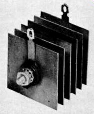
Fig. 1. A selenium rectifier.
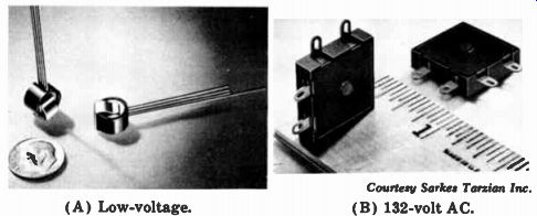
Fig. 2. Selenium bridge rectifiers. (A) Low-voltage. (B) 132-volt AC. Courtesy
Sarkes Tarzian Inc.
When properly treated, certain materials such as germanium, silicon, and selenium have the unique property of al lowing electrons to flow through them in one direction, but not in the other. They therefore act like a conductor in one direction, but like an insulator in the other. Hence the name, "semiconductor." Unlike vacuum tubes, the semiconductor material is solid-there is no need to separate the various parts by a vacuum or gas. In some, the entire unit is composed of the same type of material. In others, the materials are different but are still in physical contact with each other.
Connections are then made at the proper places, and a protective covering placed over the entire assembly.
RECTIFIERS
The power rectifier is the simplest and oldest of the semiconductor devices. It performs essentially the same function as a diode tube. In the power supplies of radio and television receivers, for example, it converts the AC line voltage into the DC needed to operate the various stages. The oldest type of metallic rectifier used in entertainment-type equipment is made of selenium, a typical unit of which is pictured in Fig. 1. The desired rating is determined by the number of plates. Two other types of selenium rectifiers are pictured in Fig. 2. Each of these units actually contains four separate power rectifiers connected together. Note their small size.
Silicon rectifiers (Fig. 3) are also very popular. A silicon unit is usually much smaller than a selenium unit. Connections are usually soldered directly to selenium rectifiers; however, silicon units may be plugged into a holder (Fig. 3A) or soldered in the circuit (Fig. 3B) . Others are en closed in containers (Fig. 4) which can be plugged into conventional tube sockets. Units of this type are designed to directly replace tubes.

Fig. 3. Silicon rectifiers. (A) Plug-in. (B) Solder-in. Courtesy Sarkes
Tarzian Inc.
The symbol adopted for power rectifiers is given at A in Fig. 5. In some instances, part of the symbol will not be shaded, as shown at B and C, or the entire symbol may be left unshaded, as shown at D. Symbols E and F are rarely used.
The bar portion in symbol A corresponds to the cathode of a vacuum tube. That is, electrons flow from it toward the arrowhead. This bar portion will sometimes be labeled with a "+" sign or the letters CATH. The same markings may be stamped on the unit itself.
Letter Codes
There is much disagreement among manufacturers about which letters to use in designating power rectifiers. Consequently, the letters M, CR, SE, X, Y, E, and REG, among others, may be encountered.
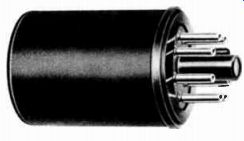
Fig. 4. A silicon rectifier designed to plug into a tube socket. Courtesy
Sarkes Torsion Inc.
SIGNAL DIODES
Like power rectifiers, signal or crystal diodes perform the same function as a diode tube. The difference between the power rectifier and the signal diode, however, is in the function each performs in a circuit. Power rectifiers are used in power-supply circuits to handle large amounts of current. Signal diodes are used in signal circuits and thus they pass only small values of current. Typical signal diodes are shown in Fig. 6. Some have leads that are soldered into the circuits; others are plugged into a holder.
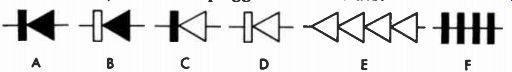
Fig. 5. Power-rectifier symbols.

Fig. 6. Crystal diodes.
The symbols for signal diodes are the same as those shown at A, B, C, and D in Fig. 5 for power rectifiers. Sometimes the symbol may be enclosed in a circle. Symbols E and F, however, are never used for crystal units. Like power rectifiers, a "+" sign or the letters CATH are often placed near the bar portion of the symbols. Either marking may also appear on the end of the unit itself, although a colored dot or ring or some other identification is often placed there instead.
Letter Codes
Like the power rectifier, many letters are used to designate signal diodes. Some of those used are D, E, SC, CR, XD, X, and Y.
TRANSISTORS
In 1948, Drs. William Shockley, John Bordeen, and Walter H. Brattain of Bell Telephone Laboratories announced their development of the first transistor. Since that time, the transistor has revolutionized the electronics industry. It can be used in practically every application that a tube can be --and in some it can't--but, as was once prophesied, has not replaced tubes. They are still better suited for certain applications.
Fig. 7. A composite group of transistors. Courtesy Philco Corp.
The principal advantages of the transistor over a tube are: (1) it is much smaller; hence, equipment can be made much more compact ; (2) its power requirements are much lower, so large power supplies are not needed; in fact, a small flashlight cell will operate a transistor for a long time; (3) it has no heater; this further simplifies the power supply and reduces ventilation problems; and (4) it has a longer life expectancy and is less fragile.
The word "transistor" is a broad term applied to the entire field of those semiconductor devices which have three or more terminals. Fig. 7 shows some of the many sizes and shapes available. Each has its own particular application where it performs the same function as a vacuum tube- amplifying, mixing, oscillating, and switching, to name a few.
Transistor Construction
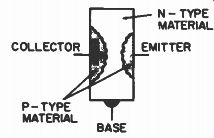
Fig. 8. Elementary construction of a transistor.
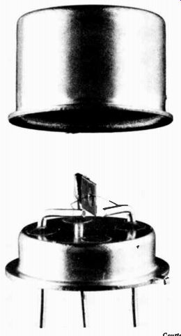
Fig. 9. An enlarged view of a transistor with cover removed. Courtesy Philco
Corp.
In function, the transistor corresponds roughly to the triode vacuum tube. Fig. 8 shows the construction of a typical transistor. It consists of a slab of semiconductor material to which connections are made at three points.
Notice that the material at the points where two of the connections are made is labeled P-type and the remainder of the slab is labeled N-type. The adding of certain impurities to the semiconductor will alter its electrical properties. If, as a result, the material contains an excess of electrons, it is called N-type ; if it has a deficiency, it is called P-type. Notice in Fig. 8 that the two areas of P-type material are separated by an area of N-type. A view of a typical transistor with the cover removed is given in Fig. 9. Connection to each of the different areas of the semiconductor slab is taken out to leads at the bottom. This shows a PNP-type silicon transistor, and to give you an idea of its size, the cap is approximately three-tenths of an inch in diameter-only slightly larger than the eraser on the end of a pencil! When the proper voltages are applied, electrons will flow through the unit, much as they do through a vacuum tube.
Since the unit in Fig. 8 consists of two areas of P-type material separated by an area of N-type material, it is called a PNP transistor. This order can be reversed during the manufacturing process, so that the two areas on the outside are N-type materials and the area in the middle is a P-type.
Now it is an NPN transistor.
The names of the three transistor elements are also given in Fig. 8. The emitter corresponds roughly to the cathode of a vacuum tube; the base, to the grid; and the collector, to the plate. However, electrons do not flow through the two types of transistors in the same direction. In the NPN type they flow from the emitter to the base and collector, whereas in the PNP type they flow from the collector and base to the emitter. Likewise, the voltages which must be applied to the collectors of the two types differ. The base of an NPN transistor must be more positive than the emitter, whereas for a PNP it must be more negative. In either instance, however, the difference between the voltages at the base and emitter will be only a few tenths of a volt.
Transistor Symbols
The symbols for an NPN transistor are given in Fig. 10.
Notice that the arrowhead may be located at the point where the diagonal intersects the circle, as in A, or placed along the line as in B. The element with the arrowhead denotes the emitter, and the bar portion of the symbol, the base. The remaining element is the collector. The letters E, B, and C identify the elements. The emitter is shown at the top of symbol C. Even when the different elements are repositioned, the emitter is always the element with the arrowhead. The symbols at D and E are seldom encountered.
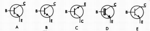
Fig. 10. NPN-transistor symbols.
Fig. 11 shows the symbols for a PNP transistor. The only difference is in the direction of the arrowhead. In the NPN transistor symbol it points away from the base, while for a PNP it points toward the base. In other words, it will always point in the direction opposite the flow of electrons.
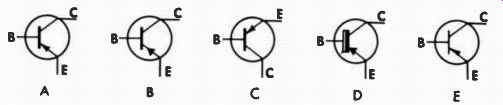
Fig. 11. PNP-transistor symbols.
(In transistor terminology this is called the direction of hole flow.) As with tube symbols, the circle denoting the protective covering is sometimes omitted, but this is not recommended.
Code Letters
Fewer letters are used to denote transistors of the various manufacturers than for other members of the semiconductor family. Nevertheless, the letters Q, X, V, T, and TR are presently employed.
OTHER SEMICONDUCTORS
There are many other types of semiconductors in use today. Some are not presently being used in consumer equipment, but no doubt you will encounter several of them as you examine various circuits. Only the more common will be discussed here.
Zener Diode
The zener diode is much like the power or signal diodes discussed previously. Its characteristics are very similar to those of power or signal diodes. Recall that a diode allows current to flow in only one direction. In the reverse direction, the diode has a high resistance. However, if a voltage higher than that at which the diode is designed to operate is applied in this direction, the diode will break down and current will flow. A normal diode may be damaged under these conditions; the zener diode is designed to operate in this manner.
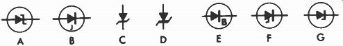
Fig. 12. Zener-diode symbols.
In operation, the zener diode serves as a voltage regulator; that is, when the voltage exceeds a given amount, the zener diode conducts, limiting the voltage to the desired value.
Fig. 12 shows the symbols used to denote a zener diode.
Those at A and C are probably the most popular. Any of the symbols can have the circle as at A, B, E, F, and G or with out as at C and D. The zener diode is also known as a back ward diode, breakdown diode, avalanche diode, and voltage regulator diode.
Silicon Controlled Rectifier
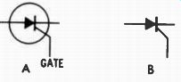
Fig. 13. Silicon controlled rectifier symbols.
The silicon controlled rectifier (SCR), also called a thyristor, is actually like two transistors in construction. In operation, it is similar to the thyraton discussed in Section 5. The symbols used to represent an SCR are very similar to those for the diode, as shown in Fig. 13. In operation, the diode will not conduct until a "trigger" current is applied to the added connection, called the gate. Silicon con trolled rectifiers are used mostly in AC control applications.
They are presently widely used in lighting control and power tools.
Tunnel Diode
In the normal semiconductor, it takes a certain amount of time for the current carriers to move through the unit.
Fig. 14. Tunnel-diode symbols.
In the tunnel diode, however, they appear to move at the speed of light-according to Einstein's theory, the ultimate speed in the universe. At the same time, a tunnel diode is capable of amplifying-a function not normally obtained in a two-element device. Explanation of the tunnel diode is beyond the scope of this guide. Tunnel diodes can be used in many types of circuits where usually only a transistor or tube can be used. Temperature extremes and nuclear radiation have little effect on them. Fig. 14 shows the most common symbols used to depict a tunnel diode on schematics.
As with other semiconductor symbols, the circle may or may not be used.
Capacitive Diode Also called a varactor, Varicap, reactance diode, or parametric diode, the capacitive diode actually functions as a capacitor in the circuit. The symbols for this device are given here instead of in Section 3 because most of the symbols used to depict it (Fig. 15) resemble those for the semi conductor diode. Recall that a semiconductor diode consists of a layer of P- and a layer of N-type material. When these two materials are joined, a layer forms at the junction which serves as an insulator. This condition is the same as for a capacitor-two conductors separated by an insulator. In the normal diode, steps are taken to minimize this capacitance.

Fig. 15. Capacitive-diode symbols.
In the capacitive diode the capacitance is emphasized. The capacitance of a capacitive diode will vary, depending on the voltage across the diode. Thus, by varying the voltage, the capacitance varies, and a circuit can be "tuned." The greatest use of varactors has been in high-frequency applications, but they can be used in any application where a variable capacitor is called for. The limiting factor is the small degree of change in the capacitance of a capacitive diode, but recent developments indicate that this range can be increased.
Photodiodes
The semiconductor diode is a very versatile device. There seems to be no end to the uses to which it can be put by simply varying the construction and composition. Silicon diodes are also sensitive to light. In some applications they function as a resistor whose value varies according to the amount of light striking it. In this use, they are usually called light-dependent resistors. Symbols for this use were given in Fig. 2-13.
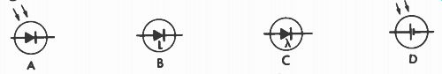
Fig. 16. Solar-cell symbols.
In addition, a voltage can be generated when light strikes the diode. In this application it is called a solar cell. Fig. 16 shows symbols used to depict the solar cell. The symbols at A, B, and C resemble the diode symbol with the arrows, letter L, or Greek lambda ( lambda) signifying that it is light sensitive. The symbol at D more nearly represents a battery (to be discussed in a later section). As with other diode symbols, the circle enclosing the symbol may or may not be employed, but it is recommended.
Other Transistors
Several other types of transistors have been developed to serve applications. In operation, these units serve many special purposes, some of which cannot be obtained with vacuum tubes. The operation of such units is beyond the scope of this guide, but Fig. 17 gives the symbols for several "special" transistors. The symbol at A is for an N-type unijunction transistor, which essentially has two bases and an emitter but no collector. The symbol at B is for a P-type unijunction transistor. Other names for this device are double-base diode and filamentary diode.
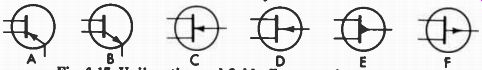
Fig. 17. Unijunction and field-effect transistor symbols.
The symbols at C and D in Fig. 17 are for an N-type- base field-effect transistor, while those at E and F are for P-type units. The field-effect transistor resembles a vacuum tube in its operation. Other semiconductors are essentially "current-operated" devices. That is, the electron (or hole) flow is the controlling factor. In vacuum tubes and field effect transistors, the controlling factor is the voltage.
QUESTIONS
1. Name two semiconductor materials.
2. Why must a semiconductor be enclosed in a vacuum?
3. What are the two principal types of transistors?
4. What are the three elements of a transistor?
5. What code letters are used to identify transistors?
6. Draw the symbol for a power rectifier.
7. Draw the symbol for a crystal diode.
8. Draw the symbol for an NPN transistor and label the various elements.
9. Draw the symbol for a PNP transistor and label the various elements.
10. Name an important application of zener diodes.