The microprocessor is a large, complex integrated circuit (IC) containing all of the computation and control circuitry for a small computer. It provides economical computing power for many devices including home computers, TV remote control units, electronic tuners, cash registers and video games. Let's now look at the general operation of the microprocessor systems and associated building blocks.
DEVELOPMENT OF THE MICROPROCESSOR
The earliest electronic computers were built using thousands of vacuum tubes. These devices were very large and unreliable, and were mostly a laboratory curiosity. The next generation was built with transistors, which made computers much more reliable and reduced their size and cost. These "solid-state" machines marked the beginning of the computer as a practical device.
In the 1960s smaller, more powerful computers were built using hundreds of gates, flip-flops, and other similar integrated circuits. These ICs are called small scale integration (SSI) devices. As semiconductor technology developed, it became possible to put dozens of gates on a single IC. Examples of these medium scale integration (MSI) ICs are counters, decoders, registers, and adders.
This down sizing continues, and in 1971 the first microprocessor (the 4004) was introduced. Microprocessors contain the major computation and control sections of a computer, called the-Central Processing Unit (CPU), on a single integrated "chip." Microprocessors are often called microprocessing units (MPUs). A microprocessor chip contains thousands of gates and is called a large scale integration (LSI) device. LSI memory devices were also developed that store thousands of bits of digital information on a single IC. These two LSI devices made it possible to drastically reduce the total size and cost of small computers. Microprocessors have made it practical to build dedicated computers into many small, inexpensive products.
MICROPROCESSOR USE
Microprocessors are now being used in many products which were previously built with random logic devices. Microprocessor-based de signs are usually less expensive and contain fewer components than the designs that they replace. Small microprocessor systems may be built with one or two ICs, at a cost of under ten dollars. These can often replace boards with dozens of simpler ICs. Because the number of discrete components and interconnections is greatly reduced, reliability is also improved.
This reduction in size is also possible using custom integrated circuits instead of microprocessors. However, the design of a custom IC can be an extremely complex and expensive process, often costing well over $100,000. This expense can be justified only for high volume products where the development costs can be spread over many thousands of units.
The microprocessor allows standard ICs to be used to achieve the same miniaturization. The customizing takes the form of the program stored in the memory. Producing a standard memory with a custom program stored in it is a relatively inexpensive process.
The flexibility and power of microprocessor based systems makes many sophisticated features possible, which in the past were impractical.
For example, microprocessor based systems can often test themselves to a considerable degree and give out error warnings. The microprocessor also makes practical the use of a keyboard instead of front panel switches.
Another feature is the capability for complete remote control.
A BASIC MICROPROCESSOR SYSTEM
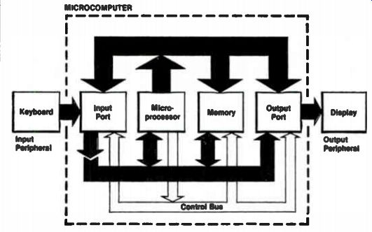
Fig. 1. Block diagram of microprocessor system.
Think of a system with a keyboard and a numeric display, as in a pocket calculator. When a key is pressed, the corresponding number should appear on the display. This system is a natural application for a microprocessor, and in many ways similar to a mini-computer.
You will note in Fig. 1 a block diagram of a system for doing this.
The microprocessor (also called the processor) is the "brains" of the system. It contains all of the logic to recognize and execute the list of instructions (program). The memory stores the program, and may also store data.
The microprocessor needs to exchange information with the keyboard and display. The input port, from which the processor can read data, connects the processor to the keyboard. The output port, to which the processor can send data, connects the processor to the display.
The blocks within the microcomputer are interconnected by three buses. A bus is a group of wires which connect the devices in the system in parallel. The microprocessor uses the address bus to select memory locations or input and output ports. You can think of the addresses as post office box numbers; they identify which locations to put information into or take information from.
Once the microprocessor selects a particular location via the address bus, it transfers the data via the data bus. Information can travel from the processor to the memory or an output port, or from an input port or memory to the processor. Note that the microprocessor is involved in all data transfers. Data usually does not go directly from one port to another, or from the memory to a port.
The third bus is called the control bus. It is a group of signals which are used by the microprocessor to notify memory and I/O devices that it is ready to perform a data transfer. Some signals in the control bus allow I/O or memory devices to make special requests from the processor.
A single digit or binary information (1 or 0) is called a bit (a contraction of binary digit). One digital signal (high or low) carries one bit of information. Microprocessors handle data not as individual bits, but as groups of bits called words. The most common microprocessors today use eight-bit words, which are called bytes. These microprocessors are called eight-bit processors. For an eight-bit processor, byte and word are often used interchangeably. Be aware, however, that word is also used to mean a group of sixteen or more bits.
Programs A program is required by the system to perform the desired task. In the following example are some of the instructions required:
• Read data from the keyboard.
• Write data to the display.
• Repeat (go to step 1).
For the microprocessor to perform a task from a list of instructions, the instructions must be translated into a code that the microprocessor can understand. These codes are then stored in the systems memory. The microprocessor begins by reading the first coded instructions from the memory. The microprocessor decodes the meaning of the instructions and performs the indicated operation. The processor then reads the instruction from the next location in memory and performs the corresponding operation. This process is repeated, one memory location after another.
Certain instructions cause the microprocessor to jump out of sequence to another memory location for the next instruction. The program can therefore direct the microprocessor to return to a previous instruction in the program, creating a loop which is repeatedly executed.
This enables operations which must be repeated many times to be performed by a relatively short program.
Peripherals
A complete microprocessor system, including the micro processor, memory, and input and output ports is called a microcomputer.
The devices connected to the input and output ports (the keyboard and display for example) are called peripherals, or input/output (I/O) devices.
The peripherals are the systems interface with the user. They may also connect the microcomputer to other equipment. Storage devices such as tape or disc drives are also referred to as peripherals.

Fig. 2. Three-State Driver and Truth Table.

Fig. 3. Equivalent Three-State Driver.
THREE-STATE DRIVERS
All devices in the microprocessor system exchange information with the microprocessor over the same set of wires (the data bus). The microprocessor selects one device to place data on the data bus and disconnect the others. It is the three-state output capability of the devices on the bus that enables the processor to selectively turn devices on and off.
In Fig. 2 you will see the symbol and truth table for a three-state buffer (often called a three-state driver). The buffer has an output enable in addition to the usual input and output. When the enable is low the buffer acts just as an ordinary buffer. The signal at the input is transferred to the output. When the enable is high, on the other hand, the output of the device is essentially disconnected.
Looking at Fig. 3, you will see a conceptual equivalent circuit which generates the open state using a relay. The disabled (open) output state is often called the high impedance state. Refer to Fig. 4 for the schematic of a typical three-state output.
Three-state drivers are important because they allow many devices to share a single data line. This circuit allows any one of three different signals to drive one output. Only one driver's enable line may be low, and that device drives the output. If more than one driver were enabled, they would both try to drive the output. This condition is not allowed because the logic state of the output would be unpredictable.
Many devices, including microprocessors and memories, contain internal three-state drivers. These ICs have an output enable, often called chip select (CS) or chip enable (CE), which controls their output drivers.
All devices which put data on the data bus have three-state drivers on their outputs. The microprocessor generates control signals (part of the control bus) to enable the three-state drivers of the device from which it wants to read data. The three-state drivers of the other devices are disabled.
THE MICROPROCESSOR
Illustrated in Fig. 5 are the basic signals that connect to a typical microprocessor. There are sixteen address outputs which drive the output bus, and eight data pins which connect to the data bus. The data pins are bidirectional, which means that data may go into or out of them. Read and write are the control signals that coordinate the movement of data on the data bus.
The two signals shown on the left of Fig. 5 provide additional control functions. The reset input is used to initialize the microprocessor's internal circuitry. The interrupt input allows the microprocessor to be diverted from its current task to another task which must be performed immediately. The use of these signals, plus several others are also used.
The two connections at the top are for an external crystal, which is used to set the frequency of the oscillator in the microprocessor. The output of the oscillator is called the system clock. The clock synchronizes all devices in the system and sets the rate at which instructions are executed.
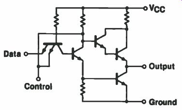
Fig. 4. Diagram of three-state driver.
MEMORIES ARE MADE LIKE THIS
Microprocessor systems usually use integrated circuit memories to store programs and data. They can store many bits of data in a single IC. Currently, devices are available with capacities well over 65,000 bits on one chip. A 65 K bit memory can store over eight thousand alphanumeric characters, or about three test pages on a piece of silicon about a third of an inch square.
The simplest memory device is the flip-flop, which stores one bit of information. Registers contain up to eight flip-flops on a single IC, each with its own data in and data out pins but with a common clock line.
LSI technology made it possible to put thousands of flip-flops on an IC, but a new problem was created. With thousands of flip-flops on an IC, there cannot be a separate data pin for each. The solution to this problem is to use address inputs to select the particular memory location (flip-flop) of interest. A decoder on the memory chip decodes the address and connects the selected memory location to the data pins.
Figure 6 shows a conceptual diagram of an eight-bit memory (most memories are much larger). Only the data output circuits are shown for simplicity. The decoder converts the binary address inputs to eight separate outputs, one for each possible combination of the three address lines. These signals control the three-state drivers at the output of each memory cell (flip-flop). The data from the addressed cell is placed on the data output line. This technique allows a single data pin to be used for all locations on the memory chip.
Each memory location can contain a group of bits rather than just one bit as in the example above. Each can hold one, or eight bits, depending upon the particular IC. If the IC has eight data pins, then each memory location stores eight bits of data. Note that while the memory may contain thousands of locations, only one may be accessed at a time.
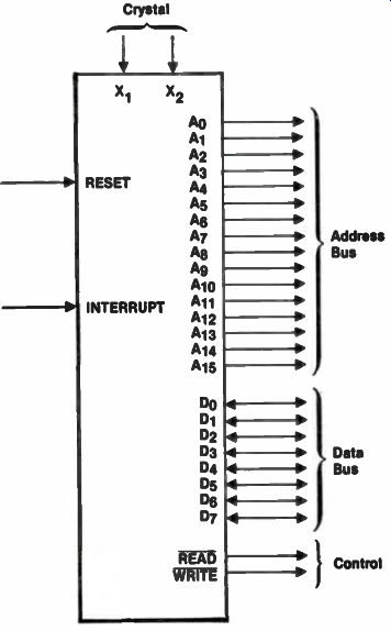
Fig. 5. Basic microprocessor signals.
The number of addressable locations depends upon the number of address lines. With one address line, two locations can be selected: address 0 and address 1. With two address lines, one of four locations can be selected: 00, 01, 10 and 11.
The memory ICs used with microprocessors fall into two broad categories: ROMs and RAMs. A ROM (read only memory) is a memory which can only be read. The data is programmed into it at the time of manufacture, or by a special programming procedure prior to installation in the circuit. A program recorded into a ROM is often referred to as firmware.
A RAM (random access memory) is a memory into which data can be stored and then retrieved. RAM is actually a misnomer; random access means that the time to access any memory location is the same, a characteristic also present in ROMS. Read/write (R/W) memory is a more accurate term for what are usually called RAMs, but RAM is widely used to mean integrated circuit read/write memory. A digital tape recorder is an example of a memory which is not random access, since the time to access a particular location depends upon the position of the tape.
An important characteristic of semiconductor RAMs is that they are volatile: they lose their data when power is turned off, and when turned back on, they contain unknown data. ROMs do not have this problem, so they are used for permanent program data storage. Since the contents of a ROM cannot be modified, RAMs must be used for temporary program and data storage.
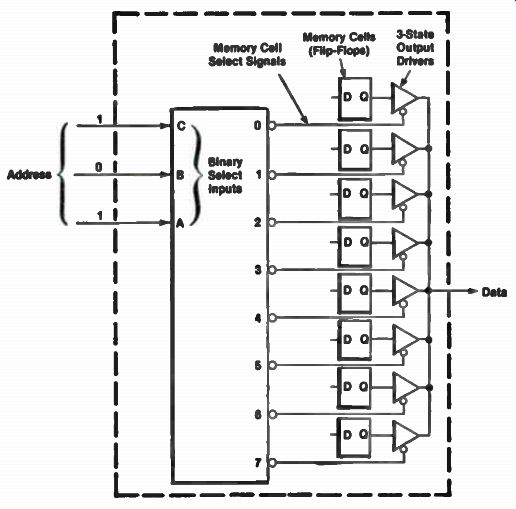
Fig. 6. Drawing of eight-bit memory.
Figure 7 shows a ROM containing 2,048 words of eight bits each, or 16, 384 bits. When using large numbers that are powers of two, "K" is often used to mean 1,024. Thus, this memory has 2K bytes of 16K bits.
Since each location contains eight bits, it is called a 2K x 8 ROM.
When the chip select input is low, the ROMs output drivers are enabled. When chip select is high, the data outputs are in the high impedance state. The three-state outputs allow the data lines of many memory devices to be connected together, with one device selected by bringing its chip select input low.
Illustrated in Fig. 8 is a 1K x 8 RAM. This RAM contains 1,024 locations of eight bits each. The data lines are bidirectional, since data can go into or out of the memory. RAMs have an additional control line called write. To store data in the RAM, an address is selected, the data is placed on the data lines, and the write line is brought low. When the data and address are all set, the chip select is pulsed, and the data is stored in the memory.
ROMs and RAMs come in many different sizes (with different numbers of words and different numbers of bits per word) and many types.
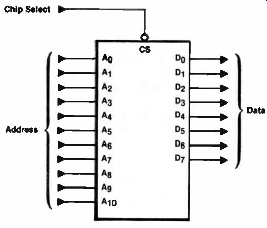
Fig. 7. A 2K x 8 ROM chip.
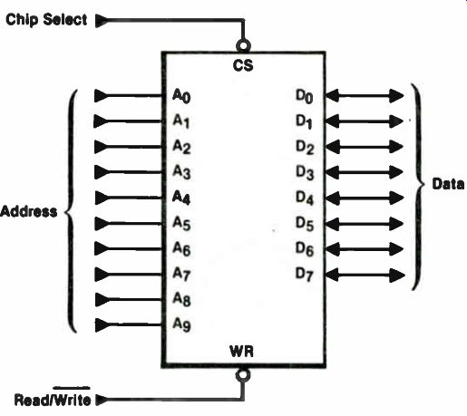
Fig. 8. Drawing of a 1k x8 RAM chip.
MICROCOMPUTERS AND MINICOMPUTERS
A microcomputer is functionally similar to a minicomputer, and, in fact, the distinction between the two is becoming less clear each day. A microcomputer's CPU (central processing unit) is the microprocessor. A minicomputer's CPU is usually a PC board with dozens of less complex, but faster, integrated circuits on it. The main functional difference is that minicomputers are usually faster. They also are larger and more expensive. As microprocessors have increased in speed and power to compete with the older minicomputers, new minicomputers have been developed which are even faster and more powerful. These new minicomputers often use microprocessors internally. Thus, while the basic distinctions of speed, power, and size remain, the exact boundary is becoming vague. Microcomputers are now finding applications in systems where a minicomputer would be too bulky and expensive.
RADIO SHACKS TRS-80 MICROCOMPUTER SYSTEM
In this section we will take a look at Radio Shack's very popular TRS-80 microcomputer system. Some brief system operation information will be given to help familiarize you with the system.
Troubleshooting information and tips will be given for the RAM, ROM, CPU, video divider chain, system clock, power supply, address decoder, address lines, keyboard and video processing system.
Also included in this Section are the complete diagrams for the TRS-80 and some section isolation troubleshooting flowcharts.
Let's now take a brief look at the basic operation of Radio Shack's model TRS-80 microcomputer. Some basic theory of operation along with block diagrams will be covered. Some troubleshooting tips and system flowcharts will also be investigated, and some power supply chart information. Plus hints, ideas, suggestions and other tips. A photo of the Radio Shack TRS-80 microcomputer system in operation is shown in Fig. 9.
IRS-SO System Block Diagram
You will find the integrated circuits contained in the TRS-80 can be broken down into ten major sections. The system block diagram in Fig. 10 shows these units as they are related to the other sections. The heart of the system is the CPU (central processing unit). Most of the leads on the CPU are data lines and address lines. The CPU tells the address bus where the data it wants is located, and the data bus is a good place for the information to come back to the CPU. The address lines are outputs from the CPU. They never receive data or addresses from other sections. The data lines on the other hand can give or receive data.
ROM Operation
If the CPU has to be the heart of the system, the ROM (read only memory) could very well be considered the brains. The ROM tells the CPU what to do, how to do it and where to put the data after each operation. Without the ROM, the CPU would just function or run as a pulse generator. When power is first applied to the system, the CPU outputs an address to the ROM that locates the CPU's first instruction. The ROM fires back the first instruction and then the two start communicating. In less than a second, the CPU, under ROM control, performs all the house-keeping required to start up the system and then flashes a "ready" on the screen.
li the CPU misses that first piece of ROM data, then it may become all fouled up. It may tell the ROM that it is ready to load a tape so that the ROM tells it how to do that. The tape recorder turns on. But since the CPU is now playing games in the video memory, the tape is not needed.
Because the CPU operates at about 2 MHz these digital foul-ups seem to occur instantaneously.
You can just think of the CPU as the work horse and the ROM as the boss. The ROM tells the CPU how to do it, when to do it, and where it was placed.
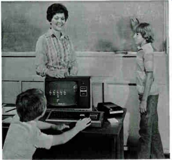
Fig. 9. The TRS-80 Radio Shack Microcomputer.
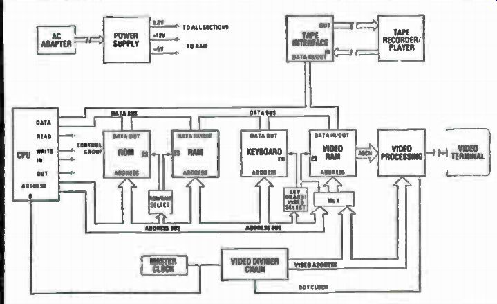
Fig. 10. System block diagram of TAS-80.
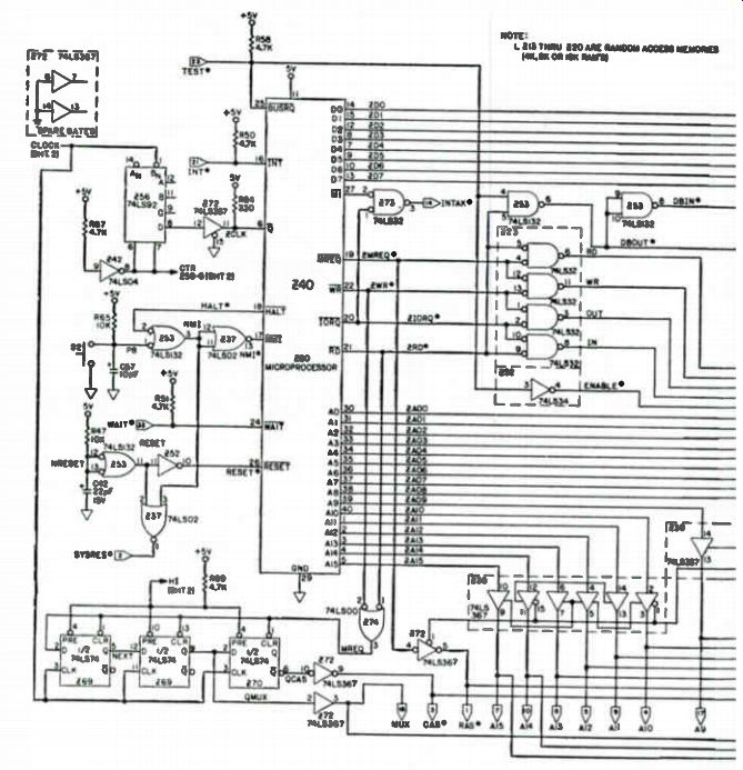
Fig. 11. Schematic of TRS-80 (section 1).
RAM Operation
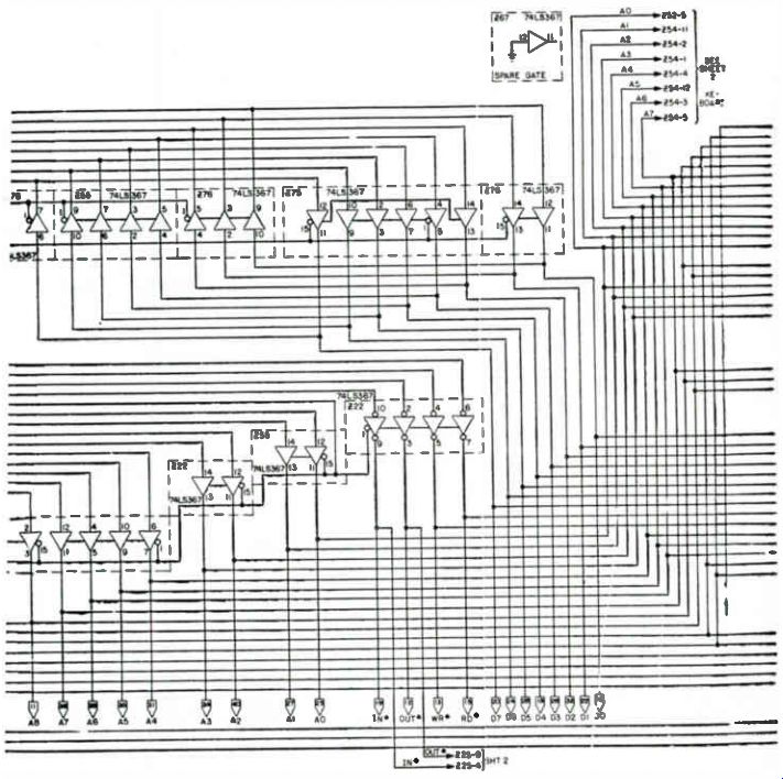
Fig. 11. Schematic of TRS-80 (section 1) (continued).
The next major section, see Fig. 11, is the RAM (random access memory). This memory is where the CPU can file data it may not need until later. The RAM is also the place where the programs are kept. If you tell the computer to count to 7,500, then the CPU stores your instructions in the RAM. The following occurs if you want the computer to act now.
The CPU tells the ROM someone wants in. The ROM tells the CPU to go to the keyboard and find out who. The CPU finds out, tells the ROM it's the number one chief. The ROM tells the CPU to find out what the chief wants. The CPU tells the ROM that the chief wants us to run. The ROM tells the CPU to go to the RAM and find out what the chief wants done. The CPU says the chief wants to count to 7,500. The ROM tells the CPU how to do it. After it's done, the ROM tells the CPU to find out what to do with it. The CPU informs the ROM that the 7,500 count must go on the video display screen and be saved. The ROM tells the CPU how to put it on the display and then tells it to store the 7,500 somewhere in RAM, then remember where it is. The CPU tells the ROM that the job is completed.
The ROM tells the CPU to monitor the keyboard in case the chief wants another program run.
The CPU looks to the ROM for instructions. The CPU then follows the ROM's instructions and looks to the keyboard, then the RAM. In all cases, the CPU applies address locations to the ROM, RAM and keyboard.
The data lines are then checked for input data that corresponds to these address locations. In case of an output from the CPU to RAM, the CPU selects the address, puts data on the data lines, and then instructs the RAM to store the data that is on the data lines.
Make a note, that only the CPU communicates with all other sections of the computer. If the CPU is told by ROM to store an item from ROM into RAM, the CPU can't make the RAM receive ROM data directly. Instead, the CPU takes the data from ROM and then sends it to the RAM. The CPU must act as intermediary between the two. The reason for this is that the CPU is the only section that can address locations and pass data to all other section.
Keyboard and Video Processing
The keyboard section is not necessary as far as the CPU is concerned, but it is very necessary for data to be fed in by the operator. The keyboard is used for making known your instructions to the CPU. The opposite is true for the video RAM. In this case, the CPU wants to tell us it needs data or it may want to show us the result of a complex calculation. So, the request for more information or the result is stuffed into the video RAM. Anything in video RAM is automatically displayed on the terminal screen.
The video processing section takes care of this. Data in the video RAM is in ASCII. Converting ASCII into the alphanumeric symbols we recognize is the task of the video processor. A ROM contains all of the dot patterns.
The ASCII locates the character pattern, and the video processor sends it out to the terminal screen.
Video Divider Chain
Composite video going to a video terminal is extremely complex.
Aside from the video signal, there is the horizontal and vertical sync.
These signals must be very stable and be outputted in the correct sequence. The CPU is very busy, so the video divider chain handles the TV signal to the monitor. It generates the sync signals and addresses the video RAM in a logical order so that the video processor can handle video data efficiently. Note the block under the video RAM labeled MUX. This is short for multiplexer. It acts somewhat like a multipole, multiposition switch. When the video divider chain is in control, the MUX is switched so that only addresses from the divider chain are directed to the video RAM. The CPU may need to read or write data into the video RAM. If so, the MUX is switched so that the CPU has control over the video RAM's address. After the CPU is finished, the addressing task is reassigned to the divider chain.
System Clock
The system clock circuit will be found in Fig. 12. Y1 is a fundamental-cut 10.6445 MHz crystal. It is in a series resonant circuit consisting of two inverters. Z42, pins 1 and 2, and 3 and 4, form two inverting amplifiers. Feedback between the inverters is supplied by C43, a 47 pf capacitor. R46 and R52 force the inverters used in the oscillator to operate in their linear region.
The waveform at pin 5 of Z42 will resemble a sine wave at 10.6445 MHz. The oscillator should not be measured at this point, however, due to the loading effects test equipment would have at this node. Z42, pin 6, is the output of the oscillator buffer. Clock measurements may be made at this point. The output of the buffer is applied to three main sections: The CPU timing circuit, the video chain, and the video processing circuit.
Address Decoder
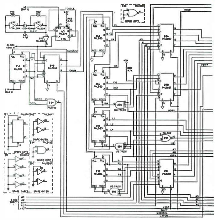
Fig. 12. Diagram of TAS-80 (section 2).
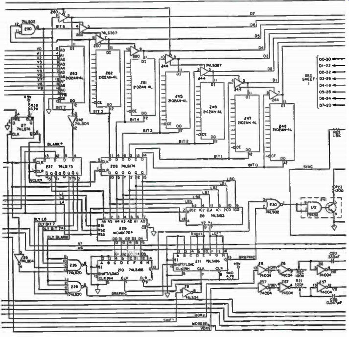
Fig. 12. Diagram of TRS-80 (section 2) (continued ).
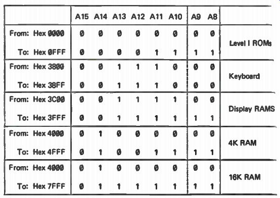
Fig. 13. Mapped memory for TRS-80.
The memory mapped chart for the TRS-80 is shown in Fig. 13.
Note that the address 01AC (in HEX) is in the ROM part of the map.
Address 380A is in the keyboard area and 3CAA accesses the video display RAMs. Since the data and address buses are connected in parallel to all the sections, there must be some method to determine which section is being accessed. A decoding network monitors the higher order address bits and selects which "memory" the CPU wants to use.
The address decoder (Fig. 14) is very important to the operation of the system. Refer to this schematic since there are signals that need to be sourced or traced.
The address decoder uses six bits, A10 through A15 are needed, plus RD and RAS (row address select). A15 is the most significant bit of the address bus. Let's combine the six high order bits and add a couple more, so that we have two hex digits: A15, A14, A13, A12, A11, A10, A9 and A8.
Al2 through Al5 form the most significant hex character. A8 through A9 are the two bits we had to add to complete that last hex character. Now let's break down part of the memory map into hex and binary. See Fig. 13.
Notice in the break down that we could use the two most significant digits of the hex code in the decoding scheme and handle the selection of all the memories. In the binary columns, you can see that instead of using two hex digits, which is eight binary lines, we can ignore two bits and use only six binary lines. A dotted line separates the two unused bits from the six that will be used.
Now look at Fig. 14 and you will see that bits Al2, Al3 and Al4 are connected to Z21, a dual, 2-input to 4-line decoder/demultiplexer. The C1 and C2 inputs are connected in such a way as to make Z21 into a 3-input to 8-line decoder. The G1 and G2 inputs connected to Z21 are chip enables.
As shown, when these inputs are at logical 0, Z21 is active. When high, Z21 is disabled and none of its eight outputs are low. The G-enables an controlled by OR gate Z73, pins 4, 5, and 6. Pin 4 is tied to A15, the mos significant bit of the address bus.
Referring back to Fig. 14, then A15 and RAS are low at the same time, a low will be outputted by Z73, pin 6. This low will enable Z21. When Z21 turns on, one of its outputs will go low, depending on the status of Al2 A13, and A14. For example, if these three inputs are high, pin 4 will e low. If all three inputs are high, pin 4 will go low. You might consider AL through A14 as supplying an octal address to Z21. Since there are eight states in an octal code, then there could be one of eight lines selected (output 0 through output 7). We can sum up Z21's function quite simply. It decodes the most significant digit of the hex address. Using Z21 and the last two bits, All and A10, we can define any one of the four "memories" available to the CPU in level 1. Address Decoder Programming Attached to the outputs of Z21 is X3. X3 is called a "dip shunt" and it is installed in the PCB position Z3. A dip shunt is like a shorting bar array, except the bars may be broken. By breaking some bars and leaving others intact, the address decoder is programmed to reflect the amount of RAM and ROM the CPU has available for use. You will note in Fig. 14, X3 is shown with six broken shorting bars.
Power Supply System
The TRS-80 requires three voltage supply levels as follows.
A +12 volts at 350 milliamps.
Fig. 14. Drawing of address de coder.
Also, +5 volts at about 1.2 amps.
And a - 5 volts at 1 milliamps.
The +12 and - 5 volts are needed by the system's RAM and all other devices that require +5 volts. The +12 volt and +5 volt supplies are regulated and current-protected against shorts. The - 5 volts supply is not as critical as the other two supplies, and it uses a single Zener diode for regulation. The stepped-down AC voltage is supplied by an "AC adaptor." The adaptor has a transformer with one primary and two secondary windings.
The secondary windings are both center-tapped. One is rated at 14 volts AC at one amp. This winding is used for the +5 and - 5 volt supplies.
The other winding had diodes connected and it outputs 19.8 VDC at about 350 milliamps. This circuit is used for the 12 volt supply. All voltage outputs and center taps are brought into the power input jack.
Unregulated DC voltage for the +12 volt supply is inputted at pin 2 of the power jack. When the power switch is closed the output voltage is about 20 volts due to action of the filter capacitor. This voltage is then fed to a transistor and regulator, Z2. Figure 12-15 shows a simplified diagram of the internal circuitry for the 723 regulator chip.
Referring to the circuit in Fig. 16, we see the filtered DC voltage from the adaptor and C8 is applied to pin 12 of Z2 and the emitter of series pass transistor, Q6. The voltage applied to pin 12 allows a constant current source to supply Zener current for Za. Pin 6 of Z2 will output a Zener voltage of about 7.15 volts. Pin 6 is tied to pin 5, the positive input to operate amplifier Zb. The negative input to the op-amp is tied to the wiper of R10. Initially, pin 4 of Z2 is at ground, forcing the output of op-amp Zb to output about 7.15 volts. Transistor Qa turns on, which turns on pass transistor Q6. The pass transistor supplies voltage for current monitoring resistor R18 and to the resistor network R13, R10 and R12. If R10 is adjusted for 7.15 volts at its wiper, the op-amp will be balanced and Q6 will output only enough voltage to keep the loop stable. If the output voltage dropped below 12 volts, Zb's output would decrease which would force the current through Qa to decrease. Qa would cause Q6 to increase the current through it, and the output would rise back up to the 12 volt level, ff the 12 volt line increased in voltage, the op-amp would cause Qa's current to increase, forcing Q6 to drop down.
Power Supply
Checks for the TRS-80 Most problems that result in loss of power supply voltage will be associated with solder shorts, component shorts or defective power supply adaptors. Usually, the power supply will not be damaged due to a short because the regulators use current-limiting with fold-back. A solder short or shorted component does not have to be in the power section to cause a supply problem. The short may be anywhere.
Should you be missing +12 volts and +5 volts, measure the voltage across R18. This resistor monitors the current flow from the +12 volt supply. If the voltage reads about 0.6 volts, the +12 volt bus is in fold-back and has shut itself off. Since the +12 volt bus is shut-off, you will not have +5 volts because the +5 volt regulator is referenced to the +12 volt output. You must now locate and remove the short on the +12 volt bus before anything will operate.
If the - 5 volt supply is not present, first confirm that there is ample negative voltage on the adaptor side of R19. See if R19 is dropping all of the voltage. If so, you have a - 5 volt bus short.
The +12 volt and the - 5 volt supplies are used by the RAM system. If you have problems with either of these two, suspect a RAM short. See if you can find a RAM that generates more heat than the others. Use a temperature probe for this check.
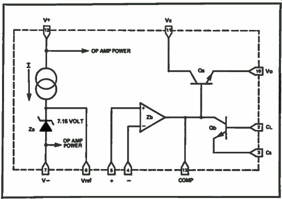
Fig. 15. Block diagram of 723 regulatorZ2.
Pull all RAM's and retest. If all of the power supplies are now good, turn off the power and re-install one RAM. Turn on the power and retest.
Install each RAM until you find one that loads down the power supply.
Remove the faulty RAM and continue to check out the other IC's. There may be more than one shorted device.
A short on the +5 volt bus can be a real tough one to find. Unless you can see the short, you will have to cut PC runs to isolate a section. Once a section is isolated you will probably have to make other cuts to find the short. And, remember to bridge the cuts when repairs are completed.
These runs carry considerable current, so use solid 22 gauge wire to bridge the cuts.
If you find a dead +12 volt bus, check transistor Ors heat sink. The hardware holding the transistors heat sink may have become loose and shorted Ors leads.
Figure 17 lists the voltages found around Z1 and Z2 for a normal operating unit. These measurements were taken when the +12 volt supply was adjusted for 12 volts and the - 5 volt supply was adjusted to 5 volts.
Isolation of a Defective Computer Section
One of the toughest problems to section-isolate is a screen full of junk at power on. This is a display with all character positions filled with either alphanumeric or graphics. Also, a garbage condition does not always indicate that the power-up logic is defective. A problem could exist in RAM, ROM, the video divider chain and of course the CPU itself. Thus, a fault could exist in 75% of the computer system.
You could start by replacing all of the RAM's, ROM's and the CPU but, this would be a waste of time. If the problem was a cold solder joint or a short, replacing all plug-in devices would not solve the problem. The section isolation technique will probably yield much more positive results.
This is based on a removal technique that eliminates sections from the suspect list.
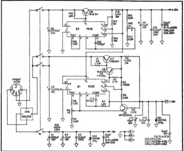
Fig. 16. Power supply circuit.
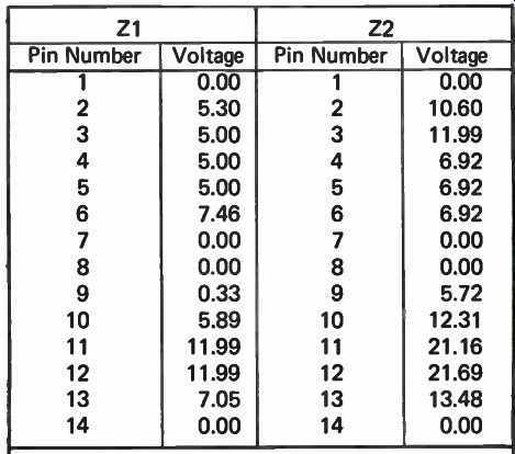
-------------- Fig. 17. Power supply voltage chart.
All voltages are measured with a digital volt meter. Voltages are referenced to ground at the right side of capacitor C9.
----------------
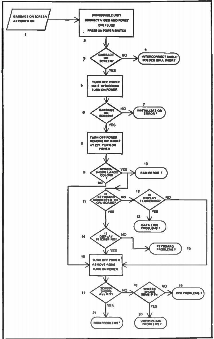
Fig. 18. Part removal isolation flowchart.
Section Isolation Flowchart
Referring to Fig. 18, you will find a flowchart of section isolation "by part removal". Start this process in the parallelogram, block 1, which gives the basic problem. Block 2 instructs you to disassemble the unit and reconnect the video and power inputs. Block 3 is a decision block. Do you have garbage on the screen now? If so, you continue to block 5. If not, block 4 tells you to suspect a shorting interconnect cable between the keyboard and the CPU board. You could also have loosened a "solder ball" during disassembly, and the short is now gone. Examine the interconnect cable carefully for shorting conductors.
Also, note any loose solder or wire bits on the board. You may have solved the computer problem just by taking it apart. So, run another test.
At block 5, you will turn off power to the unit, wait about ten seconds, then switch power back on. The delay gives the initialization logic time to reset. If there is now a "ready" on the screen at block 6, you may have a problem around S2 or C42, as block 7 instructs.
In block 8, you are instructed to remove the dip shunt (X71) at Z71.
Refer to fold out diagrams. With X71 removed, the RAM's are not electronically in the system. When power is applied, the ROM and the CPU are in communication, but there is no data flow to or from the RAM. The screen should show a pattern of 16 character lines of 32 colons. If the CPU shows large colons, you could have RAM or keyboard-type problems. Blocks 11 through 15 will help in isolating that type of problem.
As blocks 12 and 14 imply, there are two colon displays. One display is stable. The other is blinking and flickering as the CPU constantly
interrupts video addressing. Depending on the status of the keyboard, you could have data line or keyboard troubles.
The next step at block 16 is to remove the ROM's. The CPU is now locked up without instructions from ROM. The pattern to look for is a screen full of @ 9's. The display should be in 64 character format at this time. The display will continually be flickering.
If you get@9's on the screen, you probably have a ROM error. If no@ 9's or partial@ 9's are visible, you could have video chain or video RAM problems. If you still get garbage, maybe the CPU is dead or something is making the CPU not function.
As we see, the part removal isolation technique uses a lot of maybe's, question marks and could be's. Teh "what if " are trying to tell us what section could be at fault. You could have ROM problems and yet obtain large colons. You could get @9's and still have CPU error. But it is better than nothing, and the process does give you a starting point.
Signal Condition (Active, Steady State, or Floating)
Normal troubleshooting techniques call for an output-to-input sweep of the bad signal line. Hence, once a bad signal is found, the circuit is traced backwards until the signal is correct. The failed device will be located between the good input and the bad output.
Activity, is defined as any logical transition from high to low or vice versa. For example, the output of oscillator buffer Z42, pin 6, always has activity. There is a constant output pulse train at this pin. The signal swings from almost ground to over 3 volts continuant.
Steady-State. is defined as a logical 1 or logical O. For example, Z40, pin 16, has a steady state logical 1. It is held high by resistor R50. Another example is the logical 0 at pins 6 and 7 of Z56, the CPU clock divider. 142, pin 8, is always low unless resistor R67 is grounded.
Floating, is defined as a signal level between the steady state of a logical 0 and a logical 1. The CPU, the ROM's, the RAM's and the data and address buffers are all tri-stable devices. When tri-state devices are disabled or unselected, the output may show a floating condition. In a floating condition, the output will show system noise flickering through it.
The average level of the noise will attain a voltage of 1.5 volts or so. TTL devices define a logical 0 to be equal to, or less than, 0.8 volts. A logical 1 has a voltage equal to, or more than, 2.4 volts. Any voltage between these two levels will be considered floating.
CPU Problems
A problem with the CPU does not mean that Z40 is inoperative. It could indicate you have trouble with the address and data buffers, the control group, CAS/RAS timing, or with one of the CPU's support devices. If you suspect a problem with these devices, try substitution of a known good CPU for Z40. The flowchart, shown in Fig. 19 will help you for CPU troubleshooting.
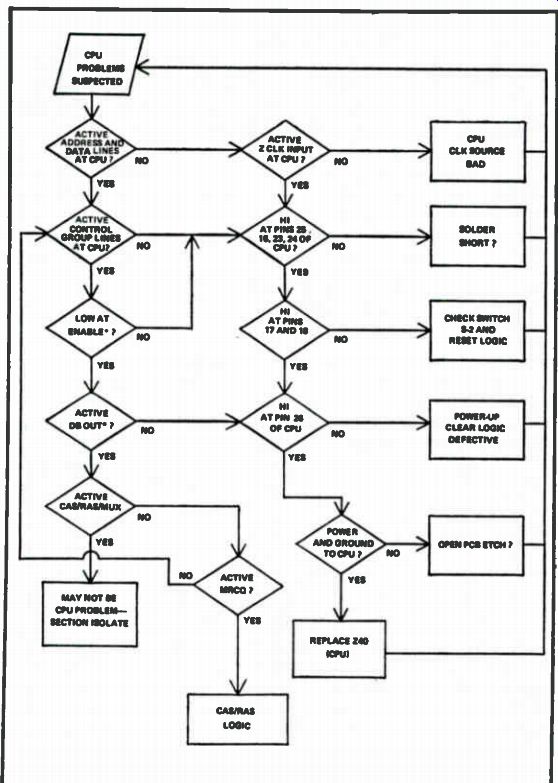
Fig. 19. CPU section isolation flowchart.
The primary objective of this chart is to help you find a signal fast that should be active but is not. The main flow of the chart is on the left side of the blocks. Here, you are checking for activity on address and data lines.
With no activity on the address lines, you are immediately branched off to the CPU's support group to find out why. Pay particular attention to the appearance of address line outputs. Any tri -state looking signal could mean a potential short between address lines. The opposite is true of data lines.
These signals may be active and have floating components between active states. Hence, data line shorts are extremely difficult to find, using an oscilloscope.
Addressing Problems (ROM)
Usually addressing problems are associated with open or shorted address lines going to the ROM sockets. Early versions of the boards may have jumper modifications on the solder side that may have broken loose.
There is also the chance that vibration has jarred a ROM partially out of its socket. The address lines should be checked at the chip. Normally, there will be activity on all lines.
There are two types of data problems. The first one is the non-repairable bit error internal to the ROM. The checksum contained in the SCQATS program can readily verify this. SCQATS is a special machine language test and debugging tape available from Radio Shack for the TRS-80. If the ROM problem is too severe for SCQATS loading, a replacement test may be required. The second type of data problem is the short or open on the data output. If you remove dip shunt Z3, the ROM's will tri -state and you can check for a floating state on the data pins.
RAM Checks
RAM problems are slightly more difficult to troubleshoot because of multiplexing of the address inputs. Aside from addressing differences, the RAM's are checked like the ROM's. If you have a RAM problem and the system will not load SCQATS, you can replace the eight RAM's with a known good set. If this clears the faults, start replacing your standard RAM's with the parts you took out, one by one. Power up after each exchange to see if you still have a "ready". Continue this process until you have isolated the defective RAM (s). Address Decoder Tips A problem in the address decoder section will probably point you in the memory direction. For example, if the ROM is never addressed with ROM, you would think you have ROM problems. If you suspect one of the "memory" locations, keep in mind that the address decoder sources what the memory selects. The select inputs to the different memories should be the very first thing to check out.
Since the address decoder is made up of gates, it should be easy to repair once you locate the fault. The hard part is knowing when to suspect a fault with the decoder section. Section isolation demands that the address decoder be functional, at least partially. Unfortunately there is no "cut and try" way to determine if this section is operating correctly. Of course, you can monitor each output to see if it's responding, but you really can not be sure the signal is supposed to be there when it is.
Keyboard Information
Difficulty with the keyboard is usually mechanical, sticking keycaps, bouncy keys and broken interconnect cables are common. Shorts in the keyboard matrix are usually easy to detect. If you find an alphanumeric character display right after the 7, that particular key, or PCB run, may be shorted. A completely "dead" keyboard could be caused by lack of power, a broken interconnect cable or the address decoder is not feeding a signal to the keyboard.
Video Divider Chain Comments
Problems in the video divider chain will usually be associated with the stability of the display. Loss of vertical or horizontal reference frequencies sometimes can be traced back to defective counters or bad reset gates.
Since the systems master clock/oscillator is included in this section, inactive (dead) system troubleshooting can very well end up at this point.
Since most of the reference and timing signals for the video processor are generated in the divider chain, most (but not all) display difficulties can be isolated to this section. This is especially true of vertical roll or horizontal tear of the display. If the horizontal or vertical reference frequency is not getting to the sync processors, then the problem will definitely be a divider chain foul-up.
Notes on the Video RAM's
If you suspect video RAM problems, you should try a SCQATS tape test loading. SCQATS will be most helpful in rooting out bit-error in the RAM's. If the test generates large amounts of bit-errors, you should suspect either the divider chain or the video RAM addressing multiplexer.
Normally, addressing errors occur when there is a short or open between the multiplexer and the RAM's. Signal activity on the address inputs of the RAM's can be easily checked with an oscilloscope. All address lines (VO through V9) should be active in 64 character format.
There will not normally be any floating conditions on these inputs. The logic input to video RAM will only be active during a NPU data transfer.
Normally, it should be high.
Video Processing
Problems in the video processing section can range anywhere from a blank screen to missing dots. Usually, the fault is easily found because this section is a serial-type. For example, if you have graphics problems, you know there are only two chips that are used as graphics handling devices.
You should then look around shift register Z11 and graphics generator Z.8.
The parts that are strictly alphanumeric are character generator Z29 and its shift register Z10. Defective devices that can affect both alphanumeric and graphics are: Z26, Z27, Z30 and the video mixing circuits, consisting of Q1 and Q2.
Sync Generator Points of Service
The sync generator section is one of the easiest circuits to troubleshoot. If the timing reference is getting to Z6 and Z57, it is a simple process to find the point where you have lost the signal. A problem can occur with the adjust pots, R20 or R21. Severe heat build-up may cause these parts to fail. Capacitors C20 and C26 are usually dependable unless they are physically damaged. You may find C21 or C27 shorted. These capacitors are mylar and are very susceptible to shorting out under impact stress.
An important point about this circuit is that Z6 and Z57 are CMOS devices. Unlike TTL, they are high impedance devices that consume little current. A floating condition on a CMOS input will not necessarily give a floating "display" on an oscilloscope. A floating condition may look high or low depending on the charge of the broken line tied to the input point. Even the resistance of your finger across a broken run can complete the circuit and cause a CMOS device to operate. When you remove your finger from the run or pin, circuit operation may fade away very slowly as the PC board run discharges.
PROCESSOR TECHNOLOGY CORP. SOL-20 MICROCOMPUTER
Some of the special circuits found in the Processor Technology SOL-20 Microcomputer shown in Fig. 20 will now be covered.
Power Supply Circuit
The fused primary power is applied through S5 to T2. Now refer to Fig. 21 for a block diagram of the SOL-20 power supply. A full-wave bridge rectifier, is connected across the 8-volt secondary of the trans former. The rectified output is filtered by C8 and applied to the collector of Q1. Q1, a pass transistor, is driven by Q2, with the two connected as a Darlington pair. The output of Q1 is connected to RI which serves as an overload current.
For the operation of the SOL-20 power supply refer to circuit in Fig. 22. An overload current (approximately 4 amps) increases the voltage drop across R1. The difference is amplified in one-half of U2 (an operational amplifier) and the output on pin 7 turns Q3 on. Q3 in turn "steals" current from Ql-Q2 and diverts current from the output on pin 1 of U2. This in effect turns the supply off to reduce the current and voltage.
Note that the circuit is not a constant current regulator since the current is "folded back" by R6 and R8. The current is reduced to about 1 amp as the output voltage falls to zero.
Divider network R11 and R12, which is returned to - 12 volts, senses changes in the output voltage, If the output voltage is 5 volts, the input to pin 2 of U2 is at zero volts. U2 provides a positive output on pin 1 if pin 3 is more positive than pin 2 and a negative output for the opposite condition.
When the output voltage falls below 5 volts, pin 2 of U2 goes more negative then pin 3. This means pin 1 of U2 goes positive to supply more current to the base of Ql. The resulting increase in current to the load causes the output voltage to rise until it stabilizes at 5 volts. Should the output voltage rise above 5 volts, the circuit operates in a reverse manner to lower the voltage.
Protection against a serious over-voltage condition (more than 6 volts) is also provided. Zener diode, (D1), with a 5.1 Zener voltage, is connected in series with R13 and R2. When the output voltage exceeds about 6 volts, the resulting voltage drop across R2 triggers SCR1 to short the fold-back current to ground. Since the overload current circuit is also working, the current through SCR1 is about 1 amp. Once the current is removed, this circuit restores itself to its normal condition; that is, SCR1 turns off.
Bridge rectifier FWB2, connected across the other T1 secondary, supplies +12 and -12 volts DC. The positive output of FWB2 is filtered by C5 and regulated by IC regulator U1. The negative output is filtered by C4 and regulated by U3. Shunt diodes D3 and D4 protect U1 and U3 against discharge of C6 and C7 when power is turned off. (Note that should the - 12 volt supply short to ground, the +5 volt supply turns off by action of U2). Unregulated - 16 and +16 volt DC, from the filtered outputs of FWB2 are available on terminals X6 and X5. Note the power transformer (T2) has an 8 volt secondary winding and a bridge rectifier (FWB3) to supply +8 volts DC at 8 amps. This output is filtered by C9 and controlled by bleeder resistor R13. The SOL-20 also has a cooling fan powered by AC line voltage.
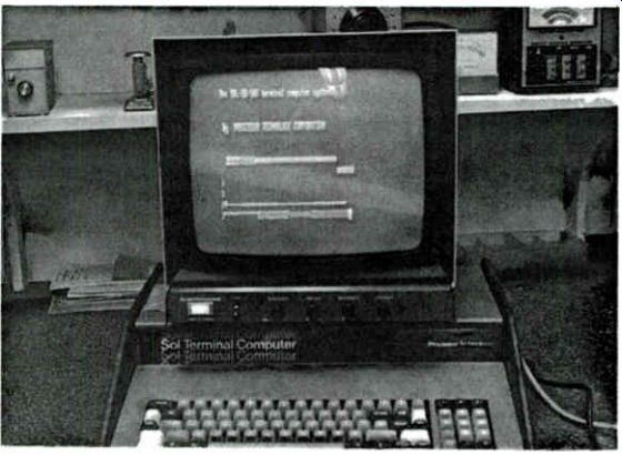
Fig. 20. Photo of SOL-20 computer.
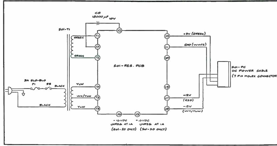
Fig. 21. SOL-10 power supply block diagram.
Audio Tape I/0- Sol-20 System Refer to audio tape I/O schematic Fig. 23. Timing for the audio tape I/O is derived from the 1200, 2400, 4800, 19,200, and 38,000 Hz signals received from the Baud rate generator in the input/output section of the SOL. The first two are used by the write data synchronizer (U100) and the digital-to-audio converter (U101). The remaining three signals are fed to two sections of U111, a quad multiplexer or select gate. All four sections of U111 are used to select clocks for low speed or high speed operation according to the select inputs, pins 9 (A) and 14 (B). The states of these two select inputs must be complementary to each other in order to select the high or low speed clocks. Specifically, A must be high and B low to select high speed clocks; the reverse condition selects the low speed clocks mode.
The output of the second section on pin 11 of U111 is BYTE write clock, 4800 Hz on low speed and 19.2 kHz on high speed. The third section outputs a 19.2 kHz (high speed) or 38.4 kHz (low speed) timing signal to input pin 10 of binary up counter (U112). Recover clock is produced by a phase locked loop (U111), another U112 binary up counter and the first and fourth sections of U111. The signal input (pin 14) to U110 is supplied from output pin 1 of D flip-flop U113. It is a constant frequency, regardless of whether one or two transitions are detected in the read data during the count out time (12 counts) of the U112 counter with the outputs on pins 13 and 14. A phase comparator in U110 compares the signal input to the output of a voltage controlled oscillator (VCO) in U110 (pin 4). By feeding the VCO output through a counter (the other half of U112) before feeding the counter output back to the compare input (pin 3) of U110, the circuit acts as a frequency multiplier. The output of this circuit remains locked, therefore, to a multiple of the signal input on pin 14 of the U110 chip.
The output of U110 is nominally 19.2 kHz. The actual output is determined by the signal input which in turn is a function of tape speed. In other words, the phase lock loop circuit tracks input frequency variations.
And it will track such variations within its locking range which is determined by the setting of variable resistor VR3 (connected to pin 12 of the U110 chip). For high speed, the divide-by-four output of U112 (pin 4) is selected as recover clock. For low speed, the VCO output of U110 is selected for recover clock. This clock serves as read clock for the CDI UART, U69.
Tape control 1 and 2 are used to turn one or two recorder motors on and off. An active low tape control 1 energizes KI to close its contacts and turn recorder 1 on; a high de-energizes KI to turn the recorder off. Tape control 2 does the same thing with K2 to control another recorder. Diodes D13 and D14, which shunt K1 and K2 respectively, prevent damage to the logic circuitry in the input/output section due to inductive kickback. R155 and R156 are current limiters that keep the relay contacts from being "welded" together.
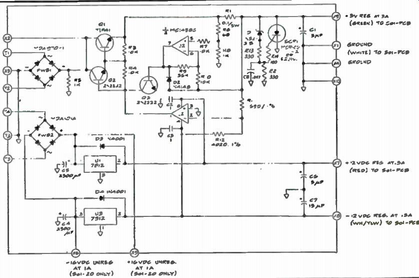
Fig. 22. Circuit diagram for SOL-20 power supply.
When the CD1 is in the write mode, data is input to the UART (U69)
under control of port out FB. Upon completion of this strobe, the transmit sequence is initiated within the UART, with the transmission rate being governed by the BYTE write clock.
The transmission sequence begins with a start bit, a low (data zero) on the UART's TO output. It is followed by eight data bits and two stop bits (high on the UART's TO output), with the number of bits being fixed by the connections to pins 34 through 39 of U69.
The data from U69 is applied to the D input of D flip-flop U100 which is clocked at 1200 Hz. This output is connected to the reset (pin 4) of the U101, so when the data out of the UART is high, the first section in U101 is forced to a reset condition. In this condition the J and K inputs to the second stage of U101 are held high which allows the flip-flop to change state on the rising edge of the clock.
The clock for U101 (OUTPUT CLOCK) is 2400 Hz in the high speed mode or 4800 Hz in the low speed mode. This clock is derived from 2400 Hz in conjunction with the low speed select signal in NAND gate U98 and exclusive OR gate U99.
In the high speed mode, pins 12 and 13 of U98 are held low, thus holding pin 10 of U98 high. As a result, the 2400 Hz signal is inverted in U99 to become the clock for U101.
Pins 12 and 13 of U98 are held high, however, in the low speed mode to enable U98. In this case R117 and C47 provide a delay in the U98 gate.
When the 2400 Hz signal on pin 2 of U99 changes state, so does pin 3 of U99. Also, C47 charges through R117 for several g sec, at which point pin 10 of U98 is brought to the opposite polarity. The output from U99 then goes high. A series of positive pulses, with a pulse width approximately equal to the R117, C47 time constant (10g sec) and occurring at every transition of the 2400 Hz signal, appears on pin 3 of U99. This circuit thus operates as a frequency doubler in the low speed mode to provide a 4800 Hz clock for U101.
The 2400 Hz signal from which the U101 clocks are derived also produces the 1200 Hz clock signal for U100. As a result the 1200 Hz signal changes state following a propagation delay after the 2400 Hz signal falls.
Output Clock
As previously stated the second stage of U101 is allowed to change state on the positive going transitions of the output clock as long as the data out of the synchronizer is a "1". The end result is an output on pin 14 of U101 that is one-half the clock frequency (1200 Hz and 2400 Hz in the high and low speed modes respectively). Assume the data stream out of the UART goes low (0). On the next rising edge of the 1200 Hz signal, U100 will reset with Q low and Q high. A low reset on pin 4 of U101 enables the first U101 stage to toggle on the next rising edge of the output clock which occurs 1/2400 second after the synchronizer output falls. Remember that output clock moves from a low to a high shortly before the 1200 Hz signal. The reset on pin four of U101 is thus removed slightly after the output clock occurred. With the J and K inputs to the first U101 stage high, its output will change state on each succeeding low to high transition of the output clock. The second U101 stage in turn can only toggle on the positive going transition of the output clock when its J and K inputs are high. Since the inputs are high at one-half the clock rate, by virtue of the first U101 stage, the second U101 stage toggles at one-fourth the output clock rate.
The two sections of U101, therefore, operate as a frequency divider, dividing the output clock by two when the write data is a "1" and by four when the data is a "0". Thus, in the low speed mode, four cycles of the 1200 Hz represent a "0" and eight cycles of 2400 Hz represent a "1". In the high speed mode, one cycle of 1200 Hz represents a "1" and one-half cycle of 600 represents a "0". The output on pin 14 of U101 is applied to one section in U109 which provides sufficient current drive for the divider network. This divider and a jumper arrangement allow selecting one of three outputs to be fed to the audio output jack J6. The I to J jumper selects a 500 mv signal for the auxiliary input to an audio recorder. The I to H jumper selects a 50 mv signal for the microphone input to an audio recorder.
When the CD1is in the read mode, data from the recorders enters on J7. This input is fed to the negative input (pin 6) of the operational amplifier U108.
The first section of U108 is a high gain amplifier, with its gain (approximately 100) being determined by R142 and R143. The output from this amplifier is coupled to input pin 2 of the following U108 stage and the base of a Darlington pair (Q4 and Q5) which provides high current gain.
Current into the base of transistor Q5 causes C67 discharge (C67 charges through R39 to 5 volt DC). The voltage on C67 in turn controls the gate of field effect transistor (FED Q3. Q3 functions as a variable resistor which can be changed by its gate voltage. Since Q3 is connected between ground and the input network to the first U108 stage, it serves as a variable shunt. A low gate voltage on Q3 decreases the shunt resistance and the input to U108. In a like manner, a high voltage on C67 results in an increased input to U108. Q3, Q4, and Q5 with their associated circuitry, therefore, serve as an automatic gain control (AGC) circuit which limits the input to the second U108 stage to approximately a positive 2 volts peak signal.
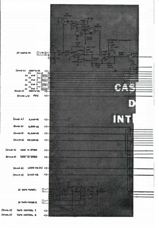
Fig. 23. Cassette data tape interface diagram for SOL-20 microprocessor
computer.
The second stage of U108 is a comparator with hysteresis that performs the needed audio to digital conversion. Feedback resistor R147, in conjunction with R145, establishes the level on the positive input (pin 3) of U108. This level, be it positive or negative, is the threshold voltage, ± 50 mv, which the negative input (pin 2) must exceed in order for the output of U108 to switch levels, positive to negative and the converse.
Since the feedback loop is regenerative, U108 switches at its maximum rate, and U108 switches on each transition of the audio signal input. It is in this manner that U108 performs the audio to digital conversion.
The digital output of the U108 is inverted in one section of inverter U109 and applied to pin 9 of exclusive OR gate U99 which is connected as a buffer without inversion, li the output of U109 is low, the output on pin 10 of U99 is also low and the output on pin 4 of another U99 exclusive OR gate is high. The voltage across C49 under this condition is minimal. When the output of U109 goes high, C49 starts to charge through R118 until pin 9 of U99 crosses the threshold of that gate. At this point pin 10 of U99 goes high, and since the two inputs to the second exclusive OR gate are both high, pin 4 of U99 goes low. C49 now discharges because pins 9 and 10 of U99 are at the same level so that the circuit can repeat the operation on the next high to low transition at pin 4 of U109. R118, C49 and U99 consequently serve as a transition of the output on pin 4 of U109, regardless of the polarity of the transition.
Transition pulses from the U99 clock go to both D flip-flops in U113.
A transition pulse clocks the top U113 at pin 3 which sets Q (pin 1) high and Q (pin 2) low to enable up binary counter U112 on pin 15. Pin 1 is applied to the D input (pin 9) of the lower U113 and the circuit remains in this state until one of two things occurs: a second transition pulse arrives before U112 reaches count 12 or U112 reaches count 12.
If a second transition pulse arrives before count 12, the bottom U113 stage is set and presents a "1" to the D input (pin 9) of flip-flop U100. This is clocked by the Q output on pin 2 of U113 as a low to pin 12 of U100. If a transition pulse does not arrive before count 12, the bottom U113 stage outputs a "0" to input pin 9 of U100. On count 12, the C and D outputs of U112 go high to reset U113 by way of U98 at pin 4. As a result the U100 clock goes high, as does pin 12 of U100. The output on pin 12 of U100 is inverted by U109 and applied to the receive input (pin 20) of the UART. The Q output on pin 1 of U113, which occurs at the actual bit rate of the incoming data, is also used by the receive clock circuitry to reconstruct the receive clock from the data signal.
Received data undergoes serial-to-parallel conversion in the UART and is placed on the R01-8 data outputs of the UART when ROD (pin 4 of the UART) is low (port in FB active) and onto INTO-7.
Four status outputs from the UART can also be enabled when SFD (pin 16) is low. These four bits are FE (framing error), OE (overrun error), DR (data ready) and TBRE (transmitter buffer register empty).