Knowledge of the internal construction and chemistry of a transistor is not necessary for efficient troubleshooting. But it is very helpful to take the basic physical construction of a typical transistor (Fig. 1A) and visualize it as two diodes wired back-to-back as shown in Fig. 1B. Of course, two separate diodes cannot possibly have collector-emitter current and thus cannot amplify.
In an actual transistor, the two diode junctions are seldom symmetrical and the base material is so thin that current can flow through it between collector and emitter when stimulated by collector voltage and a forward base bias. Varying the base bias by a signal causes collector current variation; this is amplification.
According to the way a transistor measures on an ohmmeter, its "black box" circuit consists of three diodes and two resistors, as shown in Fig. 2A. The chart in Fig. 2B is a good guide to the approximate readings expected with germanium transistors when checked on a VTVM has a 1.5 volt ohmmeter battery. Don't be surprised if many normal transistors show more base emitter than base-collector leakage.
This only means the collector and emitter are not symmetrical. If you use other scales, or a meter with another battery voltage, the resistance readings will be radically different, since all solid-state diodes change resistance according to the voltage applied to them.
The same low base-emitter, base, collector or collector-emitter ohm meter reading when the test lead polarity is reversed, indicates a defective transistor with a shorted junction. An open reading for both polarities indicates an open junction. One common defect is a short from collector to emitter. Often there is no corresponding short from the base to either the collector or emitter. This is difficult to under stand since the base is located between them. Evidently the excessive current caused by the collector-emitter short burns away the base material around the shorted area.
Silicon power transistors also can be checked as shown in the chart of Fig. 2B, although all the resistances will be much higher than those listed. Tests of small silicon transistors will be limited since the leak age resistance will be above the highest ohmmeter scale. During checks on both germanium and silicon transistors, don't use a lower scale than the Cones specified in the chart for forward bias readings because the ohmmeter current (which reaches 150 mills on the X1 scale) might damage small transistors.
You may question why we should bother to check transistors with an ohmmeter when there are many excellent transistor testers on the market. First, there are many more ohmmeters than transistor testers around a typical workbench. But more important, the ohmmeter tests give more of an insight into circuit voltage and resistance measurements and how they are affected by transistor defects. It is excellent belt and-suspenders technique to use ohmmeter readings to verify the verdicts of the transistor tester.
Tubes vs. Transistors
After the obvious lack of a heater in a transistor and the necessity for a high vacuum surrounding the elements of a tube, the next radical difference between tubes and transistors is in the polarity of the bias and the elements (Fig. 3.) A tube without bias (grid shorted to cathode) will draw excessive plate current. A transistor without bias (base shorted to emitter) will have a minimum collector current, and making the base positive increases he collector current. The tube plate voltage is positive, the polarity to cause maximum conduction, while the grid is negative to prevent any grid current.
By contrast, the positive voltage applied to the transistor collector will cause less collector current than would a negative supply (but this current would not be under the control of the base-emitter). The base is positive which is the polarity to cause maximum base current. A negative base voltage would be re verse-biased and would result in no base or collector current (except leakage). To say these facts another way, a grid is reverse-biased, a plate is forward-biased, a base is forward biased and a collector is reverse biased. A transistor always draws base current (low impedance input) and a tube has no grid current (high impedance input) when both are operated in class "A". Effects of Heat Current and gain in vacuum tubes are affected very little by ambient temperature since each tube has its own private built-in furnace that is many times hotter than the surroundings. Not so with transistors. Heat is not necessary for normal operation; any generated heat is strictly a byproduct, and often a detrimental one.
Those of you who have experience only with well-designed solid state circuits may be surprised how thermally unstable some of the simpler circuits can be. In the low-level audio circuit of Fig. 1A, assume that the base resistor is the correct value to produce maximum gain.
Use an audio oscillator for an input signal, monitor the output with an AC meter and the collector with a DC meter. Just cup your thumb and forefinger around the transistor case for a few seconds and watch both the output AC and collector DC voltages drop enough for a definite difference in reading. If you go one more step and also monitor the base-emitter voltage, you will discover that the base voltage de creased from this slight increase in heat. The transistor conducted more collector current with less base voltage. Or turn that statement around, so it reads: for the same collector current, less forward bias is required at higher temperatures.
It is undoubtedly true that more base current caused more ,collector current (transistors arc "current amplifiers"), but base current is very difficult to measure, while base voltage measurement is simple if you have a meter with a full-scale reading of .5 or 1.0 volt. Later we will show that collector or emitter current can be measured easily by reading a resistance, the voltage drop across it and calculating the current by Ohms Law.
Stabilization
Four basic types of temperature stabilization are commonly used.
Fig. 4B shows the base voltage sup ply taken from the collector rather than the supply voltage. This is an effective method, if the resistance in the collector circuit is fairly high.
Any increase in collector current will lower the collector voltage which in turn reduces the base sup ply voltage. And this lower base voltage will decrease the collector current. The opposite action takes place if the collector current goes down.
There are two limitations. Transformer output coupling is not practical since the collector DC voltage would not change enough for effective control, and the resistor between collector and base can intro duce negative feedback which lowers the gain.
The two most common thermal stabilizing methods are both shown in Fig. 4C. Forward bias for the base is developed by a voltage divider to minimize voltage variations, and more important, an emitter resistor is added. For example, increased emitter current raises the emitter-to-ground voltage and any emitter voltage is subtracted from the base-to-ground voltage to give the true forward bias. The more emitter voltage, the less forward bias and this causes less gain and collector current.
Let's consider some hypothetical voltages. Assume a base-to-ground voltage of -2.15 and an emitter-to ground voltage of -2.0; the forward bias is -.15 volt. Suppose that a higher transistor temperature increases the collector-emitter current so the readings become: base -2.15, and emitter -2.05 for a forward bias of -.10. This reduced forward bias decreases the collector-emitter current and restores the change in gain. Of course, reverse action takes place if the emitter current goes down, but we are not so concerned because this is just the opposite of "thermal runaway". Omission of the emitter bypass capacitor would allow AC current feedback which reduces gain just as an open cathode capacitor will do in tube circuits. In practice, however, we find the gain reduction in transistor circuits to be much larger than that caused in tube circuits by an open capacitor, where the resistor is the same in both cases. In a tube circuit, the gain might be reduced 10 dB, while the transistor circuit gain could be decreased by 20 to 30 dB. The fourth type of heat stabilization uses a diode (of the same material as the transistor) as a voltage regulator.
How Critical is Forward Bias?
. The forward bias of a transistor
--------------------- BASE COLLECTOR
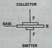
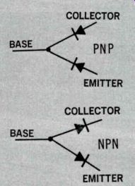
Fig. 1A PNP transistors have a thin section of "N" material between the "P" sections. NPN types are reversed.
Fig. 1B Each junction of “P" and "N" material has diode properties. For resistance tests they can be diagramed as di odes.
-----------------
... is the most critical factor that determines the performance of transistorized circuits. Without some forward bias, there can be no collector current (except undesired leakage), and since a small transistor typically operates with about 0.2 volts of forward bias for a germanium type and about .7 volts for a silicon, small voltage changes are significant merely because the bias is small. Logic and reason tell us that a 10% change in forward bias should have the same effect on gain and output current as a 10% change in tube bias. This is not so! In some transistor circuits a bias change of far less than 10% can increase or decrease the gain 30 dB, for example. This is far more critical than the bias on a high-gain sharp-cutoff tube.
It is poor design and practice to apply a fixed bias even from a well regulated supply, for the optimum bias will be different for each individual transistor and will vary widely according to the junction temperature. For stages such as power output that are difficult to stabilize, a bias-regulating diode may be used if it is made from the same type of material as the transistor so it will have a similar temperature coefficient. Even applying a constant base current is not enough stabilization. If it were, a large source of voltage through a large base resistor would be sufficient. Two methods of stabilizing a single stage were given previously.
One is to use a large emitter resistor, and the other is to take the bias from a source (such as the collector) that varies in voltage according to collector current. Later we will explore how multiple direct coupled stages ere stabilized.
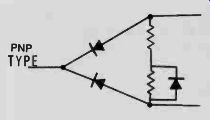
Fig. 2 This is the equivalent of a transistor when it is measured by an ohmmeter.
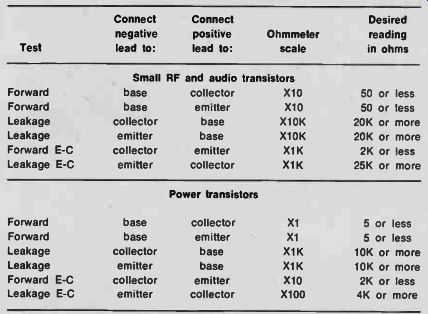
Fig. 2B Chart for measuring the junction resistances of PNP germanium transistors.
All polarities should be reversed to test NPN types. These readings are for
VTVM's using a 1.5 volt ohmmeter battery. Meters with other battery voltages
will show different resistances.
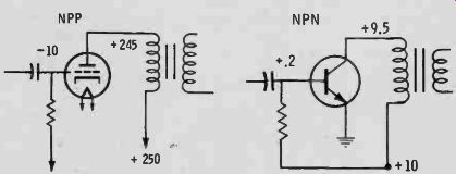
Fig. 3A Any tube could be called an NPP type since both grid and plate will
pass current if they are positive in relation to the cathode.
In practice, a tube is operated with a reverse-biased grid and forward biased plate.

Fig. 3B Transistors are operated with the base (grid) forward-biased, and
the collector (plate) reverse-biased.
Forward-biased elements are low impedance and reverse-biased elements present a high impedance.
Gain Control by Bias Variation
Every transistor has an optimum forward bias that gives maximum gain. Either more or less bias de creases the gain. There is no precedent in tube circuitry for this characteristic. The graph in Fig. 5 is not intended to be accurate, but only to illustrate general transistor functions. The forward bias is increased at a linear voltage rate.
The collector current increases and the input impedance decreases at a logarithmic rate, while the gain peaks at one definite bias voltage.
Starting at the bias for maximum gain, a decrease in bias uses the "cut-off" mode, and in increase takes advantage of the "saturation" characteristic for gain reduction.
Either method can be made to give about the same degree of gain reduction. Current consumption would dictate use of the cut-off type of AVC for battery-operated equipment such as portable radios. AGC in television receivers usually em ploys the saturation method, for the lower input impedance obtained on stronger signals widens the band width of the tuned circuits.
Silicon transistors used for IF and RF amplifiers in color TV receivers appear to have an extremely sharp cut-off when saturation biasing is used for AGC. Actual measurements made on several brands of receivers indicate that a bias increase of only .04 to .05 volts over the no-signal bias of about .7 volts will accomplish adequate gain reduction for a very strong TV signal. Translated, this means a bias increase of 7% will reduce the gain to virtually zero.
Pulsed Signal Operation
The preceding statements apply to AF, RF and IF amplifiers operated in class "A". Class "C" amplifiers (including oscillators, sync separators and power output stages) usually show reversed bias measured on a meter. This does not contradict facts on forward bias already given.
Diode action of the base-emitter junction rectifies the incoming signal to produce reversed bias that …
-----------------
Fig. 4A Simple audio amplifier with out thermal stabilization.
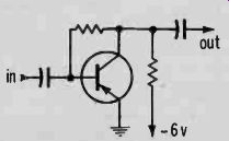
Fig. 4B Effective stabilization for resistance-coupled circuits.
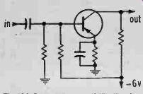
Fig. 4C Base voltage stabilization by a voltage divider. The emitter resistor
helps thermal stabilization the most of the two methods.
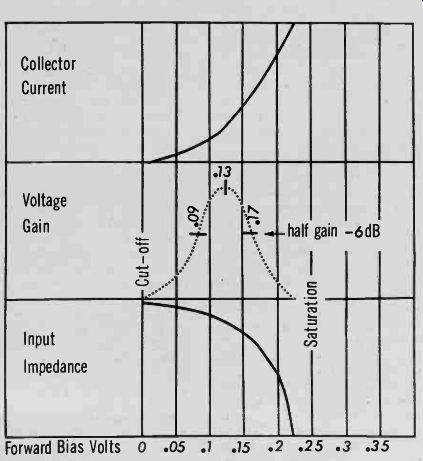
Fig. 5 Characteristics of transistor.
---------------------
…is overpowered by the highest amplitude tip of the incoming wave form to become forward bias. Thus the base has reversed bias most of the time, and forward bias for a very short time during each cycle.
A meter will average these voltages to read as reversed bias.
Load Impedance vs Gain
Load impedance in the collector circuit has a large effect on transistor gain. At the usual transistor impedances (under 50,000 ohms) the gain is in direct proportion to the load. If the collector load impedance is doubled, so is the gain (+6 dB). If the impedance is decreased 20%, the gain is reduced 20%. Remember this when analyzing some of the beginner circuits where the collector resistor is about 1.5K.
Other Factors Affecting Gain
Collector voltage is not a critical factor in determining gain except when the collector-emitter voltage drops to a few tenths of a volt, then the gain drops to nearly zero.
Negative feedback or degeneration in the emitter circuit from un bypassed resistors reduce. gain with transistors the same as it does in tube equipment.