by Bruce Anderson
The precise manner in which a transistor operates may be of interest and value to some; however, those of us engaged daily in repairing transistorized equipment can perform our task with considerably less information. Nevertheless, a few of the characteristics of a transistor must be remembered. These essential bits of information are summarized as follows:
1. The average amount of DC voltage present between base and emitter remains nearly constant, so long as the transistor is in a state of conduction. Obviously, if the base voltage is insufficient to allow emitter-to-base conduction, the potential between these two elements may vary; but if there is normal conduction, the voltage will remain al most constant. This is quite different from a tube, in which the grid voltage may vary over a fairly large range, perhaps 10 or 15 volts, during normal operation. Conversely, the grid current is very small (and nearly constant) throughout the operating range, while base current is significant and variable.
2. Since the base voltage remains nearly constant throughout the normal range of operation, the input impedance of the device itself is inversely proportional to the input signal level. The input impedance may be increased by connecting an unbypassed resistance in series with the emitter of the transistor. This raises the overall impedance seen at the base and tends to make it independent of the signal level.
3. Unlike a tube, whose input impedance is normally in the order of thousands or millions of ohms, the input impedance of a transistor connected in a common-emitter circuit is quite low. As a general rule, it may be estimated by multiplying the impedance between the emitter and ground times the beta of the transistor. Thus, if the transistor shown in Fig. 1 has a beta of. 100, the input impedance probably will be about 1000 ohms. Any biasing resistors in the base circuit will be shunted across this input impedance. This resistive component of the impedance might be shunted by a fairly low value of capacitive reactance, which will lower the impedance further. Naturally, if the emitter resistor is bypassed, the capacitive reactance "seen" at the base will approximate the reactance of the capacitor multiplied by the beta. To calculate this impedance, the frequency of operation has to be known.
4. Since the amount of collector current is determined by the emitter-to-base current to a much greater degree than it is determined by the collector voltage, the collector load impedance of a common emitter transistor circuit can be quite high.
5. If the emitter-to-base current is made high, driving the device into saturation, the voltage drop from emitter to collector may be come almost negligible. This is un like a tube, in which the cathode to-anode drop is considerable, even when the control-grid voltage is positive with respect to the cathode.
6. Transistors are available in either of two types, NPN and PNP. This allows operation with the collector supply either positive (NPN) or negative (PNP). This allows greater latitude in the design of complete circuits, by using stages of different types. In the discussion here, NPN devices are considered.
If a PNP device is encountered in a circuit, the operation will be about the same, except that all polarities are reversed.
7. Unlike a tube, the characteristics of a transistor are not as likely to change over long periods of time.
A tube gradually wears out, from the time it is placed in operation.
On the other hand, a transistor which has been in service for an extended period is likely to produce just as much gain as it did when first installed. Tubes usually fail because they no longer can produce gain; transistors usually fail because of shorts, opens or leakage.
8. Also unlike a tube, the characteristics of a transistor vary considerably with temperature. This can lead to a condition called "run away," wherein an increase in temperature causes an increase in current, which causes an increase in temperature, etc., until the device is destroyed. This is primarily a de sign problem, but it may be the result of circuit malfunction. Also, it makes it doubly important not to obstruct the normal circulation of air inside the cabinet of transistor equipment.
9. The beta of a transistor, which is directly related to the amount of gain possible in a transistor-equipped circuit, is not held to tolerances which are as stringent as the transconductance tolerances of tubes.
Since the beta of each of a number of transistors of the same designation may vary considerably at the time of manufacture, and since these values of beta are not apt to change very much throughout the life of the transistors, the measuring of beta is not a particularly exact test of a suspected transistor.
This, however, does not discourage the use of a beta-type transistor tester, which provides a convenient means of testing for shorts, opens and leakage.
In the light of the above characteristics, it is possible to predict the manner in which certain malfunctions of the surrounding circuit may affect the operation of the transistor and the circuit.
The effect of a change in the value of each of the components in Fig. 2 can be studied, and, by extension, these may be used to predict the operation of similar circuits.
Changes in R1
The value of R1 can increase or decrease; this change may be rather slight, perhaps 20%, or it may be drastic, such as a complete short or open.
Suppose that the resistor were to increase moderately in value. If this should happen, the voltage drop across it would increase and the drop across R2 would have to de crease. (Since the bleeder current through R1 and R2 is much greater than the base current of the transistor, which also passes through R1, this latter current may be ignored for simple calculations.) As the drop across R1 increases, the bias voltage on the base of the transistor must decrease; but as the base voltage and current decrease, the emitter and collector currents of the transistor also will decrease, reducing the emitter voltage.
The result of this moderate increase in the value of R1 is a reduction of the base and emitter voltages of the transistor, and because the collector current has been diminished, the collector voltage will increase. These would be the most obvious symptoms observed with a meter.
Most transistors used in audio applications are biased at a point where an increase in emitter-to-base current will increase the gain of the stage (if it has any effect at all), so a moderate decrease in the base current also might decrease the gain moderately.
Suppose that the value of R1 should increase drastically, perhaps to 100K ohms. With so much resistance between B+ and the transistor base, the base voltage is forced below the barrier potential of about .7 volt. This, of course, will cause the transistor to cut off, dropping the emitter voltage to zero and causing the collector voltage to increase to nearly 13 volts.
Before proceeding, there is an important exception to the usual rule that gain increases as the emitter-to-base current of an NPN transistor is increased. In the IF-amplifier circuits of many television receivers, the transistors are biased so that an increase in emitter-to-base current causes a decrease in amplification, even though the collector current does increase. This is called "forward AGC", and can cause a lot of confusion to the unwary.
(Dale's Service Bench in this issue explains forward AGC.) Now consider the results if R1 decreases in value. According to Ohm's law, the base voltage must increase, increasing the emitter-to base current. The emitter voltage rises right along with the base voltage (discounting a couple of milli volts), and the collector voltage falls because of the additional current through R4. As the value of R1 continues to decrease, the base and emitter voltages will continue to rise, and the collector voltage will continue to fall until they are all about the same, or until the transistor burns out from excessive base current.
Regarding the burnout problem, this is sometimes difficult to predict.
In the circuit shown, the emitter resistor will limit base current to about 18 ma, even if R1 is shorted.
Some transistors will withstand this overload; others will not. Nevertheless, the circuit shown does provide some protection to the transistor.
If the value of R3 were only 3 or 4 ohms, it is almost a certainty that shorting R1 would burn out the transistor. For more information on transistor overloads and burnouts, refer to ELECTRONIC SERVICING, November, 1969, pages 26 to 28.
Changes in R2
To some degree, the effects of changes in the value of R2 will be opposite those caused by changes in R1; however, there are some exceptions. If the resistance of R2 de creases, there will be a reduction in base voltage and emitter-to-base current, and if the change is sufficient, the transistor will cut off.
If the value of R2 increases, base voltage will increase; but even if R2 should open, the base current will not "go through the roof." Since ...
-----------------------
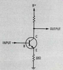
Fig. 1 Basic common-emitter circuit.
---------------------
... the base current causes a drop across R1, the base current cannot exceed that value which will drop all the supply voltage across R1.
About 2 ma will drop 13 volts across R1, and the base current will be even less than this, since there is some drop across R3. Perhaps 1 ma is a reasonable "guesstimate" of the maximum base current possible if R2 is open. It is apparent that the transistor is less apt to be damaged by opening R2 than by shorting R1. Changes in R3 An open cathode resistor in a vacuum-tube circuit will cause the cathode voltage to rise almost to B+, but the effect of opening the emitter resistor (R3 in Fig. 2) in a transistor circuit is not the same.
If the transistor base was disconnected from the junction of R2 and R1, the voltage at this point would increase to about 3.7 volts. With the transistor again connected back in the circuit, it cannot conduct if its emitter rises above about 3 volts, so the emitter voltage normally will never increase above this level, regardless of how large R3 becomes.
The decreased conduction will cause the voltage at the collector to rise, but probably not much. A large increase in the emitter resistance in Fig. 2 might increase the emitter voltage to nearly 3 volts.
This leaves about 10 volts to be dropped across the transistor itself and the collector load-not much change from normal conditions. The most obvious symptom would be a loss in amplification.
Decreasing the emitter resistance tends to decrease the emitter voltage, but this, in turn, increases the base and collector currents. The result is that there will be a sag in the base and emitter voltages, but it will not be in proportion to the reduction in emitter resistance. For example, a 25% reduction in emitter resistance might cause a reduction in emitter voltage of only 10%. However, the emitter current would increase significantly, reducing the collector voltage, and there is a good possibility that the current ratings of the transistor would be exceeded.
Changes in R4 The collector current of a transistor is fairly independent- of the collector voltage, much the same as in a tube. A loss of 25% of the collector resistance of Fig. 2 would cause a corresponding decrease of 25% of the drop across R4, and the collector voltage would increase to about 11 volts. However, this might be rather difficult to detect with a meter having only 5% accuracy.
For his reason, it is wiser to measure the voltage across the resistor instead of the voltage from collector to ground.
If the collector-load resistance changes, it will have very little effect on the voltages at the emitter and the base. And this is the tip-off--if the collector voltage is wrong, but the base and emitter voltages are right, look at the collector-load resistor. Of course, if the resistor is off by 200 percent, this rule may not hold.
If the collector load resistance is off tolerance, the gain will be changed by the amount of tolerance shift, since gain is more or less proportional to load resistance. Of course, this cannot go on without limit if the resistance increases-the amplitude of the output signal can not exceed the collector supply voltage. Also, the transistor might go into saturation or cutoff if the collector resistance is out of tolerance, This will cause distortion.
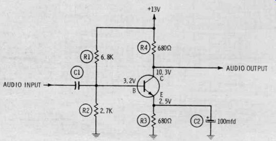
Fig. 2 Typical common-emitter audio amplifier.
Fig. 3 Basic emitter follower.
Changes in C1 If the value of the input coupling capacitor is not within tolerance, there can be an increase in distortion of low-frequency signals, and if the capacitance loss is sufficient, the gain of the amplifier will be de creased seriously. Finding this particular trouble is a job for the scope or perhaps even more practical, a quick job of bridging the capacitor with a new one.
If the coupling capacitor becomes leaky, the result is about the same as decreasing the value of R1. The emitter and base voltages will rise, and the collector voltage will drop.
If there is enough leakage to drive the transistor near saturation, distortion will be produced; more leakage probably will destroy the transistor.
Changes in C2 The function of C2 in Fig. 2 is analogous to the function of a cathode bypass of a tube-circuit. If it loses its capacitance, degeneration of the signal will result (the emitter voltage will vary with the AC signal). If C2 becomes leaky, the result is about the same as if the resistance of R3 had been decreased.
Common-Collector Circuits
The common-collector circuit shown in Fig. 3, also called an emitter follower, is encountered quite often in solid-state circuitry.
Essentially, it is an isolating stage used to match the impedance of the preceding stage, or the input to the instrument, to some lower-impedance load. This may be the next amplifier stage, or perhaps the load to which the instrument is connected. The input impedance may be very high, as in some solid-state electronic volt-meters, if the value of R3 is made sufficiently large. As with the common-emitter amplifier, the input impedance is approximately the value of unbypassed emitter resistance times the beta of the transistor.
One important fact about an emitter follower is that the voltage gain can never be greater than unity (1).
If the input signal has an amplitude of 1 volt, the output must be less than 1 volt. On the other hand, the power gain of an emitter follower may be fairly high. For example, assume that R3 is 100 ohms and that R1 and R2 each have resistances of several thousand ohms.
If the transistor beta is 50 and the input signal is 1 volt, the input impedance is about 5K ohms, and the driving power is about 0.2 milliwatts.
An output signal of .9 volt is entirely possible under these conditions, and this signal is developed across R3, 100 ohms. Therefore, the power output is 8.1 milliwatts, and the power gain is about 40. When troubleshooting an emitter follower, it is important to remember that fairly large variations in the values of the components might not cause the circuit to become completely inoperative. An increase or decrease in base bias, caused by a change in R1 or R2 in Fig. 3, will cause a corresponding change in the emitter voltage, but the gain of the circuit may not be affected notice ably. It is more likely that the new bias levels will cause the transistor either to cut off or saturate during some part of the cycle of the input signal, in which case distortion will occur.
----------------------
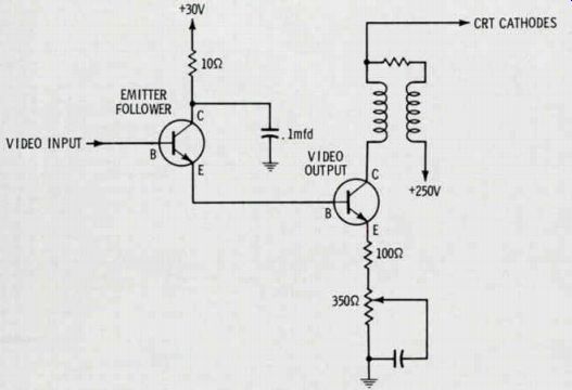
Fig. 4 Direct-coupled emitter follower and video amplifier.
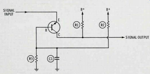
Fig. 5 Typical common-base amplifier.
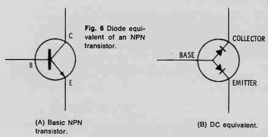
Fig. 6 Diode equivalent of an NPN transistor.
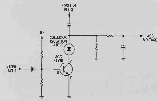
Fig. 7 Diode used for collector isolation.
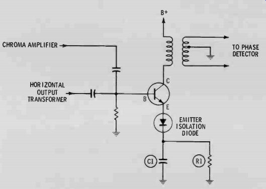
Fig. 8 Diode used for emitter isolation.
-----------------------
R4 in this circuit may be omitted if the supply voltage is correct for the transistor being used. If this is the case, the collector voltage is not likely to change, regardless of the condition of the circuit. When the collector is connected directly to B+, the transistor is very vulnerable to burnout if the emitter resistance becomes too small.
In many applications, the emitter resistance actually is the base circuit of the next stage, as shown in Fig. 4. Characteristically, if the output stage shorts, placing B+ on the emitter of the emitter follower, the emitter follower also will be damaged. Even if the device does not fail immediately, it can after a few hours of operation, and it sometimes is smart to replace it while the set is on the bench.
Again referring to the circuit in Fig. 4, a word of caution is in order: It is common practice to short together the emitter and base of a transistor to check it for leakage. In this circuit, if the base and emitter of the video-output stage are shorted together, the emitter resistance of the emitter follower will be reduced severely, and it is very possible that the transistor will burn out.
Common-Base Circuits
The third configuration of a transistor amplifier is the common-base circuit. Like the common-emitter circuit, it has voltage gain, but the input impedance always is very low.
The common-base circuit may be used to follow some low-impedance source, such as a video delay line, or as the voltage amplifier for a cascode amplifier or mixer. The output impedance can be quite high, comparable to a common-emitter amplifier.
For the circuit to operate properly, the base must be grounded insofar as the AC signal is concerned.
A bias network like that shown in Fig. 5 can be used, if the value of C1 is large enough to provide good bypassing. If the capacitance of C1 decreases, the gain of the amplifier will be decreased, particularly at the lower frequencies.
By the nature of the circuit, the resistance from emitter to ground is likely to be quite low, and this makes it possible for a small change in the base biasing network to cause large changes in the emitter-to-base current. Burnout is very possible if the bias is allowed to swing too far positive. Increases in base-bias current are the result of an increase in the value of R3 or a decrease in R2.
An increase in the value of R1 will cause the collector voltage to drop; a decrease in R1 will cause it to rise. These are the same conditions that are encountered in a common-emitter circuit.
When troubleshooting a common base amplifier, do not be surprised if the scope does not indicate a signal at the emitter. Since this type of circuit is driven by current (very low input impedance), the signal voltage at the input may be so slight that the scope will not have enough sensitivity to detect it. If there is no easier way to tell if the signal actually is reaching the emitter, try disconnecting the base bypass capacitor. This will raise the input impedance and the signal voltage so that it can be observed. (Of course, the transistor cannot amplify under these conditions, and there will be no output.)
Other Circuits
The active material of a transistor is arranged so that an NPN device appears as two diodes, with both anodes connected to the base lead, as shown in Fig. 6. (In a PNP device, the diodes would be re versed from their positions in Fig. 6.) The collector of an NPN transistor cannot be made more negative than the base, because the base collector diode simply will conduct and bleed off the voltage. Because of this, certain circuits must include an isolating diode if the output circuit is to be negative during some portion of the cycle. The AGC keyer shown in Fig. 7 is such a circuit.
The horizontal sync pulses from the video detector (or amplifier) arrive at the base at the same times that the positive keying pulses from the horizontal-output transformer arrive at the collector. The amount of conduction depends on the amplitude of the sync pulses. The output from the keyer is a negative AGC voltage that is proportional to the level of the input signal.
As mentioned previously, a negative voltage cannot remain on the collector of an NPN transistor. For this reason, a diode must be placed in series with the collector lead of the AGC keyer to prevent the negative voltage from leaking away between pulses.
When troubleshooting this type of circuit, be sure to check the di ode before assuming that the transistor is causing the loss of AGC. Fig. 8 shows another application of a diode in series with a transistor lead. This circuit is a burst amplifier that has the usual inputs: chroma signal and a positive pulse from the horizontal-output transformer. The horizontal pulse arrives coincidentally with the arrival of burst, and the transistor is turned on long enough to pass the burst to the output.
When the transistor conducts, the emitter capacitor, C1, becomes charged positively by the drop across the emitter resistor, R1, and this positive voltage holds the transistor cut off until the next pulse arrives at the base.
To assure positive keying action, it is desirable that the bias voltage on the emitter be rather high, but this voltage can become excessive and break down the emitter-to-base junction. To protect the transistor, a diode is used to isolate the emitter from the bias voltage.
An unusual situation involving the transistor itself has come to light in the past year, but may not be well known. Certain transistors used as IF and chroma amplifiers have a very low reverse-voltage break down potential between emitter and base. This voltage can be about only .5 to .8 volt. If one of these transistors is tested in many of the present-day transistor testers, or with an ohmmeter, the battery voltage can be sufficient to cause re verse current through the base-to emitter junction. This gives the indication of a shorted or leaky transistor, although such is not actually the case.
The test does not usually dam age the transistor, and it may be reinstalled in the circuit, where it will function normally. To prevent the erroneous indication, check these transistors on the lowest beta scale of a transistor tester, or re duce the ohmmeter battery voltage to less than .5 volt. Either procedure will reduce the voltage across the emitter-base junction below the critical reverse-voltage-breakdown potential, and a valid test of leak age can be made.
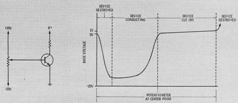
Fig. 9 Transistor base-voltage diagram.
Summary
Some of the more important characteristics of transistors have been discussed in this article, and the effects of changes in the associated components have been examined.
Because of the myriad of transistors available and the vast number of circuits in which they can be used, it is impossible to anticipate all the reactions to circuit defects.
Probably the most important thing to remember when trouble- shooting transistor circuits is that the average DC voltage between the base and emitter of a conducting transistor always will remain essentially constant, although in pulse applications a meter will indicate otherwise. Nonetheless, if a scope is used, it will be found that during conduction time, the average DC voltage remains nearly the same.
If a silicon transistor is considered, the emitter-base voltage is about .7 volt, and it will remain so as base current is increased from cutoff, through the normal operating range, and into saturation. This may be visualized by examining the circuit and curve of Fig. 9.
This circuit, which we have dubbed the "Anderson Handy Dandy Transistor Eater," is constructed so that the voltage to the base of the transistor may be varied from -20 volts to +20 volts. With the potentiometer set to the center of its range, the base voltage is zero and the device is cut off by lack of bias. As the voltage is increased in a positive direction, conduction be gins when the voltage, reaches barrier, or turn-on, potential for the transistor (0.7 volt for silicon and .3 volt for germanium). Further turning of the potentiometer increases the voltage very slightly, although the base current does increase, until the maximum base-current rating of the device is exceeded. At this point, the transistor is "eaten", or destroyed, by the circuit.
If the potentiometer is turned in the opposite direction from mid range (toward negative), the base voltage decreases to the point of reverse base current. Turning the shaft slightly further will not increase the voltage, although the current increases. This is similar to the normal action of a zener diode.
Then, as the shaft is rotated further, the maximum reverse-current rating of the device is exceeded, at which point the circuit again "eats", or destroys, the transistor.
This circuit requires very little skill to build; in fact, it can be "built" entirely by accident. The skill is required to prevent "building" it while troubleshooting a transistorized circuit, and also to recognize that it has been "built" when some part has failed in a solid-state circuit.