Most transistor failures are of the catastrophic type, such as open or short circuits, and can be found without guesswork by use of the simple tests described in the following paragraphs, each of which has been tried and proven in ELECTRONIC SERVICING'S lab.
Use Your Scope to Check Transistors
One method of using an oscilloscope as a read-out device to test transistors is shown in Fig. 1. All base-emitter or base-collector junctions of a transistor exhibit diode characteristics. That is, when the element made of "P" material is positive relative to the other element made of "N" material, electrical resistance of the junction is at minimum. Conversely, negative voltage applied to the "P" element and positive voltage applied to the "N" element will cause a near-open circuit between the two elements.
These junctions also will rectify.
The emitter-collector path involves a series connection of two dissimilar and opposite-polarity "diodes"; because of this, emitter-to-collector rectification is very inefficient, and related test results indefinite.
Interpretation of the scope wave form is the only difficult part of this test; photographs of typical wave forms are shown here to guide you.
Signals supplied to both the vertical and horizontal amplifiers in the scope are changed by the condition of the transistor junction.
A horizontal line, as shown in Fig. 2A, indicates an open circuit; a vertical line (Fig. 2B) indicates a short across the test leads. (In fact, the scope is pre-set by shorting and opening the transistor test leads be fore the test is started. The "H" in put on the scope in Fig. 1 is the external horizontal sweep input, and the sweep selector must be set to the "EXT" position. With nothing connected across the test leads, adjust the horizontal gain control for a horizontal line of about one-half the width of the scope screen. Short the test leads together and adjust the vertical gain control and range switch for a vertical line of about the same height as the length of the horizontal line in the previous step.
Focus and beam intensity of the scope should be adjusted normally.) Typical waveforms for a good germanium transistor tested out of circuit are shown in Fig. 3. As shown, connection of a specific test lead to a specific transistor element produces a definite and individual pattern; this characteristic enables you to identify the polarity of di odes or transistors. Otherwise, it is not necessary to observe polarity in connecting the test leads; the right-angle waveform will face the opposite direction if the leads are reversed or if a transistor having opposite polarity is tested.
In the base-emitter and base-collector tests, silicon transistors produce the same waveforms as germanium types (except for the Zener effect shown in Fig. 4A, which has been evident in all the base-emitter tests of silicon’s I have made so far), but emitter-collector tests of silicon’s (Fig. 4B) indicate an open circuit.
Sharp corners on the scope wave forms are the hallmark of a good diode or a good transistor junction. This also is true during in-circuit tests. If there is a doubt, remove the transistor for a more definite test.
----------------
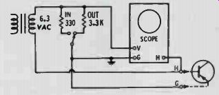
Fig. 1 Schematic of a transistor testing adapter for use with almost any oscilloscope.
Both vertical and horizontal deflection voltages are supplied by the adapter, and no locking of the scope is needed. Two values of resistors are shown: 330 ohms for in circuit, and 3.3K ohms for out-of-circuit transistor or diode tests.
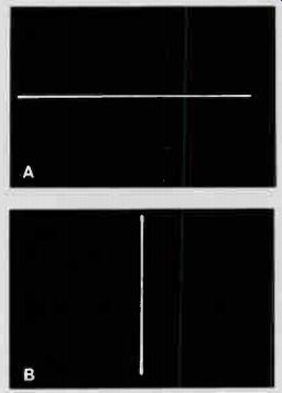
Fig. 2 Single straight lines produced by open or shorted transistors (following
the simple pre-adjusting explained in the text). (A) A horizontal line indicates
an open across the test leads. (B) A vertical line indicates a short across
the test leads.
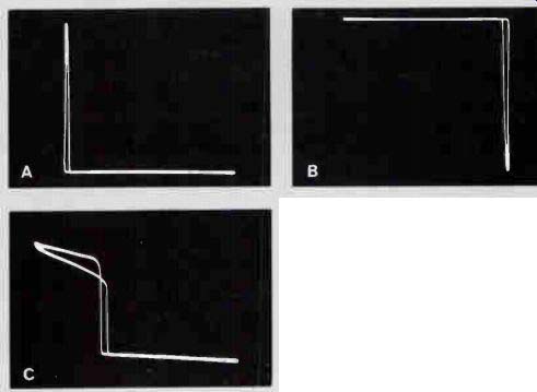
Fig. 3 Waveforms typical of most normal germanium transistors. (A) PNP polarity
transistor with base connected to "H" and emitter
(or collector) to "G". A diode with the cathode connected to "H" and
the anode to "G" will produce the same waveform. (B) The same PNP
transistor with the base connected to "G" and the
emitter (or collector) connected to "H". A diode with cathode connected
to "G" and anode to "H" produces the same waveform. (C)
A PNP transistor with the emitter connected to "H" and the collector
to "G". Rectification is inefficient, and scope gain must be increased
to obtain a large waveform.
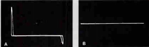
Fig. 4 Silicon transistors present further problems.
(A) One type of NPN-polarity silicon transistor with the base connected to "G" and emitter to "H". The negative-going tip on the right is caused by Zener effect (actually, zener diodes produce a longer tip)-it is not scope overload, nor does it appear in the base-collector waveform. (B) Collector-emitter tests indicate an open circuit when the transistor is a silicon type.
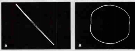
Fig. 5 Waveforms produced by resistance, capacitance or inductance atone,
without a transistor. (A) A 3.3K-ohm resistor across the test leads produces
this tilted waveform. (B) A 0.47-mfd capacitor or a filter choke across the
test leads produces a near-circle.
-------------
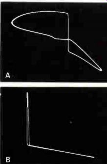
Fig. 7 In-circuit waveforms.
(A) Emitter-to-collector waveform produced by a PNP germanium transistor connected to an unloaded audio-output transformer. (B) Emitter-to-base waveform produced by the same transistor, including bias resistors and electrolytic coupling capacitor.
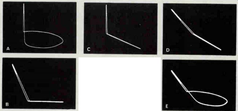
Fig. 6 Waveforms of a transistor with added resistance or capacitance.
(A) A PNP germanium transistor with the emitter connected to "G", the base to "H", and a .25-mfd capacitor in parallel. (B) The same transistor connections with a 3.3K-ohm resistor in series between base and "H". (C) The same transistor connections with a 3.3K-ohm resistor in parallel between base and emitter. (D) A PNP germanium transistor with the emitter connected to "G", the base to "H" through a 6.8K-ohm resistor, and a 6.8K-ohm resistor in parallel with the base and emitter. The waveform approaches that of a pure resistance, but the "diode" corner is still visible. (E) The same transistor in (D) but with emitter connected to "G", the base to "H" through a 6.8K-ohm resistor, and a .068-mfd capacitor in parallel with base and emitter.
-----------------
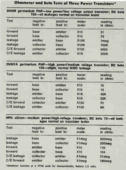
Ohmmeter and Beta Tests of Three Power Transistors 2N408 germanium PNP- low power/low voltage output transistor; DC beta 150-all leakages normal on transistor tester
2N301A germanium PNP- high power/medium voltage transistor; DC beta 130-slight, normal ICED leakage
NPN silicon-medium power/high-voltage transistor; DC beta 70-all leak ages normal on transistor tester
----------
Waveforms produced by resistance, capacitance or inductance alone, without a transistor or diode, are shown in Fig. 5. Comparable waveforms produced by these characteristics and transistor junctions, as might happen in-circuit, are shown in Fig. 6. Two actual in-circuit waveforms are shown in Fig. 7 (the 3.3K-ohm out-of-circuit resistor was used to intensify the obscuring effect of the circuit components). Be certain the power is turned off to any circuits being tested.
Some of the advantages of this method of testing transistors as though they are rectifying diodes are as follows:
• Extreme speed. Just attach the test leads in sequence to the base emitter, base-collector and emitter collector. A short or open "result" indicates a defective transistor.
• No charts or scales. Just select the value of resistor for in-circuit or out-of-circuit tests; that's all.
Disadvantages of this test method are as follows:
Using A Curve-Tracer To Test Transistors
More sophisticated tests of transistors can be made with curve tracers. We presently are conducting evaluation tests on curve tracers manufactured by Eico and Jud Williams, and hope to have our report ready for the December issue of ELECTRONIC SERVICING. Transistor Beta Testers No shop should be without a transistor beta and leakage tester.
In addition to the accuracy of the reading, the equipment makes a favorable impression on your customers who see you use one.
DC beta is the ratio of collector current versus base current. Most commercially built transistor testers vary the base current until a pre determined amount of collector current is read on the meter, then the meter is switched to read the base current. The meter scale is calibrated as DC beta.
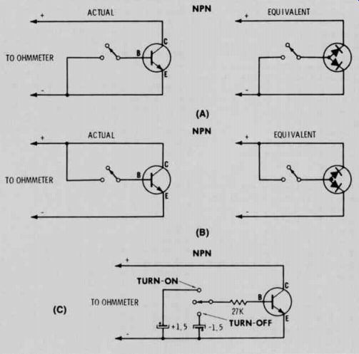
Fig. 8 Simple turn-off and turn-on tests of transistors.
(A) The collector-emitter resistance increases when the base is emitter-a fairly good test. (B) The collector-emitter resistance decreases when the base is collector-a false test of no value. (C) A switch, resistor and two batteries permit accurate turn-off, meter tests-accurate indication of the transistor condition can leads must be changed during the test.
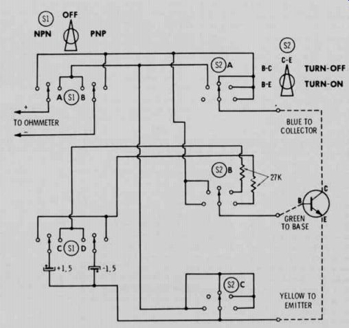
Fig. 9 Complete schematic of an adapter you can build which permits quick
and accurate turn-off, turn-on and ohmmeter tests without moving ohmmeter or
transistor clip leads-a very good method.
To avoid interpreting wrongly the DC beta reading a tester might accurately give us, we should have some understanding about the significance of such tests. Because so many transistor types have been manufactured, a transistor testing manual which would give the control settings of the tester for each transistor, to permit the use of a good-bad scale, is not practical.
Also, the beta reading varies with the collector current used during the test. We, the technicians, must decide the limits that are acceptable in beta readings-often with out sufficient information on which to base this judgment.
A transistor with a DC beta of 150 does not automatically produce twice the AC gain of another transistor of the same type which, when tested, indicates a beta of 75. There are several reasons why this is true.
The same circuits that stabilize against undesired changes caused by heat variations also partially stabilize against variations in average emitter current. Consequently, the more effective the heat stabilization of the circuit, the less AC gain variation will be observed when transistors of different DC beta are used. A transistor with a low DC beta might produce normal gain if the circuit can supply the added base current. However, the input resistance of the transistor will be lower, and this could have a noticeable effect on AC gain because of the change in impedance matching.
Ohmmeter Tests
Ohmmeter tests of germanium type transistors and diodes are quite informative, but such tests are of questionable value for checking silicon devices, for which most ohm meter readings normally indicate a nearly open circuit.
The accompanying table compares the ohmmeter readings of individual transistors and not those representing average conditions. Notice that only the forward bias readings of base-emitter and base-collector of the silicon transistor are low enough to have any significance in an ohmmeter test. Some of these ohmmeter readings will change from the heat of a persons fingers.
Also, the table does not show the completely different readings obtained if another ohmmeter scale is used, or if a meter with a different value of ohmmeter battery voltage is substituted.
Despite all these limitations, nearly all germanium and many silicon transistor defects can be found with ohmmeter tests; because most failures are absolute, borderline or questionable results are seldom obtained.
Turn-Off and Turn-On Tests
Ohmmeter readings combined with simple turn-off and turn-on tests provide an easy method of determining the ability of the base to control collector-emitter current, plus adequate leakage checks.
The collector-emitter resistance (in the forward-bias polarity) increases when the base is connected to the emitter, as shown in Fig. 8A. This is true, but not complete, transistor action, because a small amount of voltage is developed between base and emitter when the base is floating, and this voltage acts as forward bias on the base, which reduces the collector-emitter resistance. Connecting the base to the emitter is the simplest type of turn-off test.
Logic indicates that the circuit of Fig. 8B should be a simple, but good, turn-on test. A low reading on the ohmmeter is produced when the base is connected to the collector. But examining the diode equivalent schematic reveals that the positive ohmmeter lead now is connected to the base, which is for ward biased relative to the emitter and, consequently, will be indicated as a low resistance. This is a false turn-on test, and is of no value.
True transistor action can be tested by the circuit shown in Fig. 8C, which keeps the collector isolated from the base as the base is supplied with forward bias, no external bias or reverse bias. Experience has proven the test results to be very good, but the operational drawback of changing leads increases the possibility of poor connections, not to mention loss of time.
A complete adapter that provides all connections for ohmmeter turn off and turn-on tests is shown in Fig. 9. Neither the transistor nor the ohmmeter leads require reversing or changing, and a transistor can be identified as a PNP or a NPN by the readings obtained when those two positions of S1 are tried.
The same 2N408 used to obtain the readings in the accompanying table measured 200 ohms on the turn-on position of S2, 6K-ohms on the C-E position, and about 100 megohms on the turn-off position.
No hair-splitting decisions are necessary to conclude that this transistor is normal.