The function of a preamplifier is to allow the user to select a signal from one or other of a variety of sources--such as a radio, a tape recorder, a gramophone pick-up or a CD player--to offer an input impedance and signal level handling capacity which is appropriate to the chosen source, to adjust the amplitude/frequency characteristics of the input signal, if necessary, to give the required tonal quality, to amplify the signal, if required, to the 0.5-5V rms level needed to drive an audio power amplifier, and, finally, to provide this output signal at an adequately low impedance level.
In earlier, thermionic tube operated audio systems the minimal functions of a preamplifier were often performed by a simple selector switch and volume control at the front end of the power amplifier, or perhaps by an additional tube, with facilities to switch between one or two alternative frequency response shaping networks. These would be used to provide selective attenuation or gain adjustments, either by passive RC networks or by negative feedback arrangements.
It was unusual at this period to employ a separate preamplifier unit, so where more extensive signal manipulation circuitry was provided- as in the case of the Williamson, or the Brimar preamplifier shown in FIG. 16 - it was usually incorporated within the main amplifier housing, an arrangement which is now described as an integrated amplifier. It was not until the advent of the transistor, with its small size, its low power requirements, its absence of AC operated heater circuitry and its low heat generation, that the advantages of segregating the low signal level input circuitry and the high signal level power stages and power supply wiring could be seen as a normal feature in high quality systems.
It is also required that the signal manipulation and amplification carried out by the preamplifier shall be done without significantly impairing the distortion or the signal/noise ratio of the input signal, though the weight attached to the term significantly will probably be a matter for debate between the designer and his critics-- who may be insulated by their armchairs from the need, in practice, to make accommodations between desirable, but not always mutually compatible, requirements.
A friend of mine, for whom the purchase, use, and subsequent resale of Hi-Fi exotica appeared to be a major hobby interest, told me that in his experience there were greater differences in the sound of different preamplifiers than there were between comparably well-designed power amplifiers. If he was correct in this belief, it is probable that the tonal differences he had noted had their origins in the various parts of the circuit in which the gain/frequency response of the system had been deliberately modified, for example to compensate for the skewed amplitude/frequency response used in the recording of an LP or EP gramophone disc.
Gramophone Record Replay Equalization Characteristics
Various combinations of recording pre-emphasis and replay de-emphasis have been proposed for use in gramophone record reproduction. Of these, the most relevant is the method recommended in the RIAA:BS1928/1965 specification, in that this has been adopted, on a world-wide basis, for the manufacture of 33 and 45rpm vinyl discs.
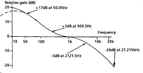
The proposed pre-emphasis characteristics were based on a recognition of the practical problems in disc manufacture and reproduction using velocity sensitive (e.g. electromagnetic) cutting and replay heads. These realities also influence the extent to which electrical headroom is needed- a matter which I will explore later on. In its original form, the RIAA specification required a replay characteristic of the form shown in FIG. 1, in which the shape of the replay response was defined by three time constants, 3180~ts, 318~ts and 75~ts. There has, however, been a recent amendment to this specification, in acknowledgement of the inevitable VLF noise present on LP disc replay, to include an additional LF roll-off defined by a 7950~ts time constant, as shown in the dashed line curve in FIG. 1.
The need for the rising replay gain characteristic below 1kHz is because of the typical maximum allowable LP/EP groove separation of 0.01 cm, which limits the magnitude of the permissible recording cutter excursion (to avoid adjacent groove breakthrough) with a consequent linear reduction in replay stylus velocity (and output voltage from the pick-up) with decreasing frequency. The concept of HF recording pre-emphasis, followed by replay de-emphasis, was initially adopted for 78rpm records, so that the reduced level of treble, on replay, would lessen the irritating audible hiss due to the emery powder loading of the shellac discs. This arrangement has been retained even in the case of the much quieter vinyl surfaces. The most commonly used of the several 78rpm equalization specifications was similar to the RIAA but with time constants of 3180μs and 450μs to 1kHz, and then with a fall off in gain defined by a 50μs time constant to 21 kHz.
Replay Equalization Circuitry
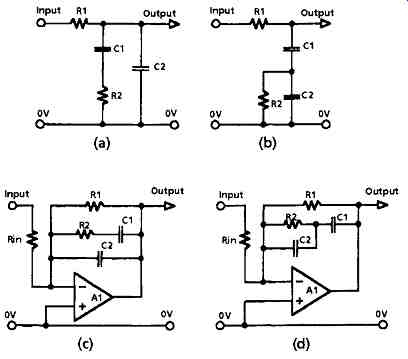
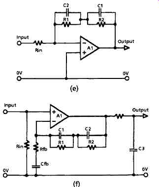
There are a number of circuit arrangements which will generate the required RIAA replay response curve for use with velocity sensitive gramophone pick-up transducers, and I have shown the more commonly used circuits in FIG. 2. Of these, the simplest, and therefore, in the opinion of the purists, the most desirable options are the two passive networks shown in FIGs 2a and 2b. However, in order for these to function correctly they must introduce an attenuation of 20dB at 1kHz, and this will require some additional amplification to restore the original signal level. Also, for the frequency response of the networks to conform accurately to the RIAA curve, it is necessary for them to be driven from a very low impedance source and for the output load to offer an impedance which is high in relation to R1. In practice, these requirements imply the need for further amplification or buffer stages preceding or following the passive network, so the presumed advantages of simplicity and absence of (possible distortion introducing) active components are lost.
The layouts of FIGs 2c, 2d and 2e can be arranged so that they can be fed directly from the pick-up cartridge, with Rin chosen to provide the manufacturers specified loading for the cartridge. This layout also offers a low output impedance to any following stages which avoids the need for additional pre- and post-amplification.
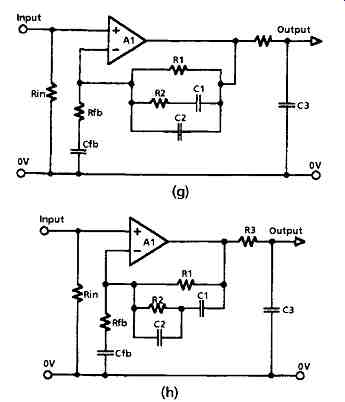
All three of these circuits use shunt feedback, which has the relative disadvantage that the input thermal noise is determined by the source impedance in series with Rin , which will be worse, at low to mid-frequencies with an inductive transducer, than that given by a equivalent series feedback layout. A simple calculation would suggest that the source noise level for a series feedback circuit, such as that of FIG. 2g, when used with a pick-up cartridge having a DC winding resistance of 2200 ohms (connected in parallel with a 47,000 ohms load resistor) will be 0.83gV. (This figure is the room temperature value seen at the input of a feedback circuit of the kind shown in FIG. 2g, with a 20Hz-20kHz measurement bandwidth.) The calculated value for a shunt feedback system, of the kind shown in FIG. 2e, with an input (pick- up load) resistor of 47,000 ohms, will have a noise voltage of 4.24uV under the same measurement conditions.
However, these figures are modified by the fact that the measurement bandwidth for an RIAA equalized gain stage is not 20kHz, but less than a tenth of that figure, which changes the noise output figures to 0.24gV and 1.22gV respectively. Also, pick-up cartridges will have a significant value of inductance - the quoted value for a Shure M75 cartridge being 450mH -- and this will increase the source noise voltage at the upper end of the audio pass-band. The effect of this is to alter the relative character of the noise given by these two systems, so that the noise from a series-type circuit is a high pitched hiss, while that from a shunt-type circuit is more of a low pitched rustle.
There are also a few other advantages offered by shunt feedback RIAA circuits such as those shown in FIGs 2c, 2d and 2e. Of these, the most important, in practice, is that they are largely immune to very short duration input overload effects, which can be caused by voltage spikes in the cartridge output arising from dust and scratches on the surface of the record. These short duration overloads can greatly exaggerate the clicks and plops which are such a nuisance on vinyl disc replay. Also, they have, in theory, a lower level of distortion (see Taylor, E.F., Wireless World, April 1973, p. 194) -- although this is a matter only of academic interest in the presence of the 0.5-1% THD generated at 1kHz by a typical pick-up cartridge ( Hi-Fi News and Record Review, October 1982, pp. 59-68). Shunt feedback layouts can also give a precise match to the RIAA specification, which a series feedback circuit, as it stands, will not. This is because any series feedback layout having a feedback limb which decreases in impedance with frequency will tend to unity gain at high frequencies, whereas the RIAA specification stipulates a gain curve which tends to zero. Unfortunately, in many preamplifiers of commercial origin, which use series feedback RIAA stages in order to obtain the lowest practical (input short-circuited) noise levels, this error is ignored, even though its effect can easily be seen on an oscilloscope ( Wireless World, October 1982, pp. 32-36) and the tonal difference which it introduces can equally easily be heard by the listener.
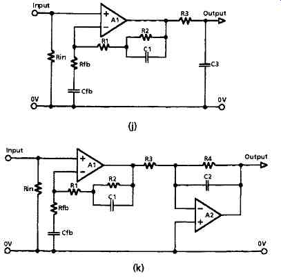
This error has been corrected, in the case of the circuit layouts shown in FIGs 2f, 2g and 2h, by adding a final RC lag network, R3/C3, in which the required component values will depend on the gain of A 1 at 20kHz. The gain reduction in the 1kHz-21kHz part of the pass-band required by the RIAA spec. can be made more simply by dividing the circuitry used to provide this response into two parts- as in FIG. 2j - where R1, R2 and C1 generate the frequency response curve from 30Hz to 1kHz and R3 and C3 provide the 75us time constant needed for the 1kHz-21kHz part of the spectrum. A possible drawback with this circuit (which will also apply to any final frequency response correction lag network), depending on the nature of the following circuitry, is that the time constant of R3/C3 will be affected by the circuit load impedance, which is, for the purposes of this calculation, in parallel with R3. This difficulty is removed by the use of an active output integrator, shown as A2 in FIG. 2k, where R4/C2 provide a 75us time constant. The only likely problem with this arrangement is that the circuit introduces a phase reversal, which may not be desired.
The required component values for these networks were originally calculated by Livy and quoted in an article describing a simple RIAA equalizing stage (Livy, W.H., Wireless World, January 1957, p. 29) shown in FIG. 3a. The calculations were recast by Baxandall in a slightly more accessible form, and quoted in a reference work (Baxandall, P.J., Radio, TV and Audio Reference Book, S.W. Amos, ed., Newnes- Butterworth, Section 14), in the course of an excellent review of RIAA equalization options.
Using the formulae quoted by Baxandall, the required values for R1, R2, C1 and C2 in FIGs 2a, 2c and 2g can be determined by:
R1/R2 =6.818 C1 R1 = 2187us C2 R2 = 109us
For FIGs 2b, 2d and 2h the component values can be obtained from:
R1/R2 = 12.38 C1 R1 = 2937us C2 R2 = 81.1us
Similarly, in FIGs 2e and 2f, the values are given by:
R1/R2 = 12.3 C1 R1 = 2950us C2 R2 = 78us
Practical Circuit Layouts
In tube amplifiers the most common RIAA equalization circuitry was of the kind shown in FIG. 3a, due to Livy, in which the frequency dependent feedback network is connected between anode and grid of a high gain amplifying tube- typically a pentode of the EF86 type. Translating this type of circuitry into a transistor form using a single bipolar junction transistor (see Tobey, R., and Dinsdale, J., Wireless World, December 1961, pp. 621-625, and also Carter, E., and Tharma, P., Wireless World, August 1963, pp. 376-379), encountered the two problems that the input impedances were much lower than was the case with a tube amplifier and that the available gain was inadequate to achieve the required frequency response from the stage, especially at the low frequency end of the RIAA curve where a gain of +20dB with respect to that at l kHz was needed. The normal approach to this problem was to increase the value of R1, which increased the LF gain at the expense of accuracy in conforming to the lower end of the RIAA curve.
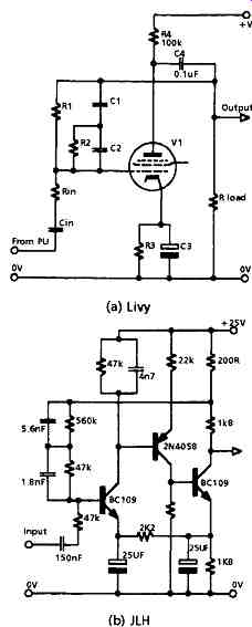
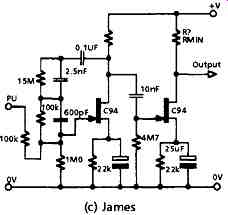
FIG. 3
In a rather later circuit of my own ( Wireless World, July 1969, pp. 306-310), shown in FIG. 3b, I elaborated the single transistor circuit into a triplet, which greatly increased the available gain and also allowed a third order (18dB/octave), 30Hz high pass rumble filter to be implemented using the negative feedback path between the two BC 109 emitters.
The availability of junction FETs, which approached much more closely in their operating characteristics to the thermionic tube- with the exception of a much lower gain - encouraged their use in circuits based on their tube precursors, and an FET based design due to James, using some early devices of this type (James, D.B.G., Wireless World, April 1968, p. 72), is shown in FIG. 3c.
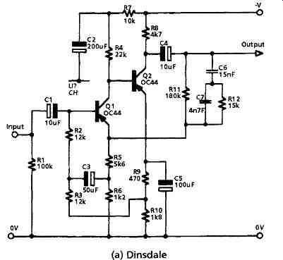
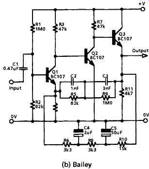
The circuit due to Dinsdale (Dinsdale, J., Wireless World, January 1965, pp. 2-9), shown in FIG. 4a, was one of the earliest of the transistor based RIAA equalization circuits to use series feedback around a gain block having a useful amount of stage gain, and became the standard design adopted by a large number of Hi-Fi manufacturers, though with silicon planar transistors rather than the germanium diffused junction types used by Dinsdale. A problem with this design was that the equalizing network applied a capacitative load on the output of Q2, which reduced the gain of Q2 at the upper end of the audio spectrum, although, in practice, this might go some way to remedying the inadequate HF attenuation which is characteristic of the series feedback RIAA system. This problem of falling HF gain was remedied by Bailey (Bailey, A.R., Wireless World, December 1966, pp. 598-602) by the use of a transistor based version of the tube Ring of Three shown in FIG. 4b. This had a low impedance, emitter-follower output stage, and also incorporated a second-order high pass rumble filter, via R6-R10, to attenuate signals below 30Hz.
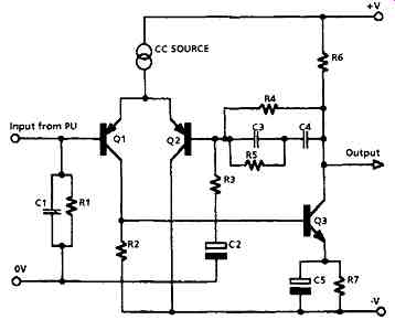
FIG. 5 Direct coupled RIAA stage
With the growing use of symmetrical +/- power supply lines, the discrete component version of the RIAA stage shown in FIG. 5 has become popular, either in the form shown, or in its complementary version, and usually with some elaboration of the general structure. For a simple design with normal bipolar junction transistor inputs, PNP input devices will normally be chosen because of their better noise performance, although this design decision will be influenced by the availability of application specific components such as the NPN super match pairs described below. This circuit arrangement illustrates one aspect of modem design practice, which favors DC coupling to minimize the use of capacitors in the signal path (except when their use is forced, as, for example, in the RIAA frequency correction network). If Q1 and Q2 were a matched pair it would be possible also to dispense with the DC blocking capacitor (C2) in the feedback line. The capacitor, C1, across the pick-up load resistor will have a value recommended by the cartridge manufacturers to obtain the flattest possible frequency response.
Most contemporary RIAA equalizing circuits are based on versions of FIGs 2g or 2h, though there is an increasing trend to the use of versions of FIGs 2c and 2d in which the output from the pick-up cartridge is amplified by a low noise, fiat frequency response gain stage, and then presented to the RIAA stage at a signal and impedance level at which the noise level differences between shunt and series connected NFB networks are insignificant. The differences, at the high quality end of the market, between one manufacturer's products and another, now relate to whether integrated circuit or discrete component gain blocks are used as the amplifying stages, and, if the latter, the type of component layout chosen.
Very Low Noise Input Systems
Towards the end of the vinyl era -- to the great regret of many gramophone record users, the manufacture of the 12 inch LP disc was discontinued in the late 1980s by the major record manufacturers in favor of the more robust and less expensive compact disc--the phono pick-up cartridge design which had come to be preferred by the connoisseurs was one using a moving coil type of construction, rather than the moving magnet or variable reluctance style of mechanism which had dominated the high quality end of the audio market for the previous forty years. The lower mass of the moving coil transducer, and its more effective linkage to the stylus assembly allowed an improvement in the dynamics and stereo channel separation of the system, and the much lower inductance of the pick-up coils greatly improved its high frequency response. However, the typical mean signal level output voltage from such a cartridge might well be only some 50-500uV rather than the 3-5mV output voltage which would be given by a moving magnet transducer, and this required a different approach to RIAA equalized input stage design.
Moving coil pick-up cartridges had been manufactured for many years before there were suitable components for the construction of electronic head amplifiers, and the necessary amplification was provided by an input step-up transformer of the type which had been employed for the same purpose with low output-voltage microphones.
However, the use of an electronic gain block offered advantages in terms of wider bandwidth and greater freedom from unwanted hum pick-up.
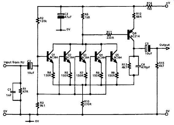
The main approach employed by the audio circuit designers was to place this gain block between the pick-up cartridge output and the input to the RIAA stage. This way was chosen because it was easier at that time to design a flat frequency response head amplifier than to make a switched gain RIAA stage with a noise level which was fifty times lower than the current norm. For such a gain block to have such a low input noise level it would need a lower input circuit impedance than would be found in a normal small-signal transistor amplifier. There are various ways by which this could be achieved. Of these, the most obvious was to connect a number of input devices in parallel, as shown in the circuit of FIG. 6, due to Naim. Here five transistors have been arranged in this way, which would, other things being equal, reduce the input base spreading resistance (that distributed resistance between the base connection on the chip and the active base region of the transistor) to one fifth, and reduce the input noise voltage to 1/~/5 or a little less than a half. Some of this input noise improvement is lost, unfortunately, because of the need to include additional emitter resistors to ensure current sharing between the unmatched input devices.
Naim NAC 20 head amp
Another approach, rather more suited to the DIY constructor than the large-scale manufacturer, is to use a small-power transistor as the input device, because these will have a larger chip size and, in consequence, a lower base spreading resistance.
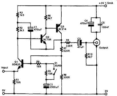
However, the use of such input transistors might require a degree of selection to find those having the best noise level. An example of this type of circuit is shown in FIG. 7, for a 30/60 ~ head amplifier, particularly suited to very low impedance, low output voltage cartridges such as the Ortofon MC20. In this, Q1, a BD435 small- power transistor, is operated as a grounded base amplifier with a load resistor (R3) which is bootstrapped to increase the stage gain, while NFB is applied via R7, R4 and R5. The output impedance at Q1 collector is reduced to a low level, as seen at the output, by Q2 and Q3, which are connected as a high gain, compound emitter-follower. The circuit is designed to be powered from a pair of 1.5V AA cells, from which the current drain is 1.5mA/channel. The -~ 1 dB bandwidth is 10Hz-40kHz, and the THD is less than 0.02% at 1V output at 1kHz.
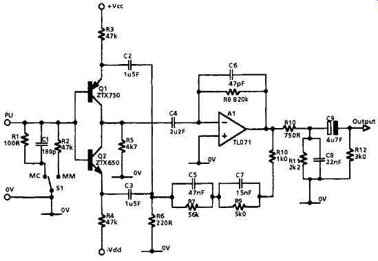
FIG. 8 Quad M~MM input circuit
The other way in which the input resistance of the amplifier may be reduced is by operating the input devices in push-pull, which will double the gain and halve the effective noise resistance. An elegant way of doing this is that used by Quad, and shown in FIG. 8. This takes advantage of the fact that a silicon bipolar junction transistor can operate as an amplifier, though admittedly only at relatively low input signal levels, when its collector voltage is no greater than that on its base. Operation at such a low collector voltage will help to reduce the shot noise component due to collector-base leakage currents in the input devices. Quad used this layout in all their pre-1994 RIAA input stages, with component values being chosen to suit their use either as moving magnet or as moving coil input arrangements. Although the main op amp gain block, A1, is operated in the shunt feedback mode, the circuit as a whole uses series FB because of the interposition of Q1 and Q2. R10, R11 and C8 provide the necessary additional HF attenuation to correct the inevitable series FB gain error.
Low Noise Devices
Bipolar junction transistors
The concept of using multiple, parallel-connected, input transistors as very low noise input devices offered an opportunity to the IC manufacturers to use their existing fabrication techniques to make low noise matched pair transistors where each transistor was, in reality, a large number of parallel-connected devices - distributed across the face of the chip to average out their characteristics. The National Semiconductors LM194/394 devices were early examples of this type of construction, and offered input noise resistance figures of the order of 40 ohms, and bulk (emitter circuit) resistances of about 0.4 ohms. Recently, Precision Monolithics have offered their MAT-01 and MAT-02 super-match pairs, and their SSM-2220 and SSM-2210 equivalents, which are respectively NPN and PNP matched dual transistors, which have input noise resistance values less than 30 ohms. An ultra-low noise gramophone pick-up input head amplifier stage, based on the SSM-22 l0 and SSM-2220 super-match pairs, is shown in FIG. 9.
This circuit makes quite an interesting design study, with the Q2 pair of transistors acting as a cascode load for Q1 to increase the input gain, with the Q3 pair acting as a current mirror to sum the outputs of the two halves. Because the bases of Q2 are held at approximately 3V, the collector voltages for Q1 are clamped at about +2.4V, which offers adequate input headroom while still being low enough to minimize collector- base leakage currents. Constant current sources form tail loads for Q1 and collector loads for Q4. In addition to increasing the stage gain, this assists in rejecting signal breakthrough .from the power supply rails. Switch S1 allows a choice of input resistances and a choice of stage gain levels, 15 or 150", to suit MM and MC pick-up inputs.
Junction FETs
Very low noise JFETs have been available for at least ten years from specialist manufacturers such as Hitachi, Siliconix and Intersil, and, more recently, have also been readily obtainable in dual matched pairs, specifically intended for use in amplifier input stages. The availability of FETs in matched pair forms avoids two of the problems inherent in these devices; that the drain current vs. gate voltage relationship is influenced by so many factors, such as doping level, channel geometry and the distribution of doping impurities, that their drain current cut-off voltage, [Vgs(off) ] and their drain current at zero gate voltage (IDss) are very variable from one device to another, so that a considerable degree of selection would be necessary to obtain a balanced pair.
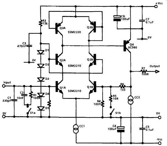
FIG. 9 Super-match pair head amp
In terms of noise levels, JFETs traditionally suffered from a higher level of flicker (I/f) noise than junction transistors. Also their channel resistance is much higher- because of their method of construction- than those of BJTs. Improvements in 1/f noise have been made by greater care in their physical construction and the channel resistance has been lowered by connecting a large number of channels in parallel, in a similar way to that used in making a junction transistor super-match pair.
A very high performance RIAA corrected input stage, due to Spectral Inc., is shown in FIG. 10. This also has a cascode connected input stage but with the bias offset voltages of Q2a and Q2b used to provide the 2-3V drain voltage required by Q1a and Q1b. Q3a/Q3b provide a second gain stage, with Q4a and Q4b forming a current mirror collector load for Q3. A symmetrical emitter-follower pair is used to lower the preamplifier output impedance, to allow it to drive a low resistance RIAA equalizing network in the feedback path to Q1b. As is current Hi-Fi practice in the USA, aimed at lowering LF phase errors, there are no DC blocking capacitors in the signal path, so RV1 is used to trim out any small residual DC output offset.
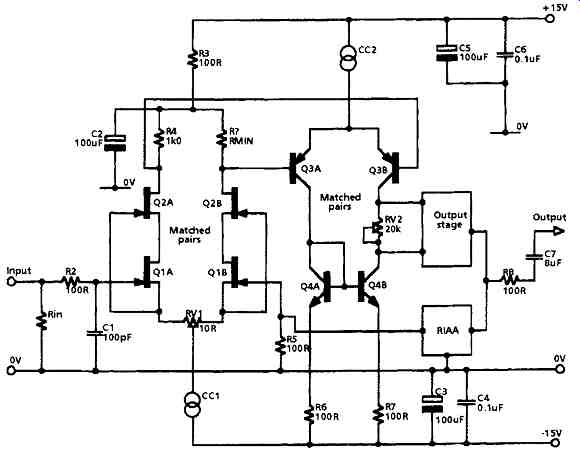
FIG. 10 Spectral RIAA input stage
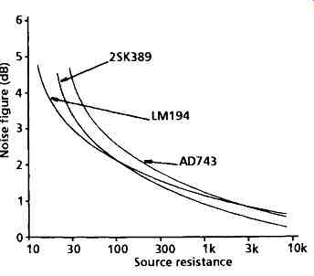
FIG. 11 JFET/BJT noise figures
The input noise resistance of an FET, at drain voltages which are low enough to avoid significant drain-gate leakage currents, is determined principally by the resistance of the channel, and this is related to the slope (gfs) of the drain current/gate voltage curve, in an ideal device, by the equation:
R(n) = 0.67/gfs (ohms)
As an indication of the relative performance of contemporary JFET and bipolar transistors, the noise characteristics of LM194 and 2SK389 monolithic matched pairs are shown in FIG. 11. This shows that, for input circuit resistances of above 100 ohms, the 2SK389 FET has a lower noise figure than the best of the bipolar devices.
Low noise op amps Inevitably, all improvements in device manufacture, as applied to discrete components, will find their way into the field of IC manufacture, and this results, in the present case, in the availability of audio type ICs, such as the Analog Devices AD743 bifet op amp, which has a 10kHz noise voltage of 2.8nV/~/Hz and an output distortion figure of 0.0003% at 1kHz and 5V rms. I have also plotted the noise figure of the AD743 on FIG. 11, on which it appears little worse than that of the 2SK389. Under the circumstances, there seems to be little point in using elaborate discrete component circuits such as those shown in FIGs 9 and 10, as an alternative to an IC, except to provide greater headroom than that would be available from an IC op amp operating from 15V supply rails.
Headroom
Very few topics can have generated as much debate in the audio field as the extent to which the designer should allow for possible input overload in any given circuit, a factor generally referred to as headroom. Sadly, much of this debate has been entirely misguided. The reason for this is that all the sources which provide signals to the preamplifier do have specific output voltage limits. For example, in the case of a tape recorder, either reel-to-reel or cassette type, the recording level is generally chosen so that the peak output signal is not more than 3dB (~/2") greater than the normal span of the recording range. At +6dB, the output THD would probably have increased, in the case of a cassette recorder, from about 0.5% to some 3-5%, and at +12dB (4 ") magnetic saturation of the tape would probably have clipped the peaks of the signal anyway, preventing any further output voltage increase.
In an FM tuner, constraints on the permissible frequency excursions of the broadcast signal impose stringent limits on the magnitude of the modulation, and this is rigidly peak limited before being broadcast- again giving a +6dB maximum likely signal over-voltage limit. In the case of CD the recording engineer will want to use the bulk of the available 16-bit (65,536) output levels, while there is an absolute prohibition on any attempt to go beyond this, so, once again, there is an output voltage ceiling, which is unlikely to be greater than +6dB above the intended maximum recorded level.
This leaves only the vinyl gramophone disc as a source of possibly unlimited peak output voltages, but, here again, at least for recorded signals, there are output level constraints, as shown in FIG. 12. The recording characteristics of the vinyl disc were analyzed by Walton (Walton, J., Wireless World, December, 1967, pp. 581-588), to whom I am indebted for the data on which FIG. 12 is based. Below about l kHz, the electrical output from the pick-up cartridge is limited by the allowable 0.01 cm spacing between the grooves, and the resulting 0.005cm maximum permitted cutter excursion. Above a turnover frequency of around 1kHz the possible closeness of succeeding groove excursions, which control the output voltage, is determined by the shape of the rear face of the cutting head and the linear velocity of the stylus in the groove (which will depend on the track diameter). Beyond about 3kHz there is a limit imposed by the maximum groove accelerations which the cutter head can generate or the pick-up stylus can follow. These are also limited by the groove velocity, and thus depend on the track diameter.
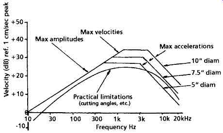
FIG. 12 Maximum recorded levels.
Walton considered that, under optimum conditions, and at a 7.5" groove diameter, a groove modulation velocity equivalent to +30dB at 2kHz, with respect to 1 cm/s, was the maximum which would be cut. The Shure Corporation, which made a specialty of the manufacture of pick-up cartridges with very high record groove tracking ability, claimed that its best models were capable of following a groove modulation of +40dB ref. 1 cm/s at 2kHz, decreasing with increasing frequency. They obviously considered that the musical bells track on their stereo test record, which was cut at a recording level of +25dB at 10kHz, would present a formidable challenge to their competitors- a consideration which lends support to Walton's curve of practical output limits in FIG. 12.
From this analysis, if a recorded velocity of 5cm/s is taken as the normal maximum mid-band signal, the limitations of the recording process will ensure that the maximum modulation velocity which the pick-up will encounter on a very heavily modulated part of the recording will not exceed some 30cm/s. This practical limitation on the pick-up cartridge output voltage was also shown by Wolfenden (Wolfenden, B.S., Wireless World, December 1976, p. 54) using data from Shure, and by Kelly (Kelly, S., Wireless World, December 1969, pp. 548-555) who had confirmed, by experiment, the magnitude of any feasible overload margin.
However, with the same kind of logic which persuades ordinary, sensible motorists that a car which is capable of 150mph is a much better proposition- in a country where the speed limit is 70mph- than one which will only do 90mph, many circuit designers consider it necessary to provide RIAA stage voltage overload margins of 20-30", or greater. Unfortunately, by praising such achievements, reviewers perpetuate the belief that this style of design is both good and necessary. Clearly, some type of gain switching is necessary if the preamp is to cope with the voltage output levels from both MM and MC type pick-up cartridges, but these cartridges will require switch selection of their load resistance anyway, between, say, 47k and 100R, so the provision of a switchable choice between low impedance/high gain, and high impedance/low gain options has become normal practice. In reality, the highest output voltage peaks are likely to be those associated with dust particles, scratches and other blemishes on the surface of the disc, and while it is obviously desirable that such sudden input voltage excursions do not lead to a prolonged paralysis of the amplifier, clipping which is very brief in duration may be acceptable to the listener.
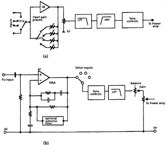
A typical op. amp gain stage, fed from a +15V supply, is capable of a 9.5V rms undistorted output voltage swing. It should therefore be capable of handling, without clipping, the signal from any disc replay amplifier whose normal maximum output level is less than 1.5V rms. For the greatest freedom from signal overload, the gain control should be placed as far forward in the signal chain as possible, as shown in schematic form in FIG. 13a. Unfortunately, with this layout the total noise contributions from the following stages will be present all the time, regardless of gain control settings. The alternative option, shown in FIG. 13b, is to place the RIAA equalization stage between the pick-up input and the input selector switching. Any tone controls or filters, if used, can then be based on unity gain blocks, which if they use the same type of gain stage (such as a low noise op amp) as that used in the RIAA module itself, will not overload if the RIAA module does not. With this type of layout, the preamplifier noise contribution will decrease to zero as the signal level is reduced.
Tone Controls and Filters
In the earlier days of audio, it was taken for granted that there would be shortcomings both in the tonal quality and in the signal to noise ratio of all of the input signals. There would also be deficiencies in the frequency response characteristics of both the input transducers and the loudspeakers, and it was expected that any high quality preamplifier unit would offer comprehensive facilities to allow correction of the electrical output signal. However, there has been a continuous improvement in the quality of the input signal, whether obtained from compact disc, LP record, FM tuner or cassette tape. Similarly, there has been a continuing improvement in LS performance, so that, for example, the bass output is only limited by the physical dimensions of the LS cabinet, or of the listening room, and additional bass boost would be pointless. Faced with this situation, many amplifier manufacturers no longer offer anything other than fiat frequency response amplifier units.
While the flat frequency response approach is probably adequate for most purposes, I feel that there are still a few remaining situations where, for example, high pass rumble filters are useful- such as when a new CD has been mastered from an archive source, and contains significant amounts of LF noise from mechanical sources, or where a blameless recording suffers from low frequency traffic noise intrusions into the notionally silent recording studio - or where the tonal balance chosen by the recording engineer differs from that preferred by the listener. In this case some form of frequency response tilt control would probably be useful. I have therefore shown two design examples of these. The first of these, due to Quad, is shown in FIG. 14, and the second, due to Bingham (Bingham, J., Hi-Fi News and Record Review, December 1982, pp. 64-65) is shown in FIG. 15. I have also shown the layouts for four steep cut filter circuits in FIG. 16.
The filter circuits shown in FIGs 16a and 16b use my own bootstrap design ( Electronic Engineering, July 1976, pp. 55-58) and give a -18dB/octave frequency response. That of FIG. 16a is a 50Hz high pass layout, and that of 16b is a 10kHz low pass circuit. The filter circuits shown in FIGs 16c and 10.16d have the same cut-off frequencies, but use the Sallen and Key layout (Sallen, R.P., and Key, E.L., IRE Trans. Circuit Theory, March 1955, pp. 40--42) which gives a-12dB/octave response. For both filters the turnover frequency is given by the formula:
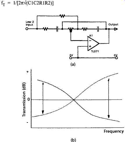 FIG. 14 The 'Quad' slope control
The turnover frequencies can be changed, up or down, by proportional alterations to the resistor or capacitor values. For example, if the values of C1, C2 and C3, in FIG. 16a, are increased by the factor 5/3, the turnover frequency of this filter will be reduced to 30Hz. Similarly, if the values of the resistors, R1, R2 and R3, are halved, the turnover frequency of FIG. 16b will be increased to 20kHz, and so on.
Since the bulk of modem signal sources are not much in need of remedial treatment, I have not included technical descriptions of the wide variety of tone control arrangements which have been evolved over the years. For those seeking further information on these, I would recommend my book Audio Electronics, (Butterworth- Heinemann, 1965, Section 4, pp. 169-189), or an earlier article of mine in Electronics World + Wireless World (July 1990, pp. 636--639).
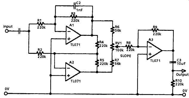
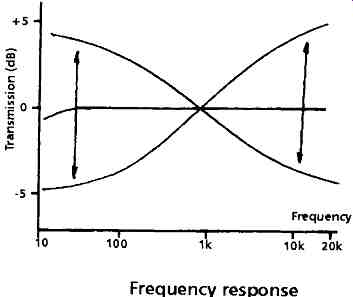
FIG. 15 Bingham's tilt control
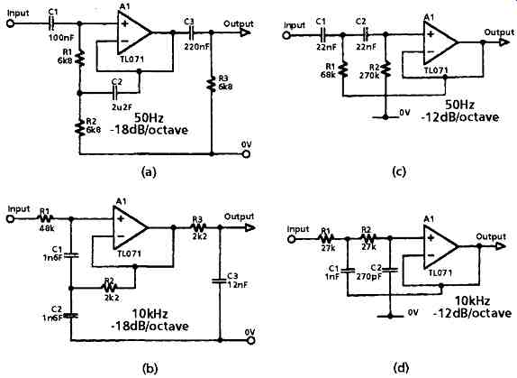
FIG. 16 Steep cut filter circuits
Signal Channel Switching and Remote Controls
The choice between input channels can be made by purely mechanical means, such as a simple rotary switch or a suitable push-button sliding contact arrangement. The only normal difficulty with this system is that the knob or the push-buttons which control the channel selection will be on the front of the preamp box, while the signal inputs between which the electrical choice is to be made all go to sockets on the back face of the box, so that the internal connecting wires which join the one to the other must pass over other parts of the signal circuitry, and may need to be well screened. If the switching element is a relay (preferably sealed, and inert gas filled), or a suitable semiconductor switch, of the kind I have shown in FIG. 17, the input switches can be located close to the input sockets. It will also allow channel selection to be made by an external voltage, and this will allow the convenience of remote control, perhaps by the use of an infra-red transmitter/receiver assembly of the type widely used for similar purposes with TV sets.
Most of the plain on/off types of signal switching, based on discrete components or CMOS analogue switches, of the type I have shown in FIG. 17 offer acceptably low distortion characteristics up to, say, a 1V rms signal level. In the case of the series connected FET switch, shown in FIG. 17c, the value of Rin should be high in relation to the 'on' resistance of the FET to swamp any signal induced changes in the channel resistance. In the case of the CMOS analogue switches shown in schematic form in FIG. 17d, these devices normally are designed to operate with logic level input control voltages, and do not significantly distort input signals so long as their peak-to-peak values lie comfortably between the limits set by the DC supply rails. The extent of the distortion introduced by these devices depends on the output load (which should, ideally, be very high) and on the quality (and cost) of the component itself.
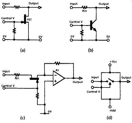
FIG. 17 Voltage controlled switches
Voltage Controlled Gain Systems
While there are a number of low distortion switching circuits available, the techniques proposed for a continuous, voltage controlled, alteration of the amplifier gain are usually much less satisfactory. For simple, low cost signal-level control the FET arrangement of FIG. 18a, in which the FET and the input resistance, R1, form a simple resistive attenuator, is fairly widely used. As it stands, this would have a THD figure, at 1V rms and 1kHz output, of some 10-15%. In the Siliconix file note, AN73-1, it is proposed that negative feedback should be derived from the drain circuit, by way of R2 and R3 (Siliconix suggest that the THD is lowest when R2 = R3 10(R1//Rds//RL) ). This will reduce the THD to about 1-1.5% and although this figure decreases as the signal level is reduced, it is still very much higher than would be acceptable in any Hi-Fi context.
A commercially available alternative to the discrete component (e.g. FET) voltage controlled attenuator is marketed as the Motorola MC3340P IC, a device which was widely used in TV remote control systems. This uses two long-tailed pair circuits in which the gain is controlled by the tail current. By connecting the non-inverting and inverting outputs in antiphase the second harmonic distortion is partially cancelled.
The claimed performance offers a 90dB possible attenuation ratio, a bandwidth of 1MHz, and a THD of 0.2%, worsening to 3% as the attenuation is increased.
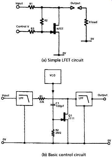
FIG. 18 Attenuator circuits (a) Simple LFET circuit (b) Basic control circuit.
I described the various other available techniques in an earlier article ( Electronics World + Wireless World, April 1995, pp. 320-321), and suggested the use of a very low distortion discrete component design (intended for use in a dynamic range control circuit ( Electronics World and Wireless World, November 1995, pp. 938-940). This gain control circuit was based on a switch-mode attenuator, shown in schematic form in FIG. 18b. In this circuit a high frequency (180kHz) rectangular voltage waveform is used to control the proportion of the time in which the channel is open. This, in turn, is controlled by the 'on to off' ratio of the switching waveform, which can be changed, within the range 5% : 95% to 95% : 5% by a DC input voltage to the waveform generator circuit. This gives an attenuation ratio of about 30dB, and a THD- at 1V rms and 10Hz-10kHz- of less than 0.005%, mainly due to the steep-cut low pass filters used to remove signal components within 20kHz of the switching frequency.
In their application note AN-105, PMI propose an improved version of the system used by Motorola, of which I have shown the circuit in FIG. 19. The THD introduced by this circuit depends on the cancellation of the distortion, mainly second harmonic, introduced by the controlled transistors, Q l-Q4. For this to be adequate, there must be an exceedingly close match between all four transistors, and PMI show this as an application for their MAT-04 monolithic transistor array. PMI claim a THD value of <0.03% at 3V rms output, for this circuit. Inevitably, such a useful discrete component layout will be produced in due course as an IC module, and this has been done by Analog Devices, Inc., in their SSM-2108T and SSM-2118T ICs, which have a claimed THD in the range 0.013-0.006% at 3V rms depending on operating conditions.
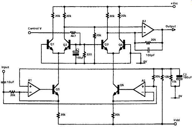
FIG. 19 Voltage controlled gain stage, due to PMI
If a step-type gain adjustment is acceptable, a simple option is shown in the layout of FIG. 20, in which the output from a point on a resistive divider chain is selected by one or other of a series of analogue switches. Since the sequential operation of these switches can be done by the use of a voltage controlled dot/bar driver IC, such as the LM3914, there would be little difficulty or expense in assembling the hardware for this type of relatively low distortion voltage operated volume control.
Digital Inputs
It has become customary for the manufacturers of compact disc players to provide a direct digital output from the disc replay, usually as the RF signal derived from the CD replay chain, shown, for reference, in FIG. 21. This RF output will usually be taken at a point following the 14-8 decoder, but before the Cross-Interleave Reed- Solomon code (CIRC) error correction stage shown in the schematic replay layout of FIG. 21. This allows the manufacturer of specialist digital to analogue signal-processing hardware to offer higher quality D/A conversion systems, more jitter-free clock regeneration circuitry (which could be very important in high precision D/A decoding), more competent error correction regimes and better anti-aliasing filtration than might be offered in a budget-priced CD player. It is argued that these latter signal handling stages probably contribute more to the overall tonal quality of the CD player than the mechanical platform itself or its control hardware.
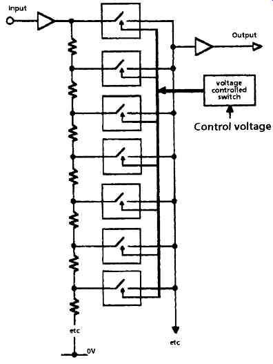
FIG. 20 Step-type gain control
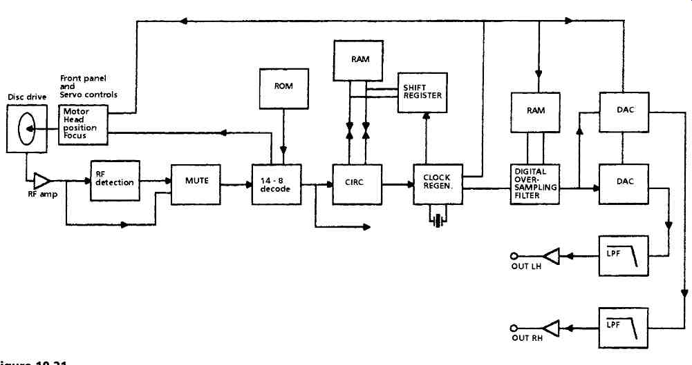
FIG. 21 CD replay schematic layout
In general, the RF output signal will be presented as a simple coaxial cable output, but sometimes in top of the range units, this signal may also be presented as an optical fiber output to avoid possible electrical interference or signal degradation in the link between the CD player and the A/D decoder.
