In the last Section I looked at the evolution of audio amplifiers, based on bipolar junction transistors, from early transformer coupled designs, having relatively unsatisfactory electrical characteristics, to comparatively sophisticated circuit layouts having a performance, both on paper and in the ears of any unprejudiced listener, which was fully comparable to that of the best tube operated designs of former years.
This, I know, will be thought to be a contentious claim by many of those who base their own technical assessments either on what they are told by those whose experience and acoustic judgements they value - perhaps because they are well known in Hi-Fi circles - or on the opinions they themselves have formed during listening trials, a complex topic I propose to consider later in this Section.
Remaining Design Problems
At the state of the art in the early 1970s, the design problems which remained- and these were only small imperfections or minor difficulties which did not usually inconvenience the user- were:
-- the need, initially, and perhaps also from time to time, to adjust the quiescent current of the output push-pull stage to obtain the best practicable performance;
-- the need to ensure that this quiescent current value remained at its optimum setting throughout the aging of circuit components or changes in junction temperatures of the transistors;
-- the need, especially in the direct coupled designs, where there was no DC blocking capacitor between the amplifier output and the loudspeaker unit, to prevent possibly damaging DC voltages appearing across the LS terminals in the event of an improper input signal or a component failure;
-- the need (since all sensibly designed amplifiers will employ negative feedback) to make sure that the stability margins of the feedback loop were sufficient to allow electrically awkward LS loads to be driven without significant waveform distortion or amplifier instability;
-- the need to evolve circuitry and components which would allow progressively higher output powers to be provided for use with increasingly inefficient LS systems. In practice, changes in outlook and expectations have meant that while a design having a 10 watt output would have been considered entirely adequate in the late 1950s, and one of 30 watt capacity quite sufficient in the 1960s, one of 150-250W output would not be thought to be needlessly over-powered in the 1990s; the need, because of a change in the majority usage of Hi-Fi equipment from classical music to various kinds of high sound-level popular styles, for all the electronically operated audio units to handle high level signal inputs without overload, or when such signal overload did occur, that the circuitry involved should handle this overload gracefully.
Power MOSFETs vs. Bipolar Junction Power Transistors (BJTs)
The major change in component availability since the late 1970s has been the growing use of power MOSFETs. The construction and general characteristics of these devices in T, D, V and U versions were explored in Section 7 (cf. FIG. 22), and some of their advantages and disadvantages were considered. Where they are used in audio circuitry, such devices are normally employed as the amplifier output transistors, almost always as a complementary, N-channel/P-channel, push-pull pair, since the electrical characteristics of these two MOSFET types are much less dissimilar than those of an NPN/PNP pair of junction transistors. However, in addition to the high- and medium-power devices, small-signal versions, mainly of T-MOS devices, are also manufactured, at voltage ratings up to 600V and current ratings up to 0.7 amperes, and permitted dissipation ratings from 300mW to 1W, in the case of the TO-237 encapsulated N-channel transistors. Similar components, though only at present at working voltages up to 450V (Vd_s), are obtainable in P-channel versions.
MOSFETs have a number of advantages and drawbacks in comparison with power BJTs. Of these the first snag is that power MOSFETs are up to three times more expensive to buy than comparable power BJTs, and the relative cost of small-signal MOSFETs may be even higher. This extra expense is mainly a function of the chip size, which determines the number of devices which can be fabricated, at the same time, on a given size wafer of single crystal silicon, and, following from this, the effects of the relative economies of scale in mass produced components. MOS devices having a low conducting resistance (RDSon) because a large number of channels have been connected in parallel, will obviously require a larger chip size, as will devices having higher working voltages - which require wider spacings between the diffusion zones. It is also claimed that MOSFETs are less linear than power BJTs when used as output source-follower pairs. However, this is only marginally true, as can be seen from the data given in TABLE 1.
Frequency Response of MOSFET Devices
The major feature of the MOSFET, which can be both an advantage and a drawback, depending on the application, is that it is very much faster in responding to an input voltage change than any BJT having comparable voltage and current ratings. One consequence of this good HF response is that, in an incompetently designed MOSFET circuit, the devices may burst into oscillation, at an extremely high frequency, as soon as the supply rail voltage is applied. Since such inadvertent oscillation may occur at a frequency which is well above the HF bandwidth of the oscilloscope which is being used to monitor the circuit, the hapless designer may only become aware that he has a problem when he finds that his output devices have become very hot and have consequently expired, for reasons which may not be apparent. The simplest answer to this particular problem is to connect a gate stopper resistor, of appropriate value (say, 150-1000~), in the MOSFET gate lead, as close as possible to the gate pin, and to ensure that the layout of the gate, source and collector leads is not such as to encourage inadvertent Colpitts, or Lecher-line-type, oscillation.
In a well-designed circuit, the MOSFET is likely to prove more robust in use than the BJT since it does not suffer from thermal runaway, and its operating characteristics are free from any secondary breakdown region, see FIG. 20 vs. FIG. 12. This saves space and expense by avoiding the need for elaborate output transistor protection circuitry.
A complementary pair of these is also, as noted above, much more truly symmetrical -- particularly at high frequencies - than an NPN/PNP pair of junction transistors. A further factor in favor of the MOSFET is that the operating current is carried by majority carriers (electrons in an N-channel device and holes in a P-channel one), and it is therefore free from the hole-storage defects which can contribute to the sluggish turn-off characteristics of any BJT, following a condition in which it has been caused to turn hard on, as might happen during a brief signal overload.
However, the major quality which endears MOSFETs to the audio amplifier designer is its high effective ff, which can be in the 100MHz region. The speed of response of any MOS device is mainly controlled by the time it takes the capacitance inherent in the gate electrode to charge up to its target voltage through the finite resistance (or current limit) imposed by the driver circuitry. (Since the channel current is controlled by the gate voltage - in an enhancement mode MOSFET, which means all the normal power devices - until this voltage appears on the gate, no channel current will flow.) This means that the designer has to hand, in the form of the gate stopper resistor, a simple tool for controlling the effective fv of the transistor. This is also true of the power BJT, but in this case the normal problem is that the fT is not as high as one would wish, rather than that it is too high.
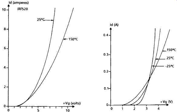
Finally, since monocrystalline silicon has a negative temperature coefficient of conductivity, MOSFETs can show a reduction in drain current for an increase in temperature- at least at larger values of drain current- and this removes the likelihood of thermal runaway under heavy load. It also implies, as seen in FIG. 1, that there will be some value of bias voltage/output current where the quiescent current setting will be nearly independent of temperature; a fact which is convenient in push- pull output stage design. I have shown, for comparison, the influence of junction temperature on the drain and collector currents of MOSFETs and BJTs in FIGs 1 and 2, and I have also, for clarity, expanded the low current region of FIG. 1 to show on a larger scale the effect of the negative temperature coefficient of the MOSFET drain current.
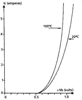
FIG. 2 Power BJT characteristics
MOSFET Linearity
One of the criticisms leveled at MOSFETs, often made I suspect by those engineers who have found experimental difficulties in obtaining stable operation, is that they are much less linear than junction power transistors, when used as output push-pull pairs of emitter- or source-followers. These claims have generally been based on the results obtained from computer circuit simulations of the push-pull transfer characteristics (cf. Self, D., Electronics World + Wireless World, May 1995, pp. 387-388), although comparisons between actual audio amplifier circuits using MOSFETs or BJTs as the output devices (cf. Toshiba, File Note X3504, March 1991) have shown the converse: that amplifier circuits using MOSFET output devices have a lower distortion than those using BJTs.
It is inevitable that any push-pull pair of devices whose input voltage/output current relationships fall short of an ideal straight-line graph will introduce some distortion into the output signal, whatever bias point is chosen, and there are big differences between the BJT and the MOSFET in this respect, as shown in FIGs 3 and 18.
These differences will influence the relative distortion introduced even by an optimally biased output push-pull pair, and I have shown the comparative results from tests using four such common circuits in TABLE 1.
========

TABLE 1 Distortion of output push-pull pair layouts
Configuration, Iq, THD (5k-ohm load), THD (10R load):
(A) Darlington pair (B) Compound E/F (C) MOSFET s-follower (D) BJT/MOSFET pair 60mA <0.02% 2.2% 60mA <0.02% 1.15% 100mA 0.02% 2.1% 100mA 0.015% 1.0%
========
Note. These measurements were made at 20kHz, at a 5V rms output voltage and a 10f~ load. The circuits used are shown in FIG. 3, and the 20kHz measurement frequency was chosen to show up any differences between nominally complementary devices due to dissimilarities in their HF response.
=========
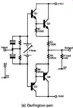
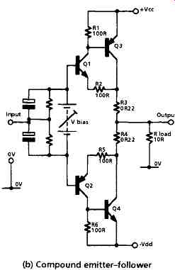
FIG. 3a/b Output push-pull pairs -- (a) Dadington pair ; (b) Compound emitter-follower

FIG. 3c/d Output push-pull pairs --- (d) BJT/MOSFET pair; (c) MOSFET source follower
The comparative measurements shown above are of the output push-pull pairs on their own, unencumbered by ancillary circuitry, and freed from any complicating effects due to the HF compensation techniques which are necessary in any feedback (voltage) amplifier circuit. The layout of FIG. 3a is that of a conventional Darlington pair output arrangement- very commonly used in solid state audio systems. That of FIG. 3b is the rather better compound emitter follower system, in which R2 and R5 have been included to make the setting of the required bias voltage rather less abrupt. FIG. 3c employs a simple MOSFET complementary-pair source follower output stage- which is in essence the same as that of the Darlington pair circuit of FIG. 3a except that because the MOSFET has a relatively high input impedance, no impedance transforming driver transistors, such as Q l/Q2 in FIG. 3a, are needed.
(For the avoidance of possible spurious HF oscillation in the circuit of FIG. 3c not only must gate-stopper resistors (R1/R4) be used, but the MOSFET source electrodes must be protected from capacitative loads. The small inductance (= 1uH) of the 0R22 wirewound source resistors serves this purpose adequately.)
The circuit of FIG. 3d is that of the compound emitter follower in which the output junction transistors have been replaced by complementary power MOSFETs. In this case gate over-voltage protection may be provided simply by connecting 10V Zener diodes across R1 and R6. I used this output stage arrangement as a recommended improvement to a previously published audio amplifier design of my own, in which I had originally used monolithic Darlington BJTs ( Hi-Fi News and Record Review, December 1980, pp. 83-85). In view of the claims for high distortion levels in MOSFET output stages, the surprising thing about the results of the trials detailed in TABLE 1 is how similar in practice the distortion levels of the BJT and the MOSFET circuits were (a factor in determining overall THD levels, as seen below). In both cases the compound emitter-follower arrangements were superior in performance to the straight Darlington pair, or the MOSFET source-follower circuit, by an approximate factor of two. A second surprising feature, observed and used by Sandman (Sandman, A.M., Wireless World, September 1982, pp. 38-39), is that with a high impedance output load (in the tests made, this would have been about 5k.Q) the residual distortion introduced by a simple emitter- or source-follower is very low indeed and, I observed, relatively unaffected by the actual Iq value chosen, over quite a wide range of settings.
To be able to obtain such a low level of crossover distortion and such an uncritical setting for the Iq value would remove one of the major problems in solid state audio power amplifiers, and this philosophy prompted Sandman to propose an audio power amplifier design in which an ancillary output circuit was used to provide a very high impedance load for the basic amplifier stage.
gm -- Values for BJTs and MOSFETs
In a bipolar junction transistor there is a predictable relationship between gm and collector current, as shown in the equation. This is only affected to a minor extent by the device geometry: gm = Ic(q/kT) where q is the charge on the electron (1.60 x 10^-19), k is Boltzmann's constant (1.38 x 10^-23), and T is the absolute temperature of the junction- giving a room temperature value for gm of 38.9S/A. In the case of both the junction FET and the MOSFET the drain current vs. gate voltage characteristics have theoretically a square-law characteristic, defined, in the case of the MOSFET, by the relationship:
Id = ( VGs- VT)=(μeC0Z)/2L
where VGS is the gate-source voltage, V T is the threshold (turn-on) voltage, ~t e is the electron mobility in the channel region, C O is the capacitance, per unit area, of the gate oxide layer, L is the channel length and Z is the channel width. This relationship can be simplified to the approximation:
gm = 1/(RDSon)
which would give a gm in the range 5-20S for a typical 100V N-channel TMOS power transistor. However, in both the JFET and the MOSFET the electrical characteristics are greatly influenced by the internal structure of the transistor- an area in which development work is continuing (c.f. the recently introduced Philips Trench-MOS devices with their very low values of RDSon and their very high and linear gm) - and most manufacturers use their control of this structure to manufacture components which are somewhat more linear than the square-law behavior predicted by the formulae.
Quiescent Current Stability in Push-pull Output Systems
The problem of setting and maintaining, once set, the optimum forward bias for a class AB or class B output stage* has been a problem with low dissipation solid state audio amplifiers ever since such things were made. There are, basically, three solutions to this problem:
-- To choose a circuit structure (such as, for example, a MOSFET complementary source-follower output pair) in which the actual value of the quiescent current is not particularly critical, so that some mid-point value can be chosen in the expectation that the resulting performance will not be too far away from the optimum; in practice, this will probably imply a fairly large value for Iq. (Typical power MOSFETs show a region on their ID/V o curves, usually for drain currents in the region 100-200mA, at which there is little change in I o over the temperature range -50C to + 150C.
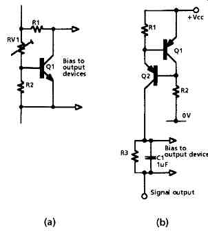
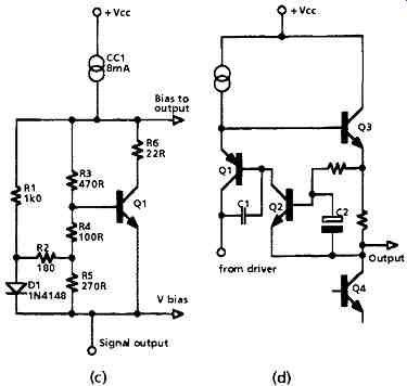
-- To use some circuit technique, such as those illustrated in FIG. 4, that will provide adequate compensation for changes in the junction temperatures of the output devices (essential in the case of bipolar power transistors) - for which proposed methods range from the simple Bailey amplified diode maintained in thermal contact with the output heatsink to the elaborate custom-built IC used by Pioneer to regulate the output device quiescent current shown in FIG. 5.
The circuit shown in FIG. 4a is a simple elaboration of Bailey's amplified diode which I used in my 1972 75W amplifier ( Hi-Fi News and Record Review, November 1972, pp. 2120-2123), while that of FIG. 4b makes use of the Williams-type constant current source built around Q1/Q2 to control the current flowing through R3, and hence the forward bias on the output devices. The layout of FIG. 4c is a further elaboration of the Bailey amplified diode arrangement, due to Self (Self, D., Electronics World + Wireless World, October 1996, p. 755), in which a further diode is used to increase its thermal sensitivity.
========
* These terms refer to the output stage biasing conditions, in that class AB operation implies that there is some residual current flow under no-signal conditions, whereas the class B designation implies that there is no such quiescent current, so that, on signal either one or other of the two output halves will be cutoff alternatively, on each half cycle of the signal, as the output signal voltage swings up or down. In practice, since this type of operation would lead to audible discontinuities around the near-zero signal regions, the vast majority of transistor operated audio power amplifiers, whose designers have sought the best compromise between quality of sound and evolution of heat, will operate in class AB.
FIG. 4 Output stage bias systems.
Other Iq Control Techniques
A number of circuits have been proposed in which the emitter/collector currents of the output transistors are monitored, and used to regulate the forward bias voltage so that the desired quiescent current is held to some constant value. In general, this type of control arrangement is only satisfactory with a system biased into class A operation, such as that described by Nelson-Jones (Nelson-Jones, L., Wireless World, March 1970, pp. 98-103), and shown in FIG. 4d. Even then, a large value capacitor (as C2 in the diagram) is needed to remove the low frequency signal components from the Iq control voltage.
In all cases where BJTs are used as the output devices it is essential that the sensing transistor (Q 1 in the diagrams of FIG. 4) should be in as close thermal contact with the output transistors as possible. Self even proposes gluing the sensing transistor to the case of one or other of the output transistors (Self, D., Electronics World + Wireless World, May 1996, p. 412) in an attempt to reduce the time lag between the output transistor heating up during a high signal-level program passage - which will cause an increase in the output quiescent current of the BJTs -- and this temperature increase being sensed, or the corresponding time lag between the output BJTs cooling down again, during a quiet passage in the program--which will reduce their quiescent current setting - and the sensing transistor registering this change in heat evolution. Of these two periods of discontinuity between the output transistors heating or cooling and that fact being registered by the sensing transistor, it is the second which is more important to the performance of the amplifier since the nature of the crossover distortion- particularly in a BJT output stage - becomes less acceptable at quiescent current settings below the optimum value.
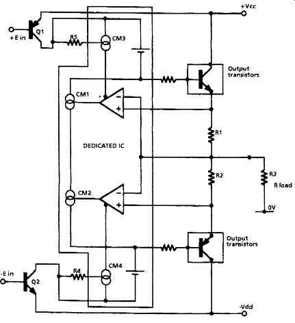
FIG. 5 Pioneer Iq control circuit
In the Pioneer M-90(BK) 250 watt amplifier, which has groups of eight parallel-push- pull connected BJTs in the output stage of each channel, a purpose-built IC, having the circuit layout shown schematically in FIG. 5, is used to sense the temperature of the amplifier, the quiescent current of the output devices and the signal level, and to anticipate and control variations in the quiescent current setting of the output devices.
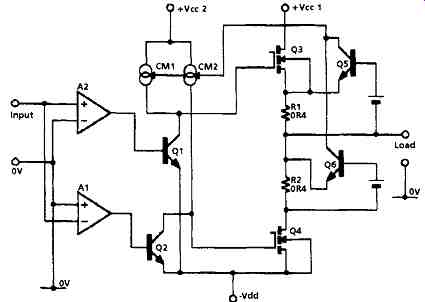
A further system for quiescent current control in an output pair of current driven MOSFETs was proposed by Van de Gevel (Van de Gevel, M., Electronics World + Wireless World, February 1996, pp. 140-143), and is shown, in greatly simplified form, in FIG. 6. In this the source/drain current of the output MOSFETs (Q3/Q4) is converted into voltages across R1 and R2, and these voltages are compared with fixed reference voltages by Q5 and Q6. The sum of these voltages - converted into a current by Q5 and Q6- is then used, via the two current mirrors, to modulate the collector currents of Q1 and Q2, and hence the bias voltages applied to the output MOSFETs. The purpose of this arrangement is that the effect of input signals which are applied differentially to the output devices is partially cancelled by subtraction, and is not used to diminish the Iq level, whereas those changes which occur in both devices (i.e. due to changes in static Iq) are added in the control system. It is claimed that this also has the effect of ensuring that neither output transistor can be cut off at any point of the input signal.
However, although the preceding circuit layouts partially solved the problems of variable quiescent current and the need to set this, at least once, during manufacture, or use, it still did not provide a design basis for an amplifier which required no setting up. The first really satisfactory circuit arrangement which remedied this problem was introduced in 1975 by the Acoustical Manufacturing Co. (Quad).
The Quad Current Dumping Amplifier
The circuit layout of this amplifier is shown, in its essentials, in FIG. 7, and its intention is to allow the output transistors (Q1,Q2) to be operated at zero bias and zero quiescent current- a condition which requires no initial setting-up adjustment. Its operation can be considered to lie in either one or other of two distinct modes, that when the output transistors are non-conducting, and that when the output transistors are in their normal operating condition.
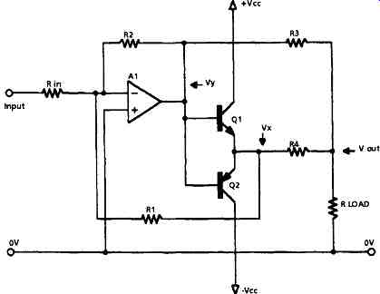
FIG. 7 Current Dumping circuit
Taking the first of these first, a low distortion small power amplifier, A1, is arranged to drive the load through R3. Since there is in this operating mode no contribution from the output transistors, the signal returned to the input of A1, through the main feedback loop (R1/Rin), will act to hold the output signal (Vout) to the level determined by the feedback signals through (R1 + R4)/Rin, and R2/Rin, and, provided that the required load currents are within the capability of A1, the overall system will operate with very low distortion.
However, if the signal output level at Vy is increased to the extent that one or other of the output transistors is driven into conduction, the voltage at Vx, and hence the current through R4 into the load, will be increased, thereby increasing the amount of NFB through R1 to the input of A1, and reducing the gain of A1 to compensate for the added gain of the output transistor which is now in circuit. If R4, R2 = R1, R3 then the extent to which the gain increases or is reduced, as the output transistors pass into or out of conduction, will be exactly compensated by changes in the amount of overall NFB which is applied, and there will be no crossover distortion introduced by the unbiased output devices.
So far, so good. The arrangement proposed by Quad provides a simple and readily understood means of using unbiased output transistors without a major penalty in respect of the system distortion. Unfortunately, the presence of R4 in the output signal path to the load would lead to an undesirable waste of output power, so Quad replaced R4 with a 3.3uH inductor (Z4) and preserved the equivalence of R1, R3 = Z4, Z2 by replacing R2 with a 120pF capacitor (Z2). Though this exchange preserves the intrinsic philosophy of the design it made the actual operation of the amplifier significantly more complex, which allowed those of the Hi-Fi press who resented Quad's aloof approach to outside reviews a pseudo-technical reason for denigrating the performance of this remarkable design.
The Sandman Class S System
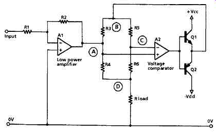
As is shown above, in TABLE 1, all of the simple push-pull output layouts shown in FIG. 3 exhibit a conspicuous reduction in their levels of distortion when their normally low impedance output load is replaced by a high impedance one: a reduction in distortion from 1-2% down to less than 0.02% being typical. This effect was noted by Sandman, who proposed the circuit shown in FIG. 8 (Sandman, A.M., Wireless World, September 1982, pp. 38-39). The way this circuit works is that a low power, very linear amplifier, A 1, is arranged to drive the load through R4, while a high power, low quality amplifier is used to drive the bridge network R3-R6 at point B, and, through this, the output load. The voltage comparator, A2, monitors the extent of the bridge unbalance, and drives the output transistors so that the current fed into the resistor bridge at point B ensures that the difference in voltage level between points A and C is very small. By making the signal voltage developed across R4 very small, the high power devices effectively present the small power amplifier with an infinite impedance load. Some crossover effects will, of course, arise during the period in which the base voltage applied to Q1 and Q2 is swept across their non-conducting regions. During this brief excursion A 1 will supply the load directly through R4. The resistor values used in the bridge should be low enough to allow this.
The Technics Class AA System
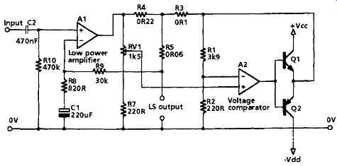
This arrangement is shown in FIG. 9, and is used in the Technics SE-A 1000 power amplifier and all their current power amplifier designs. This circuit has obvious similarities in its approach to the Sandman design, and clearly uses the same basic philosophy in which an output push-pull power amplifier (they call this a class AA stage) operates to provide a very high impedance load on the voltage amplifier. The Sandman/Technics approach offers a unique and valuable way of reducing overall amplifier distortion without requiring high loop gains in the power amplifier, or thereby reducing the loop stability margins.
Voltage Amplifying Stage Gain and Overall THD
In normal amplifying systems employing NFB the open loop gain (i.e. before NFB is applied) will be made as high as feasible- so far as this is possible without introducing an unacceptable level of loop phase error- so that there will be enough gain left over to allow a useful amount of NFB to be applied. The relationship between distortion and negative feedback is:
D' = Do /(1 + β Ao)
where D ~ is the distortion before NFB is applied, D' is the harmonic distortion after the application of negative feedback, 13 is the feedback factor (by which I mean the proportion of the output signal which is fed back to the input) and Ao is the open loop gain of the amplifier. This is very similar to the relationship between closed loop gain and negative feedback:
A' = Ao /(1 + β Ao)
where A ~ and A" are the respective values of the stage gain before and after the application of NFB. The implication of these two equations is that the distortion is reduced in direct proportion to the reduction is stage gain. However, the relationship is only an approximate one since the presumption is made, in the case of harmonic distortion, for example, that the amplifier gain (and the feedback factor) remain constant as a function of frequency from that of the fundamental to that of the nth harmonic--an assumption which is unlikely to be true, and which is the major reason why the distortion of an amplifier with NFB will worsen as the frequency is increased.
It also makes the assumption that the feedback remains negative throughout the frequency range of interest, which may be only marginally correct.
However, if we assume for the purposes of this argument that the distortion is reduced in the same proportion as the gain, and that the closed loop gain is the product of the open loop gain and the feedback factor- which will be nearly true if the gain (A ~ is very high- then for an amplifier with an open loop gain of 1000", to which NFB has been applied to reduce the gain to 10% if the initial distortion (D) was 2%, then the distortion with NFB applied (D') will be 0.02%, and this is the basis of the design for almost all the commercial audio amplifiers on sale in Hi-Fi shops, for which the two performance factors of greatest interest to the (probably naive) purchaser are the total output power and the total harmonic distortion. So far as the THD is concerned this is mainly determined by the amount of NFB which can be applied, which, in turn, depends on the open loop gain which can be obtained from the voltage amplifier stage.
This is a function of the circuit structure which is used, and I have shown how the gain can be increased by refinements in the circuit layout in the various diagrams of FIG. 10.
Basic Gain Stage Constructions
All of the gain stages I have shown are based on the long-tailed pair circuit configuration- sometimes called a differential pair- because this allows the signal to be operated upon between a symmetrical pair of supply lines, and permits the design of amplifiers which do not need a large value output DC blocking capacitor- a component disliked by the Hi-Fi aficionados because of its supposedly variable and voltage dependent characteristics- and is therefore the approach used in all audio amplifier designs having any pretensions to high audio quality. The test conditions for all the circuits were: frequency 1kHz, supply voltage +15V, 3V rms output.
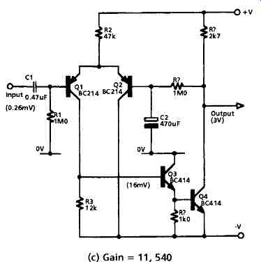
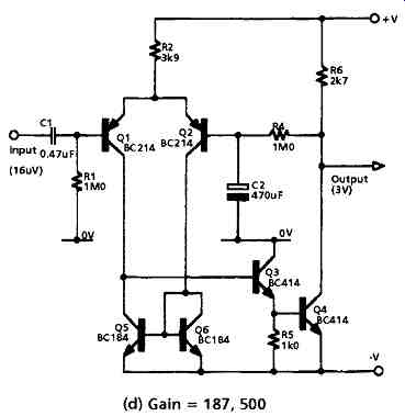
In the layout of FIG. 10a, 100% DC negative feedback is applied through R4 and C2 to stabilize the output DC potential, which is held to 0V • but, because C2 shunts the AC component of the feedback signal, allows virtually the full AC stage gain (A ~ to be achieved. The current through both Q1 and Q2 is about 2mA. This relatively high value is commonly chosen to increase the slew rate of Q3, between whose collector and base a dominant lag HF stabilizing capacitor of 50-100pF (not shown) will normally be connected. Because of the need to ensure similar working conditions for both of the two input transistors R2 must be chosen to provide a voltage drop of about 0.6V at a current of 2mA, which requires an inconveniently low value for this component from the point of view of stage gain, which, in the circuit shown, is 4412". Elaborating the circuit so that Q3 becomes a Darlington pair, Q3/Q4, as in FIG. 1 lb, allows R3 to be increased to 680R, and this, predictably, very nearly doubles the stage gain to 9091 ". Since R3 is still a low value, the benefit offered by the relatively high input impedance of the Darlington pair cannot be utilized. If the need to keep the slewing rate of Q3/Q4 as high as possible can be ignored - perhaps by the use of a different method of HF loop stabilization - the input transistor currents can be decreased and R3 increased to 12k, which will increase the stage gain to 11,540". A much more profitable approach would be to replace the load resistor of Q 1 with a constant current source which would offer a dynamic impedance at least ten times greater than a 680 ohm load resistor, giving a stage gain increase to some 100, 000 ~.
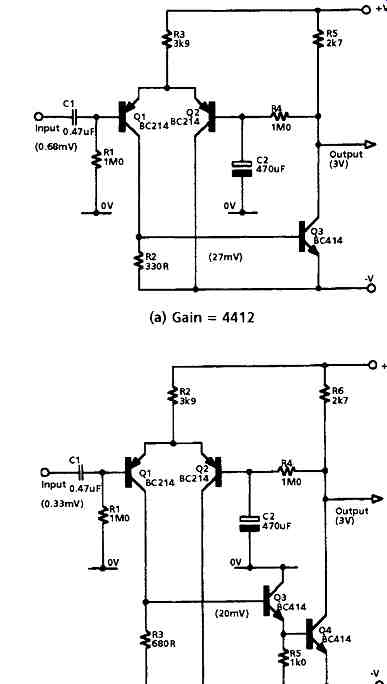
FIG. 10a/b Simple gain stages. (a) Gain = 4412; (b) Gain = 9091
Even better, and using no more components than a typical constant current source, would be the use of a current mirror, as shown in FIG. 10d, which combines the outputs of Q1 and Q2 and will double the gain given by a simple constant current source, to provide a measured stage gain of 187, 000". Ideally a matched pair of transistors should be used for Q5 and Q6 (or, indeed one of the proprietary IC style current-mirror devices, available in various input/output current ratios). Failing this, a low value preset potentiometer should be inserted in the mirror transistors' emitter leads, as shown in FIG. 10e, to allow the currents through the two input transistors to be balanced.
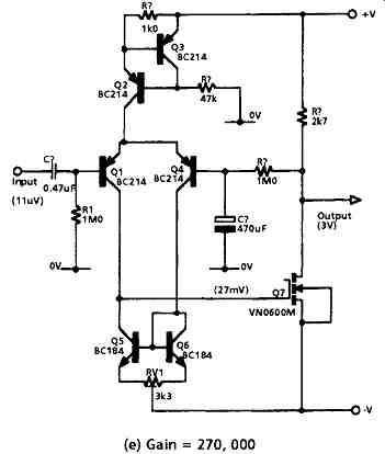
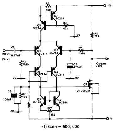
A practical snag with all of the circuits shown so far is that they offer very little rejection of any intruding signal voltages present on the +ve supply rail, and this would inevitably degrade the circuit performance. Substituting a two transistor constant current source for R2 in the earlier designs would avoid this problem, and possibly also allow a small further increment in stage gain. In the circuit diagram of FIG. 10e I have also explored the use of a small-signal T-MOSFET, which is very linear in use as a class A gain stage, and also has a very high input impedance. This increases the gain still further to 270,000". A final beneficial circuit refinement, shown in FIG. 10f, is to insert a pair of cascode connected transistors (Q3 and Q4) in the collector circuits of the input transistors. This has the effect of clamping the collectors of Q1 and Q2 to a fixed DC voltage- approximately 4.5V -- so that there is no effective negative signal feedback through the internal resistance and capacitance between collector and base of Q1 and Q2, and avoids any loss of gain in the input transistors due to this unwanted internal feedback. With this refinement the circuit gain is increased yet further to 600,000". In all the circuits I have shown so far I have used a simple 2.7k resistive load for the output, although it would clearly be possible to obtain a considerable increase in unloaded stage gain if the output load resistor were to be replaced by, for example, a high dynamic impedance constant current source. This choice of load is quite deliberate, in that the circuits explored have all been of a kind which could be used in the gain stages of an audio amplifier, where the output stage would be a push-pull pair of Darlington connected emitter-followers or a similar pair of complementary MOSFET source followers, for which, I felt, a 2k7 ohm resistor, with the possible addition of a 2000pF shunt capacitor, would be a more representative type of gain stage load. In any practical audio amplifier, the gain stage would be operated with a high dynamic impedance load in order to increase the extent of supply-line signal rejection, but this would not increase the open loop signal gain because of the loading effects of the output devices.
Output-Input Signal Isolation
In most real-life amplifying devices there will be a signal feedback path from output to input, and in a transistor the capacitative component of this will depend on the junction area and the collector to base voltage. For a typical junction transistor of 1W dissipation and 50V V c, this feedback capacitance (Cc_ b) will be will be in the range 5-10pF, while for a comparable small-signal MOSFET, Cd_g will be about 30-50pF, and the Miller effect due to this feedback capacitance will reduce the gain at higher signal frequencies. This loss of HF gain can be lessened by cascode connecting the output device, as I have shown in FIG. 11. This somewhat reduces the 1kHz gain to 330, 000, but allows a gain of 90,000 at 20kHz, by comparison with the circuit of FIG. 10f, which has a gain of 600,000 at 1kHz, but only 30,000 at 20kHz. This is not an additional problem with most conventionally designed audio amplifiers, since in these a capacitor in the range 50-100pF will be connected between the collector and base of the device to cause a feedback stabilizing dominant lag, but if some alternative method of loop stabilization is to be employed, an output cascode connected buffer could be valuable.
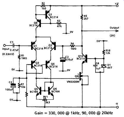
FIG. 11 Cascode output isolation -- Gain = 330, 000 @ 1kHz, 90,000 @ 20kHz
Effect of NFB on Signal Distortion
If an open loop gain of 90,000 is available, and the required gain, with feedback, is 30, then a factor of 3000 is available to reduce the distortion of the amplifier. If we assume that the distortion of an output pair of emitter-followers worsens from 2% to 20% as the amplifier output approaches its overload point, then the (theoretical) residual distortion, near overload, could be reduced from 20% to 0.006%. This is a somewhat artificial assumption since there are a number of other factors which will degrade the overall distortion figure, such as the unsuspected generation of signal voltages between points which are notionally at the same potential, or the failure - seen above in some tube amplifier designs - to derive the feedback signal from the point at which the LS load is connected. However, I am left with the feeling that designers who claim THD figures of the order of 0.0001%, or even 0.001%, are talking about the predictions drawn from simplistic computer simulations rather than the actual performance of real pieces of hardware. There are, of course, techniques, such as those suggested by Sandman, by which the distortion of the output stage can be reduced without relying entirely on the improvements brought about by NFB, and these would result in a genuine improvement in results, but these are an exception to the normal practice of commercial audio power amplifier design.
Symmetry in Gain Block Structure
A range of well-known solid-state gain stage layouts has been shown above and in previous Sections, and it is clear that the contemporary audio amplifier circuit designer-- unlike his predecessors in the days of tube circuitry- has a very wide choice of component arrangements at his disposal. So far as there is any general trend in contemporary audio amplifier design it is towards the completely symmetrical type of layout such as that due to Borbeley and shown in FIG. 12 (Borbeley, E., Wireless World, March 1983, pp. 69-75). The basic structure of each half of this circuit is similar to that of FIG. 10c with the added refinements of an output cascode buffer between Q4 collector and the output load, and with a constant current source in place of R2. Because the system is fully symmetrical, and employs active loads (Q10/Q11) the 1kHz stage gain, at 30, 000 ~, is twice that which would be given by the equivalent single-ended layout of FIG. 10c.
The basic aim of this circuit structure is to lessen or eliminate the inevitable effects of slew rate limiting which will occur under limiting conditions in any single-ended system. This purpose is assisted by the stabilization of the feedback system by the use of a pair of HF step networks (C2/R10, C1/R6) which do not begin to limit the HF gain until 72kHz, which is well outside the 22kHz design bandwidth determined by R18 and C4. My own judgment is that this type of layout is much superior to the dominant lag stabilized designs of the type shown in FIGs 10c or 10d, which typify so many of the middle-Fi offerings of the present day. This view is obviously shared by a number of major Japanese audio equipment manufacturers who have adopted the essential features of Borbeley's circuit design.
Negative Feedback and Sound Quality
Although it is possible, in principle, to design an amplifying module which exhibits progressively smaller amounts of steady-state harmonic distortion, by the use of negative feedback connected around a gain block of increasingly high gain, there is no guarantee that the amplifier module so made will be satisfactory in use in any given audio application. I will explain.
I feel, sometimes, that it is a pity that audio amplifying and sound reproducing equipment succeeds or fails depending on the reactions it evokes in the ears of those who listen to it. My misgivings arise because the characteristics of the human ear vary from person to person, and from day to day, and since what is heard by the listener is subject to his personal dislikes or preferences, the acoustic performance of the equipment cannot be completely specified, with certainty, by any set of electrical or engineering specifications. One can make guesses that certain features of the design will be a good thing, or that certain other features which one has tried to avoid or minimize would have been bad things, but one can never do better than feel confident that what one proposes or has made will be favorably judged by one's peers.
It is because of this that those electronics engineers who have designed audio amplifiers and other signal handling equipment, which has been judged by their users to perform to their entire satisfaction, enjoy a higher seat in the electronic engineering Pantheon - because of some supposed mastery of the black arts of audio - than other equally competent engineers who had designed, for example, instruments to tell a submarine captain how far he is beneath the surface of the sea, or who has designed, say, a simple, efficient and reliable mechanism for opening and shutting the hatches which enclose the landing gear on an aircraft.
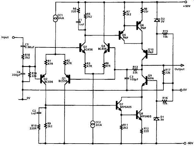
FIG. 12 Borbeley symmetrical driver
Certain aspects of audio design can be specified with relative ease - such as the power bandwidth, the uniformity of the frequency response over the audio band between, say, 10Hz and 20kHz, the output power which can be delivered to certain specified load impedances at certain levels of distortion, the size of the input signal required to produce the specified output power, and the signal to noise ratio of the equipment or the signal breakthrough from one channel to another, in a stereo or multi-channel system- however, all of these measurements relate to purely steady state characteristics, such as could be made with an input signal derived from a low distortion, constant amplitude, variable frequency sine wave oscillator, and bear only a fleeting resemblance to the nature of the audio signals which are likely to be presented to the equipment. These will consist of a multiplicity of simultaneous signals, each having widely variable amplitudes and rates of change of amplitude, and most of these waveforms will be non-repetitive quite unsymmetrical.
The task of designing a signal source which would simulate all of the relevant aspects of an audio signal in demonstrating equipment shortcomings is a daunting one, but quite a lot of information - particularly that relating to poor loop stability in amplifiers using NFB - can be shown by the use of an input square-wave signal, as I have illustrated in Fig 12a to 12g, in my book Audio Electronics (Butterworth-Heinemann, 1995, pp. 280-284). Much more needs to be known and specified in relation to any audio amplifier before it can be declared to be satisfactory, but, at the very least, no statement of performance can be regarded as complete without the illustration of the performance, as demonstrated by real-life hardware, under test on reactive loads, photographed on the screen of a wide-bandwidth oscilloscope. This is relevant because this is the area where the inadequacy of HF feedback loop compensation methods will show up - both on the oscilloscope screen and in the ear of the listener. As a supplement to the oscilloscope waveforms, it would be valuable to specify the output square-wave settling time of the system, for various test frequencies, amplitudes and load characteristics, defined as the time required, in microseconds, for the output waveform to settle within +1% of the required output level, following an input step-function-type change of input signal level, as shown in FIG. 13.
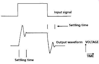
FIG. 13 Amplifier transient response and settling time; Input signal: Settling
time; Settling time, Output waveform, VOLTAGE vs TIME
Power Amplifier Output Stages
Although for a time it seemed that the undoubted advantages offered by power MOSFETs as output devices- greatly extended HF gain, freedom from secondary breakdown (allowing simpler methods for output transistor protection), greater intrinsic stability of the DC working point, greater ease of paralleling output devices to allow increased output power, as shown, for example, in the output layout of the Borbeley design, illustrated in FIG. 14- would ensure a growing number of MOSFET based audio amplifier designs, the major mass-market manufacturers continue to use bipolar power transistor layouts of the general form shown in the Marantz PM-16 design of FIG. 15. In this circuit, the forward bias for the required output transistor quiescent current is generated by a simple amplified diode layout built around a monolithic Darlington transistor pair (Q7/Q8), the output transistor overload protection is provided by the simple Zener diode chain across the signal input to Q 1 and Q6, and output LS protection is given by a relay cut-out whose contacts (not shown) are situated in the LS output line.
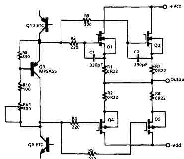
FIG. 14 Borbeley output layout
The most notable feature of this power amplifier design (whose output is rated from 90 to 150W per channel, depending on the output load) is the elaboration of the normal output complementary Darlington pair into a symmetrical three-transistor cascade (Q1/Q2/Q3 and Q6/Q5/Q4). The cross-coupling of the driver transistor emitter circuits, via R6 and R3/C1, is now quite conventional practice for the driver stages of power junction transistors since the reverse biasing of the output transistor base circuits helps drain the stored holes from the base-emitter region and thereby speeds up the turn-off time of the transistor following any period in which it has been driven momentarily into saturation.
A virtually identical output configuration--following a Borbeley-style symmetrical driver stage--is used by Rotel in their RHB10 200-330 watt power amplifier, though in this, the output transistors Q3 and Q4 in FIG. 15 are replaced by four parallel connected devices as each half of the output emitter-follower pair, current sharing being ensured by the inclusion of a separate 0.22 ohm emitter resistor and a 10 ohm base resistor for each transistor. Once again, the input bias needed to establish the output quiescent current is achieved by a simple amplified diode, and output LS protection is afforded by a relay cut-out whose normally closed contacts are located in the LS circuit.
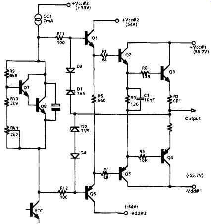
FIG. 15 Marantz PM-16 output layout
Output DC Offset Control
Almost all contemporary audio amplifiers are based on the split-supply rail philosophy, in which the input-output signal path operates about a zero mid-point voltage, and the output of the amplifier is connected by a DC path to the LS output terminals. This type of circuit layout demands that there shall be no significant (say, not greater than 10mV) DC offset present across the output terminals, and this is now achieved, almost universally, by the use of an op amp in the input signal path as shown in FIG. 16, since most off-the-shelf op amps will have an intrinsic DC offset within a few mV, even without any adjustment. Unfortunately, this type of offset removal, though effective and inexpensive, brings with it the problem of switch-on plop, since it is certain that the voltage required at the inverting input of A1, for zero DC offset at the power amplifier output, will not be zero, and until the capacitor C1 has charged to the required voltage through R4 there will be an unwanted amplifier output voltage.
The longer the time constant of R4 and C1, the longer this error voltage across the LS load will persist, and the time constant cannot be shortened without impairing the amplifier LF gain.
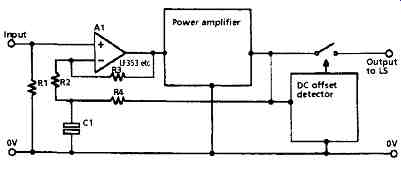
FIG. 16 DC output offset control
If there are relay operated switching contacts in the LS line, as shown in FIG. 16, used to protect the LS load from any circuit failure which would generate a damaging DC offset at the LS output terminals, then this relay circuit can be used to isolate the LS from the amplifier output until there is zero residual DC present at this point following switch-on. The effectiveness and simplicity of this method has resulted in its widespread adoption among commercial systems. However, these switch contacts may have to handle high output currents in use, so very good quality switching contacts are essential if signal degradation is to be avoided.
Hybrid Systems
A number of hybrid systems have been proposed, such as that by Mortensen, using tube driver stages and MOSFET outputs (Mortensen, H.J., Audio Amateur, January 1989, pp. 14-20) or Macaulay, using transistor driver stages and pentode tube outputs (Macaulay, J., Electronics + Wireless World, October 1995, pp. 856-859), intended either to take advantage of the robustness of transformer-coupled tubes in respect of overload, or the freedom from the need to use an output transformer offered by low output impedance solid state designs, but these ideas seem to have had negligible impact on mainstream circuit design which, apart from what I consider to be the hunting grounds of wealthy eccentrics, has remained unshakably solid state.
Listening Trials
The purpose of Hi-Fi magazines is to sell Hi-Fi magazines, and, in the process, to make money for their publishers, to give employment to their staff and to provide entertainment and instruction for their readers. In this respect they are no different from any other periodical, with the possible exception that their contributors must deal, to a significant extent, in informed opinion rather than in simple statements of fact, and this aspect of their editorial content comes very much to the fore in their judgments of audio amplifiers, since the basic specifications of so many of these are so similar that a judgment by the potential purchaser, solely on the basis of specified performance, would be very difficult. Because of this, there has been a growth in the numbers of reviewers who have made a specialty of the assessment of the quality of the sound produced by any given audio power amplifier (or, to a lesser extent, preamplifier) when it is used to reproduce any particular piece of music.
Inevitably, personal preferences on the part of the reviewer, in respect of the styling or convenience of the equipment, or the general helpfulness or generosity of the manufacturers, must, with the best will in the world, spill over into the area of the reviewer's technical assessment of the performance of the unit, and the reviewer's judgment of its tonal quality. This may not matter very much to the average reader, who is probably unlikely to want to buy that particular product anyway, and may quite enjoy reading slanging matches between august names, but it is a matter for considerable concern for the manufacturers who may feel that their products are being unfairly denigrated by a coterie of prejudiced or hostile reviewers, or by engineers who feel that the wrong lines of technical development are being extolled. For this reason, both the manufacturers (to defend their products from unfair attack) and the magazines and their reviewers (to establish in the eyes of their readership their ability to make valid subjective judgments) have, from time to time, set up comparative performance trials in which panels of listeners have been invited to record their preferences for one or other amplifier or other piece of equipment, which should, ideally, be randomly selected by a third party- or, indeed, by some electronic sampling mechanism without any human interest in the proceedings or their outcome.
An early comparative trial along these lines was commissioned by Quad, and reported by Moir (Moir, J., Wireless World, July 1978, pp. 55-58). In this trial, individual members of a panel of six skilled jurors, mainly drawn from those having an engineering involvement in sound reproduction, were asked to express their individual preferences for one or other of a pair of units presented anonymously in randomly ordered sequential tests. These tests could be between different amplifiers or (as a check on the panel's ability to distinguish similarities) between the same unit twice repeated. The units compared were Quad II tube amplifiers, Quad 303 transistor amplifiers, and the Quad 404 Current Dumping power amplifier- a unit which does not seem to have been fairly treated by the young cognoscenti of the Hi-Fi press. When the results of this carefully prepared and executed trial, which involved some 373 individual tests, were subjected to statistical analysis the results indicated that, in the judgment of the panel, there was no obvious and significant preference for one unit rather than another, and that the members of this highly skilled listening panel were generally unable to distinguish one unit from another.
The results of the Quad trial were so clearly at variance with the long-term experience and expectations of the Hi-Fi press or their contributing reviewers that a repeat trial was organized by Martin C. and Hi-Fi News (HFN/RR November 1978, pp. 110-117), and reported on by C. and Adrian Hope. The purpose of this repeat trial, with a initial judging panel of seven members, largely drawn from the Hi-Fi press, was to try to eliminate the possible factors which might have blurred the distinctions between different systems, a confusion of outcome which the critics felt must have occurred in the trials sponsored by Quad. This second trial employed a Quad 405, a Naim NAP 250 and a TVA Export (high power tube operated) amplifier-- and so embraced a wide range of technologies as well as a wide spectrum of popular esteem. In the event, the results were remarkably similar, in that, with two exceptions, the (again highly experienced) panel was unable to differentiate between the units under test.
Since great care and self-control had been exercised by the members of this panel to avoid influencing each other's judgments it was surprising to discover that there was obvious evidence of cross-influence in the results. However, ignoring this discovery, which did not, in this case, affect the results, the outcome was largely the same as that from the Quad trial, that the panelists were, as a whole, unable to decide which unit they were listening to, or whether any one unit was superior to another. Once again, it was felt by C. that the outcome was, in some way, distorted, perhaps by the very large number of musical excerpts to which the panel had been asked to listen or the relatively short length of each trial, so the tests were repeated, with a larger (13 member) team of jurors, who were asked to adjudicate on their own, and were allowed to increase the duration of each trial as wished. Once again there was no clear evidence that there were audible differences between the units under test, apart from the suggestion that two of the panelists were able to identify individual amplifiers, perhaps because of small residual differences in their frequency response.
Speaking for myself, as an amplifier designer who listens to the results given by his designs, I know quite well that there are audible effects which result from various identifiable and measurable electrical design defects, and measurements on those commercial designs to which I have had access have frequently revealed the presence of uncorrected electrical defects of kinds which I have learnt to associate with certain faults in sound quality. However, even when one has trained one's ears to recognize these faults, this recognition may take a little while.
At this point, may I introduce Fingal, my Siamese cat, who had a great liking for Bach organ music, and would climb onto my lap, and purr contentedly whenever I played one of his favorite pieces from gramophone record. If I had made any change in the reproduction system he would be aware of this, and signify his awareness by the angle or alertness of his ears. If, after a minute or two, he was prepared to accept the change he would settle down to (apparently) enjoy the music. On one occasion I was lent, for lecture purposes, an expensive and impeccably specified Hi-Fi amplifier. As soon as I began to play music through this new system Fingal leapt from my lap and fled from the room. Actually, I agreed with his judgment.
My conclusion, clearly shared by Fingal, is that there are audible differences between amplifiers, but, between good units, the differences are small, and not always easy to identify in a short listening session. I also believe that most of the more experienced Hi-Fi reviewers are sensitive to these differences, but tend greatly to exaggerate their importance. In my experience there are greater differences between the sound of comparable LS units, or phono cartridges, or even CD players, mainly for clear and identifiable and measurable reasons. As engineers become better at identifying and minimizing measurable faults, then also these differences will diminish.
