The concept of feeding back into its input some part of the output signal from an amplifying block was invented, like so many other useful ideas in the field of electronics, by Major Edwin Armstrong, of the US Army Air Corps. His initial intention was to use positive (i.e. signal level enhancing) feedback (PFB) to make the electrical oscillators which were required as signal sources for radio broadcasts, but it was soon discovered that the feeding back of an antiphase signal - signal diminishing or negative feedback (NFB) - from the amplifier output into its input circuit also conveyed some valuable advantages. In particular, simple NFB can reduce the extent of any waveform distortion or noise introduced by the amplifier block, and can help to make the frequency response of the system more uniform.
I describe this usage as simple NFB because there are many other circuit possibilities using NFB in which the feedback is used to cause specific modifications to the frequency response characteristics of a circuit block, as, for example, in the construction of frequency response correction circuitry or notch or bandpass filters. These will be considered later.
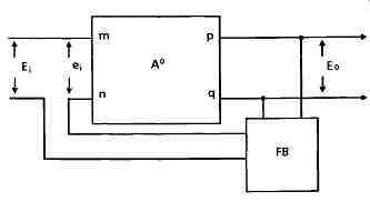
FIG. 1 Layout of feedback system
The effects caused by the normal - flat frequency response - type of voltage feedback are most easily explored by reference to the simple schematic layout shown in FIG. 1. In this a circuit block having separate, and isolated, input and output connections, m-n, p-q, and a gain of A ~ is connected so that a proportion of the output voltage is fed back, in series with the input signal, Ei, through a network, FB, having a gain of 13. If we define the signal actually appearing between the input points m-n as e i, and that appearing across the output points p-q as Eo, then the stage gain of the amplifying block, Ao, is:
Ao = Eo/ei (1)
which is called the open loop gain- i.e. the gain before any feedback is employed.
However, if the electrical network, FB, connected between the output and input of this gain block causes a proportion 13 of the output signal to be inserted in series with the input voltage Ei, then the actual input applied to the gain block will be changed, so that e i will actually be Ei + ~Eo, or
Ei = ei – Beta Eo (2)
These equations allow us to determine the effect of feedback on the stage gain, bearing in mind that in the absence of any feedback signal, Ei = ei.
The closed loop stage gain, i.e. that when feedback is applied, is normally called A', and is defined by the equation
A’ = Eo/Ei (3)
Combining equations (2) and (3)
A’ = Eo/(ei – Beta Eo), but ei - Eo/A0 therefore …
One of the effects which can be seen immediately from equation (4) is that, if the feedback is positive, then if Beta Ao is unity, the stage gain will be infinite. This consideration is important for two reasons:
-- that if there is some mechanism in an electrical circuit which limits the gain once a certain output amplitude is reached, then the use of positive feedback can be made to provide a continuous and stable amplitude output signal from the circuit without any input signal being required. In general, some frequency determining network will be employed to ensure that this output oscillation occurs at some desired and specified frequency;
-- that if there is some characteristic of the layout or the components used in the gain block which tends to cause a phase shift in the fed back signal, so that, although the feedback factor Beta is intended to be negative, it is actually positive at some frequency, then continuous oscillation may occur at that frequency if the closed loop gain reaches unity. Not only that, but the stage gain will tend to increase, in any amplifier employing negative feedback, where the phase shift of the fed back signal causes this to be positive, even though the amount of the feedback may not be enough to cause oscillation.
There are a number of advantages and disadvantages which are inherent in the use of feedback in an amplifying system, and it is essential, in any design, that its designer should be aware of the latent problems as well as the required benefits.
Benefits of Negative Feedback
If the feedback network (FB) is a phase inverting one, so that Beta is negative, then the gain equation will be:
A'= Ao/(1 + Beta Ao) (5)
In this case the closed loop gain will decrease as the amount of feedback is increased, up to the point at which Beta Ao is so much greater than 1 that the equation approximates to:
A'=Ao / Beta Ao or A'=1/Beta (6)
This relationship is of particular interest where A ~ is very high, because in these cases the gain with feedback, A', is almost completely determined by the attenuation ratio, 13, of the feedback network, so that if Beta is 1/10 then the gain A" will be 10, and if Beta is 1/100, then the stage gain will be 100, and so on. This is a valuable feature in the case of tube amplifiers, or other circuits where the performance of the components may be expected to deteriorate with time, in that it will sustain the gain and other qualities of the circuit in spite of component deterioration.
Some further valuable features can be predicted, particularly in the limit case where A’ tends towards 1/Beta, for example that, if the feedback network has an attenuation which is independent of frequency, then the action of the feedback will be such as to make the amplifier gain also independent of frequency. Also, if the feedback network is distortion free, then, if the gain (Ao) is high enough the output will also be distortion free. A logical deduction from this is that, for those cases where Ao is less than infinite in value, the distortion (Do ) of the output signal will be reduced in direct proportion as the value of Beta Ao increases, giving the relationship
D' = Do(1 + Beta Ao) (7)
…where Do is the distortion without feedback. However, this relationship makes the assumption, not always found in practice, that the open loop gain (Ao) is still sufficiently high, and negative, at the frequencies of the various higher harmonic components which go to make up the total distortion. A similar prediction can be made about the reduction of 'hum' and noise introduced by the amplifier block, provided that the feedback network is itself hum and noise free. This feature is particularly valuable in tube operated audio amplifiers, since the poor smoothing of the HT+ supply lines, and the likely induction of hum, from external AC fields, into the windings of the output transformer means that the output signal from a simple amplifier is typically not as free from hum as would be desired.
Another advantage of NFB is that it can improve the accuracy of rendition of transient signals, in that any difference between the input signal, Ei, and that which is fed back, Beta Eo, will generate an error voltage which will be amplified by Ao and subtracted from the signal output. All in all, an amplifier block employing negative feedback, where this is applied correctly in a properly designed system, will be substantially superior to that of a similar system without NFB. The fact that claims are sometimes made that the performance of an amplifier without NFB is superior to that of one using this technique seems to be due principally to the lack of design skills of those in respect of whose designs this claim is made.
Stability Problems
It has already been noted that phase shifts within the amplifier block, or the feedback network employed, can lessen the stability of the circuit to which NFB is applied.
Various methods have been employed to demonstrate this effect, but one of the simplest, and most easy to understand, is that of the Bode plot shown in FIG. 2. In this, the closed loop gain and the phase angle of the fed back signal are plotted, simultaneously, against frequency in the range of interest.
 Fig. 2 The Bode plot – Frequency, Gain (dB)
Stability in the system requires that the gain of the system should not exceed unity (0dB) at any frequency at which the phase of the fed back signal reaches or exceeds -180 deg. This requirement arises because the initial phase of a negative feedback signal will be-180 deg. so that an added phase shift of 180 deg. will change the phase of the signal fed back to -360 deg. (= 0 degrees) and if the gain equals or exceeds unity the system will oscillate.
Two methods are used to describe the stability of an amplifier using NFB; the gain margin, which refers to the extent to which the loop gain is less than unity by the time the phase shift has become-180 ~ and the phase margin, which refers to the extent to which the phase angle of the fed back signal is less than -180 degr by the time the loop gain has decreased to unity. In general the negative signs are omitted from the description, so a 20dB gain margin would imply that the loop gain would be - 20dB (0.1) at the frequency at which the loop phase shift was-180 degr. Alternatively, a 30 degr. phase margin would imply that the loop phase shift had only reached-150 degr. at the frequency at which the loop gain was unity.
The problem in audio is that the phase shift within an amplifier will be influenced by the characteristics of the load applied to it, as well as by the signal frequency, and probably also the amplitude of the signal. Unfortunately, all of these things are continually varying in any real-life audio system, so any system without an adequate margin of stability may be flickering into and out of the regions of near or actual instability for the whole of the time, and this will lead to the modification of the signal waveshape, due to instantaneous changes of gain, or, at the worst, to the generation of bursts of oscillation, superimposed on the wanted signal. It is difficult to generate suitable input test signals to reveal this problem, and it is also hard to simulate in the laboratory appropriate awkward loads to allow examination of these effects.
Understandably, badly designed amplifiers will give unpleasant results, and these results may worsen when NFB is applied, but the answer is not to use reduced amounts of NFB or no NFB at all, but to design them so that they have greater loop stability margins, especially when used with reactive loads. It is inconvenient that this is a region in which the overall stability in operation of an amplifier is often in conflict with the attempts of the designer to achieve the lowest practical level of total harmonic distortion, when measured with a steady state signal on a purely resistive load. For this purpose, a large amount of NFB is often used, and the design of the circuit is then tailored to sustain the loop gain at a high level up to the frequency at which it must fall rapidly to reach 0dB before the loop phase approaches -180 degr. Circuits designed like this, though stable, often have very small gain and phase margins.
Series and Shunt NFB
It is convenient in this analysis to use the conventional operational amplifier symbol, shown as 'A' in FIG. 3, which denotes a circuit block with a very high internal gain, and two input points, labeled - and +, to indicate either inverting or non-inverting operation of the amplifier. It is assumed in this convention that the amplifier block will have a very low output impedance, and that both of the input points will have a very high input impedance. It is also assumed that the amplifier acts only in a differential mode, in which it will amplify only those signal voltages which exist between its two inputs, and will ignore any potential difference which may exist, jointly, between both of the inputs and the common 0V rail.
In the circuit of FIG. 3a, the input signal is connected to the non-inverting input, while the feedback signal is taken to the inverting input through the resistor network R1 and R2. From the calculations shown above, the gain will be 1/Beta, or
A’ = (R1 + R2)/R2 (8)
...and, if the gain block has a very high impedance at its two inputs, the input impedance of the circuit of FIG. 3a will be that of the resistor Rin. This method of connection is described as series feedback, because the feedback voltage is applied at the amplifier input in series with the input voltage, since only the difference between the two input voltages will be amplified.
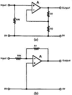
FIG. 3 Feedback systems
There is a limit, in theory, to the performance which can be obtained from such a feedback connected amplifier block, because there will be some failure, however small, in the rejection of the voltage present on both input terminals - the so-called common mode voltage. In the better transistor op amps, the extent of the common mode rejection may be very good, particularly at the lower end of their operating frequency range, but in a simple tube operated differential amplifier, such as the long- tailed pair layout shown in FIG. 1d, the cancellation of common mode signals may not be very good, and distortion due, for example, to the non-linearity of the Ia/Vg characteristics of the two tubes, will not be completely cancelled.
In the circuit layout of FIG. 3b, both the input and the feedback voltages are applied to the inverting input of the amplifier block, in parallel, or shunt, and this mode of operation is known as shunt feedback. The gain of the stage is:
A’ = R1/Rin (9)
…and the input impedance is that due to Rin, because the inverting input will appear to be what is termed a virtual earth, a concept which will be explained later. Since both inputs are connected to the same point there is no common mode error.
The Effect of NFB on Input and Output Impedances
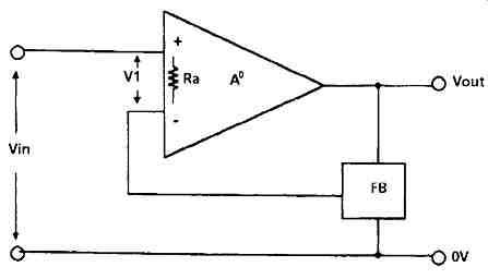
The aspect of the series NFB system can be explored with reference to FIG. 4. In this, the amplifier block has a gain of Ao, Beta is the proportion of the signal which is fed back by the network, FB, V1 is the actual voltage which appears across the input of the gain block, and Ra is the input resistance of the gain block. It is apparent that
Vout = AoV1
But
Vin = Beta Vout + V1
therefore Vin = beta Ao V1+ V1
= V1(Ao + 1)
The actual input resistance (Rin) of the system is:
…which is to say that the input impedance is effectively increased in proportion to the amount of feedback employed.
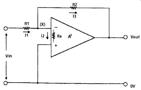
In the case of the shunt feedback layout shown in FIG. 5, if we define the circuit input current as i 1, the amplifier input current as i 2, and the current through the feedback resistor, R2, as i3, then:
i_1 + i_2 + i_3 (11)
and, if the current amplification of the amplifier is Ao, then …
If Vin = i1R1 and Vout =-i3R2, because the gain block is a phase inverting amplifier, then we can determine the circuit gain with feedback (A') which is …
which, if Ao is high enough, will approximate to
A'= - R2/R1
The impedance at point 'X' of an amplifier employing shunt connected NFB (which I have called Ra) can be determined, approximately, by the following argument.
Let us postulate that the gain block is an ideal amplifier in which neither input draws any current, so that i1 = i3. However, because it is an inverting amplifier, the voltage across R2 will be.…
This can be very low indeed if Ao is high enough - much lower in practice than the input impedance (Ra) of any likely amplifier block- so that neglecting the amplifier input current, i2, will not significantly affect the calculated value for Rin. The very low input impedance at the inverting input of any amplifier using shunt feedback has given rise to the term virtual earth to describe its characteristics, and allows the circuit arrangement shown in FIG. 6 to be used as a summing amplifier or signal mixer with very little interaction between the various inputs.
To summaries: the series feedback system offers a very high input impedance, which will increase as the open loop gain of the system is increased. By contrast with this, the shunt feedback layout has a very low input impedance, which will decrease as the open loop gain of the amplifier is increased. In normal shunt FB voltage amplifier circuits, there will be an input resistor, such as R1 in FIG. 5, and this will be effectively the input resistance of the circuit.
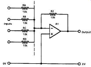
FIG. 6 Virtual earth mixer system
A further important difference between shunt and series connected NFB is that if the feedback limb, between output and inverting input, has zero impedance then, in a shunt feedback system, the gain of the stage will be zero, whereas, in a series feedback system, the gain will be unity. This difference is important in those circuit layouts, considered below, in which the feedback network contains capacitors, whose impedance will decrease, and will ultimately tend to zero as the signal frequency is increased.
 FIG. 7 Arrangement to allow calculation of output impedance
Influence of NFB on Output Impedance
In both shunt and series connected NFB circuits the application of NFB will lower the output impedance of the gain block, as measured at the point from which the NFB is taken. The magnitude of this effect can be calculated by considering the case of an amplifying block with a gain A ~ and an effective output resistance, without feedback, of R o, and has a feedback signal returned to its inverting input via the network, FB, which has an attenuation of Beta.
If a signal voltage, V, is applied to its output, this will produce a voltage Beta V at the inverting input of the amplifier, and this will, in turn, generate a voltage of -Ao Beta V at point 'X'. The voltage across R0 (V0) is given by
V0 = V- Vout ={V-(-Ao – Beta V)}
…and the current through R0 (i0) will be i 0 : V0/R o : V(1 + A~ so the output impedance with feedback, R" 0, which is V/i 0, will be…
…and this effect of lowering the output impedance is the same for both feedback systems.
Effect of NFB on the Harmonic Components of the Signal
A frequently overlooked consideration, in the application of NFB to improve the linearity of non-linear amplifier circuits, is that, in small amounts, NFB can both worsen the total harmonic distortion and modify the distribution of the harmonic components within the distorted signal. The reason for this is simple - that if, for example, an amplifier block introduces second and third harmonic distortion, these harmonics will be present in the feedback signal to the amplifier, and will then be distorted further by the amplifier to produce new fourth, sixth and ninth harmonic components, not present in the original distorted output. So, while the second and third harmonic components present in the feedback will tend, following amplification, to cancel the original distortion components, the higher order distortions will look like a new input signal, which will pass through the system, to be amplified and distorted in their turn.
A practical example of this problem was shown graphically by P. J. Baxandall (Wireless World, December 1978, pp. 53-56), whose results are reproduced in the graph shown as FIG. 8. These figures were determined by measurement on a simple FET amplifier stage, for various levels of applied NFB. For a system using more than 15dB of NFB, the reduction in distortion is as would have been predicted from the simple mathematical model, but for small amounts of NFB, up to, say, 10dB (equivalent to a reduction in gain of 3.3), the distortion could actually worsen due to the increase in the magnitude of higher order components. This problem is more likely to arise in tube operated than in transistor based amplifier systems, partly because it is difficult to get high stage gains from single stage tube circuits, and partly because of the difficulty in applying NFB around multiple stage amplifiers - especially those which employ transformer coupling.
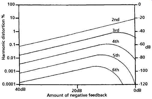
FIG. 8 Effect of NFB on harmonic distortion (Amount of negative feedback)
Practical Tube NFB Systems
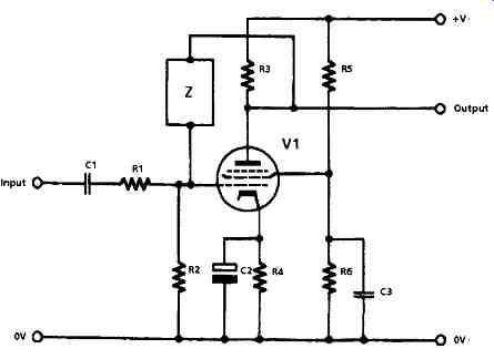
Negative feedback circuit layouts are widely used as frequency response shaping systems, using resistors and capacitors in networks chosen for their impedance vs. frequency characteristics. Such a feedback path, whose input is derived from the anode, can be returned either to the tube grid or to its cathode. By far the most popular arrangement for this type of system is that shown schematically in FIG. 9. In this type of layout a single tube, usually a pentode, is operated under conditions chosen to give a high stage gain, and with shunt connected NFB taken through some frequency dependent network, (Z) from the anode to the tube control grid.
This arrangement would give an approximate stage gain of Z/R1. In early tube preamplifier circuitry both the components forming the feedback network Z and the input network, R1,C1, would be controlled by a multi-position wafer switch to allow a range of different gain/frequency options to be selected to suit radio, or gramophone pick-up, or tape recorder, or microphone inputs.
Although the alternative series NFB connection is possible, this usually means that the feedback signal must be introduced into the cathode of the amplifier tube, which is a very low impedance point, and this presents problems.
A very successful series feedback circuit arrangement, nicknamed the ring of three for obvious reasons, and much favored in physics labs for use as a high gain, linear, wide bandwidth gain module is shown in outline form in FIG. 10. With suitable components this could give a gain of up to several hundred, with very little waveform distortion and with gain/bandwidths flat from, say, 20Hz up to 20MHz or more. The approximate gain of this circuit, which will be constant over a wide frequency band, will be (R7 + R8)/R8.
 FIG. 10 The 'ring of three' feedback circuit
The Baxandall Negative Feedback Tone Control System
Contemporary fashion decrees that the user of Hi-Fi equipment should not attempt to modify the frequency response of his or her equipment to increase or diminish the relative loudness of any part of the audio frequency spectrum with respect to the remainder, and that, instead, the best available fiat frequency response equipment should be purchased, and the tonal rendering given by this should then be left alone.
However, in more practical, and perhaps more realistic, times it was accepted that imperfections could indeed exist, and most of the better audio systems provided some form of 'tone control' to allow the user to compensate for any tonal shortcomings in the bass or treble output of his or her audio equipment.
Of all the circuits suggested for this purpose, by far the most popular -- and adopted by audio designers on a world-wide basis -- was the method proposed by P.J. Baxandall (Wireless World, October 1952, pp. 402-405) of which I have shown the basic layout in FIG. 11. I regret that, among the purists, even this excellent circuit is thought likely to impair the quality of the final sound - even when the controls are adjusted so that the circuit gives a fiat frequency response - and component arrangements are favored in which any desired adjustment to the frequency response is made only by the use of passive components (such as resistors or capacitors) in the belief that these cannot introduce any unwanted worsening of the sound quality.
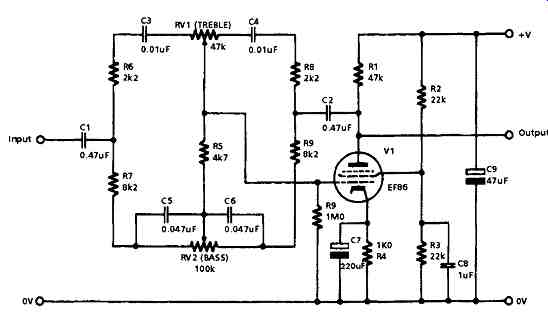
FIG. 11 Baxandall NFB Tone Control
Unfortunately, this argument is fallacious in that, for any passive tone control to work, it must introduce an overall attenuation in its fiat frequency response mode which is at least equal to the desired boost in gain at the desired frequency (treble or bass) relative to its gain in the mid-range. So, in order for the overall gain of the system, including the control circuit, to be the same as it had been before the circuit was inserted, an additional (distortion introducing) gain stage must now be used to make up for the loss of gain due to the passive circuitry. Unfortunately, this amplifier stage is likely to introduce more distortion than that of the equivalent stage within the feedback system, because any distortion introduced by this will be reduced by the internal NFB within the circuit. This argument applies equally to such circuit as filters or fixed frequency response adjustment networks (i.e. for gramophone PU output equalization) as it does to tone controls.
To understand the operation of the Baxandall circuit it is convenient to postulate that the two tone controls are set at their mid positions (in Baxandall's original circuit, the potentiometer RV2 was center-tapped, and this tap was connected to the 0V line, but in normal practice, this refinement is omitted, since the circuit works quite well without it). In this case, the input limb of the circuit (to V1 grid, which acts as a virtual earth because the circuit employs shunt connected NFB) is R6,C3 and half RV1 in parallel with R7,C5 and half RV2. The feedback limb is, similarly, R8,C4 and half RV 1 in parallel with R9,C8 and half RV2. Clearly, at all audio frequencies, these two limbs are equal in impedance and the circuit therefore has a gain of unity.
If the slider of RV1 is moved to the left, then, at (treble) frequencies at which C3 and C4 have a low impedance, the impedance of the left hand (input) limb of this network will be less than that of the fight hand (feedback) one, and the circuit gain will be increased up to a limit value of:
Treble gain (or attenuation) - (2200 + 47,000)/2200 = 22.3
…which is just over 26dB. Conversely, if the slider of RV1 is moved to the right, the gain at treble frequencies will be decreased to an ultimate attenuation of-26dB.
A similar argument can be used to determine the limit increase in gain, or the limit value of attenuation at those very low audio frequencies at which the impedance of C5 and C6 is much higher than the resistance of RV2. In this case, the bass gain will be Bass gain (or attenuation) = 108 200/8200 = 13.2 which is just over 22dB. Intermediate settings of RV1 and RV2 will provide intermediate levels of lift and cut of either treble or bass, and these adjustments can be made simultaneously, and with very little cross influence. Also, the amplifier tube will have an open loop gain of about 50, and this will reduce the closed loop distortion (at mid-frequency range) to about 0.01% at 6V rms output.
By comparison with this, a similar gain stage following a passive tone control layout, with NFB used to adjust its gain to, say, 25, will have a distortion (at mid-frequency range), of about 0.2% at 6V rms output. The drawback in both cases is that any treble boost, even in a distortion-free circuit, will enhance the amount of harmonics of the signal as it increases the treble gain, relative to that of the waveform fundamental frequency. On the other hand, treble attenuation will reduce the THD. An analogous and very obvious phenomenon, within the experience of any user of vinyl gramophone record discs, is that any use of bass boost will exaggerate the audible, low-frequency rumble noise caused by imperfections in the turntable beatings.
Frequency Response Equalization
In the early years of the manufacture of 78rpm emery-loaded shellac gramophone record discs a variety of modifications were made to the frequency response of the recorded signal in the hope that the inverse frequency response, used on replay to recover a fiat frequency output from the recorded signal, would lessen the surface noise of the disc, and increase the practicable recording levels. By the time the vinyl (LP) gramophone record was introduced, in 1951, universal agreement had been obtained on the type of record and replay characteristics. The agreed standard, for both 45rpm and 33rpm discs, is shown in FIG. 12, and is generally known as the RIAA response curve because it was proposed by a consultative committee from the Radio Industries Association of America.
A typical gramophone record replay circuit, of which the characteristics have been tailored to give an RIAA type replay frequency response, is shown in FIG. 13. This circuit gives a stage gain of 10 at 1 kHz, and since the input signal is likely to be small, a cascode layout is chosen to give the lowest noise practicable from a shunt feedback circuit.
As seen from FIG. 12 it is required to generate a gain/frequency response curve which rises, below l kHz, at which frequency the relative gain is 0dB (unity) to +3dB at 500.5Hz, and +17dB at 50.05Hz. Above 1kHz the relative gain is required to decrease from-3dB at 2121.5Hz to -20dB at 21.2 l kHz. This type of response curve is produced by the two parallel RC groupings shown as R2C2 and R3C3 in the circuit drawing, since the overall gain will be determined by the relative impedance ratios of the two limbs R2C2 and R3C3 relative to R1C1. The method by which the required component values can be calculated is given in the book The Art of Linear Electronics, as is also a rather fuller account (in Section 7) of the use of NFB in audio systems.
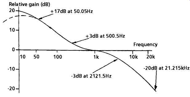
FIG. 12 RIAA equalized frequency response
Filter Circuits Based on NFB
D.T.N. Williamson, in part of his celebrated series of articles describing a very high quality audio amplifier and preamplifier (Wireless World, October/November 1949), described two circuits in which he used a combination of a frequency selective feedback arrangement and a parallel-T notch filter to provide a steep cut high pass rumble filter and an equally steep cut, but switched frequency low pass filter which would serve to reduce the amount of audible high frequency hiss resulting from the emery powder loading of the shellac body of the contemporary 78rpm records.
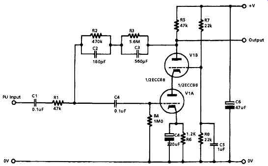
FIG. 13 Phono (RIAA) pick-up input stage
The basic layouts of these two filter types are shown in FIGs 14a and 14b, and the frequency response of the final circuitry incorporating these is shown in FIG. 15. The method of operation of both of these filter circuits is the same: if NFB is applied around a circuit in which there are two RC low pass networks operating at a similar roll-off frequency, the action of the NFB will be to flatten the frequency response up to some turnover frequency determined by the RC networks, beyond which the output will fall at an ultimate rate of-12dB/octave.
In the case of the low pass circuit shown in FIG. 14a, the two RC networks are formed by R4,C1 and R7,C5. By introducing a parallel-T notch filter (R2,R3,C4 and C2,C3,R5) into the signal path, and then taking the NFB point from the output of this, the overall flatness of the frequency response is maintained, but the slope of the HF roll-off beyond the turnover frequency is increased by the notch circuit to about -40dB/octave.
The action of the high pass filter circuit of FIG. 14b is essentially similar, except that only the first of the two CR networks (C1,R10 and C4,R7) is within the feedback loop, and the T network is bridged to reduce the ultimate attenuation rate to about -30dB/octave, which Williamson judged to be sufficient to remove rumble noises due to turntable beating imperfections.
The detailed design of these circuits is given in a reprint of his original articles (Williamson, D.T.N., Wireless World, August 1949-May 1952. Reprinted in 1990 by Audio Amateur Publications, Inc., Peterborough, NH, USA).
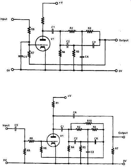
FIG. 14: a Low pass filter; b High pass filter
 FIG. 15 Filter characteristics
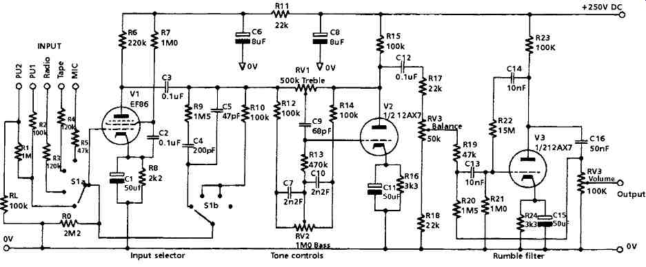
FIG. 16 The Brimar SP55 preamp
An alternative example of tube operated preamplifier design, the Brimar SP55 stereo preamp, is shown in FIG. 16. This dates from the middle 1950s and is quoted in the Brimar Tube and Teletube Manual Volume 9. This is a typical, and well- engineered, example of circuit design at a period when the situation with regard to gramophone record replay facilities had stabilized with the more or less universal adoption of 33 1/3 rpm LPs and 45 rpm EPs in place of the easily broken 78rpm shellac discs. Because hiss on record replay was no longer a problem, steep-cut treble filters of the type Williamson proposed were no longer much needed, and were seldom offered. Also, with the new vinyl discs came an agreed (RIAA standard) replay frequency compensation characteristic and an effective choice between high performance and expensive electromagnetic pick-up cartridges, and inexpensive and popular piezo-electric systems, usually based on a piezo-electric ceramic element.
For both of these cartridge types a standard load of 100k was adopted (contemporary usage would favor a load resistance of 47k) which was supposed to constrain the ceramic cartridge into an electromagnetic style of performance, for which, with both types of input, the frequency response would be corrected by the network R9,C4,C5 in the anode-grid feedback path of V1. For all the other inputs provided, V 1 would act as a fiat frequency response stage whose gain was determined by the input and feedback networks, with the exception of the microphone input where no input stage NFB was employed.
This allowed V1 to have a stage gain of about 200, and gave input sensitivities, for maximum output: Mag. p.u, 8mV, Ceramic p.u, 60mV, Radio/Tape recorder, 100mV and microphone, 2.5mV. The resistance network connected around V2 implements a Baxandall type feedback tone control circuit, for which the quoted performance is: Treble lift/cut, + 13dB at 10kHz, ref. 1 kHz.
Bass lift/cut, + 16dB at 50Hz, ref. 1 kHz.
The final stage provides an input channel balance facility coupled with a permanently connected rumble filter, with a fiat frequency response down to the cut-off point beyond which the gain would fall rapidly, with an ultimate attenuation rate of -18dB/octave. This filter characteristic was generated by NFB through the two feedback loops, C14, R22 and C16,R20,C 13, connected between anode and grid of V3.
A roll-off frequency of 28Hz was adopted in this design since it had by now become generally accepted that there was little below 30Hz which was either part of the musical content of the recording or capable of reproduction by anything but the very best of LS systems.
The design figure for signal output, with tone and balance controls set at mid-position, and the volume control set at its maximum output position, was 500mV, at which the distortion figure would be less than 0.05%. The quoted signal/noise ratio for the disc inputs was better than -55dB, and for the radio and tape inputs, better than -65dB.
Although modern design practice would allow some improvement on these signal/noise figures, it is in this respect that the biggest difference exists between tube and solid state technology, for which a disc signal/noise ratio of, say,-85dB would be normal, and a flat frequency response auxiliary input position (such as provided for a CD replay input) should offer signal/noise ratios of the order of-100dB.
