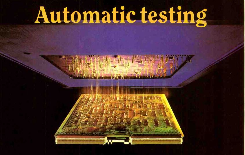
An overview of techniques used in the automatic testing of printed-circuit board assemblies.
by GRAHAM ELLIOTT
Automatic test equipment, a.t.e., is widely used to test electronic components and printed-circuit board assemblies. It comprises a set of test instruments whose functions are controlled by a computer via a test program. A test fixture provides a hardware interface through which access to the unit under test is achieved. The a.t.e. market breaks down into three major groups; PCB testers, component testers and bare board testers. All a.t.e. systems can have a great effect on the commercial viability and attainment of quality and specification for a variety of electronics products.
The accelerating growth of technology means that improved and more complex devices are coming to market faster. Product lifetimes are reduced and the problems of developing and introducing new lines amplified. Customers now familiar with high technology products demand a very high level of reliability. The general shortage of skilled electronics engineers makes the application of manual test stages impractical and existing stages of automation have grown to provide the solution. Efficiency, productivity and quality are all improved while costs are reduced. The use of automated systems in design, manufacture and test has increased dramatically over the last few years, and a.t.e., in particular, provides important information relative to scheduling, costs and product quality.
WHY TEST AT ALL?
Testing electronic devices and assemblies is an expensive process and one might well ask why test at all? If designs were error-free, all components purchased functioned to specification, all sub-assemblies were correctly connected and no calibration or adjustments were needed, the product could go directly to the customer. Unfortunately it is not a perfect world and should a manufacturer choose to omit the test stage it would soon go out of business; field service costs would be astronomical and a reputation for poor quality and reliability would quickly put off prospective customers. Testing is an essential part of the manufacturing process, providing a high degree of confidence but, because of the costs involved, must be performed only at key points in the process to be economical.
It is possible for testing to take place at every stage in the production line shown in Fig.1. But to do so would waste resources and result in less than optimum performance. Usually a fault coverage of around 95% can be achieved at a reasonable cost, the remaining 5% being uneconomical for most companies to achieve and requiring a disproportionate investment in additional equipment. The a.t.e. systems described below may be implemented at any stage, each having been designed to match the requirements of a particular point in the production process.
Component testers. These range from small bench-top bridges to large parametric testers. The latter perform full parametric tests on integrated circuits prior to their insertion into printed circuit boards. Costs range from a few thousand pounds for the smaller systems to several hundred thousand pounds for the parametric testers. The installation of parametric testers is not usual for most applications.
Bare-board testers. Blank PCBs may be tested on bare-board testers prior to their population with components, each track checked for breaks and spurious short circuits. Test speeds and board throughputs are high, making their application popular where expensive or very high volumes of printed-circuit boards are used. Prices begin at approximately twenty-five thousand pounds and fixturing costs (fixtures providing a hardware interface between tester and a PCB under test) are minimal. Bare-board testers are usually used prior to later testing on in-circuit or functional a.t.e..
Manufacturing-defect analyzers. M.d.a’s detect manufacturing process faults by testing for track continuity, spurious short circuits, component presence, correct value and orientation, without applying power to the printed circuit board or assembly. They are often used with other testers, pre-screening PCBs prior to in-circuit or functional testing. Costs for m.d.a’s commence at approximately thirty-five thousand pounds.

---------- Bench-top automatic test equipment
In-circuit testers. If a printed-circuit board is correctly manufactured and each component correctly fitted and operational, then the PCB will function correctly. That is the principle on which in-circuit testers are based. Track continuity tests and checks for spurious short circuits are performed, although not as quickly as on the bare board tester. Passive component measurements establish presence, value and orientation of discrete components. Controlled powering up of the board prevents component failures occurring at this stage, which is followed by active analog and digital tests. In-circuit testers are available in the range £ (x1.34 for $)25,000 to £ (x1.34 for $)200.000.
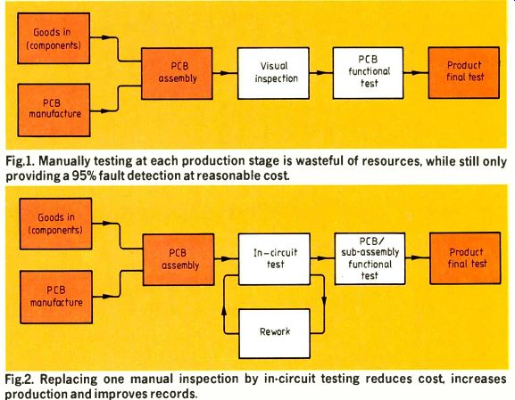
Fig.1. Manually testing at each production stage is wasteful of resources,
while still only providing a 95%fault detection at reasonable cost. Fig.2.
Replacing one manual inspection by in-circuit testing reduces cost, increases
production and improves records.
Functional testers. A different test strategy is used by functional testers, that of testing the PCB as a single functioning unit. This is done by injecting a series of test patterns into the p.c.b's inputs and monitoring for expected patterns at the outputs. When errors occur, diagnostic algorithms, generated by simulator software, identify the failing component. This method is particularly effective for locating digital device errors occurring at high speed, functional testers operating at speeds of up to 30MHz, as opposed to the 1MHz digital test rate generally available from in-circuit testers.
Prices for functional test systems range between £ (x1.34 for $)150,000 and £ (x1.34 for $) 250,000 (bench-top testers start at around £ (x1.34 for $)50,000).
Traditional a.t.e. tends to be rather large and expensive, but smaller and cheaper bench-top systems are also available, as indicated above. The performance of these systems, in terms of test speed, PCB throughput and test-point capacity (the maximum number of circuit nodes with which the system can make contact) is generally lower than the larger systems. But bench-top systems are attractive, since they provide an entry path into automatic testing for small organizations unable to afford the traditional types. Larger companies may choose to purchase several system, providing virtual immunity to failure and allowing a more flexible test strategy.
The option therefore exists to test at every stage, and the best place or places to test will depend upon the requirements of the particular installation. Identifying the optimum point at which to site test equipment is achieved by analyzing the types and proportions of faults occurring. A typical production line may suffer the following failures:
30% short circuit tracks
25% faulty components
12% unsoldered or dry joints
9% wrongly fitted components
8% wrong components
2% broken components
2% open circuit tracks
To determine the optimum position in the production line to place test equipment, one must first consider how and where the faults occur. Short circuits and soldering problems are likely to occur at the soldering stage, while most wrongly inserted, wrong and broken components are introduced at the component insertion stage prior to soldering. Broken components and open circuit tracks can be introduced at any point, but are more likely at the earlier stages, or during rework. Any areas of manual assembly are often a weak link in the chain and are susceptible to any of these types of error.
One must now assess the most suitable tester test option.
Continuity testing will only find the track-related faults introduced prior to board assembly, a small proportion of those identified. Component testers find a similarly small proportion of PCB faults. A manufacturing-defect analyzer will find most of the faults in the list, but not those requiring active tests (a possible 25%). The functional tester positioned at the end of the assembly line is better placed, but is not best used to detect track and analog failures, being very effective at locating digital faults.
This is also the most expensive system to buy and operate.
In-circuit testing provides the best solution in this case, being capable of detecting all of the fault types in the analysis. All PCB failures are detected during a single test of the board, enabling a high throughput to be maintained, and fault reporting to component level simplifies rework.
The in-circuit tester. The production process diagram of Fig.1 now becomes that shown in Fig.2. If the in-circuit tester replaces a manual test stage, several advantages immediately become apparent; skill level at the test stage and cost per PCB are reduced, documentation is improved and production capacity is increased.
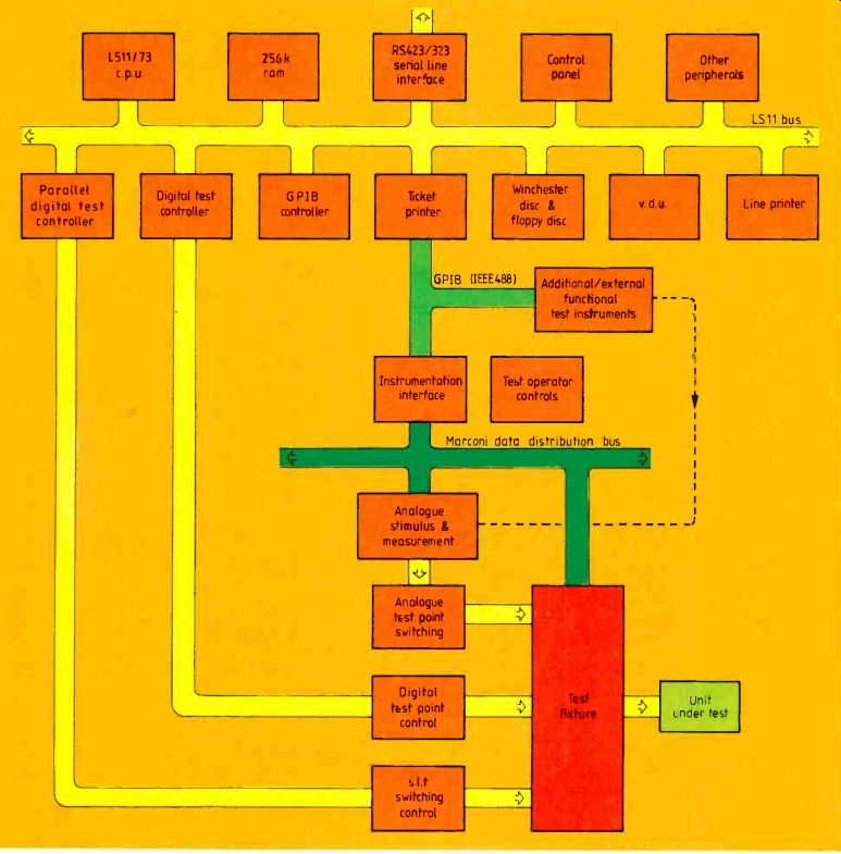
Fig.3. System architecture of an in-circuit tester.
Producing the test program and fixture. A block diagram of system architecture is shown in Fig.3. The central computer controls the operation of the analog and digital test electronics. In some applications one may wish to connect external GPIB controlled measuring instruments to the PCB under test, and this may be done through the in-circuit testers' own hardware interface. System software will control the operation of these instruments via a GPIB port.
The operation of the hardware is invisible to the program, the high-level programming language automatically configuring the a.t.e.'s measuring instruments to perform the necessary measurements. There are three basic steps in the generation of a working test program and fixture.
The first step is to allocate test points (which connect the a.t.e. hardware to the PCB) to a circuit diagram of the board to be tested. This allocation will use the analog and digital test points available on the test system, and is very straightforward. Once complete, it is transferred to a 1:1 artwork of the PCB The artwork is used by the fixture manufacturer to ensure accuracy: in-circuit testers use a hardware interface known as the 'bed of nails' fixture to provide easy an accurate connection to the board under test.
Figure 4 and the accompanying photograph show a section through a bed of nails fixture and a picture of it in use. The fixture relies on accurately positioned spring probes (or test points) and the marked up artwork gives these positions. Wired back to an interface block which connects to the tester, they make contact with every electrical node (i.e. component interconnection) on the board.
This requires very accurate positioning and registration, target areas for the probes typically being component leadouts or special dedicated pads. Location pins on the fixture are made and positioned to match artwork-referenced fixing holes in the p.c.b, the holes being chosen to ensure that the board is correctly oriented. Operation of the fixture is quite simple: the PCB is positioned on the fixture's carriage plate and the 'operate' button pressed. A vacuum source, external to the test system but piped through it, evacuates the air between the carriage and bed plates, sucking the board onto the probes.
The second activity, occurring in parallel with the manufacture of the fixture, is the generation of the test program. Software provided on the a.t.e. prompts for parts-list information, such as component identifier, nominal value, tolerance or device type and the assigned test point numbers for each component. Active tests for digital devices are stored in a disc-resident 'library'. Special software locates the active test for the specified device and converts it to the high level program language, appending the relevant test point information as part of this process. When all parts list information and the library-based tests have been added to the program, a second programming stage takes place. The program is analyzed and partially debugged by a special software package which searches for device con figurations which affect the accuracy of measurements performed by the a.t.e.
'Guard' points and other special test routines, for example bus tristate and open-collector test, are automatically added and the circuit checked for potentially dangerous testing and circuit configurations.
The final activity is to prove the test fixture and program together on the a.t.e. This final program debugging resolves all remaining test problems and the PCB can now be production tested on the a.t.e.
Order of test execution. In-circuit test execution is carried out in the following order:
track tests for continuity and spurious short circuits, tests for the presence of wire links, measurements of discrete components, a controlled powering up of the PCB and active analog and digital tests. All faults are usually located on a single run of the test program, although the program run will be aborted if the track tests fail. This avoids the possibility of damaging the PCB by applying power to it while there are track shorts on it. The test program is also aborted if an error occurs while performing the initial PCB power up prior to the active analog and digital tests.
Analog test pin electronics. The analog test-point switching system connects specified test points to the measurement hard ware and is fundamental to accurate and flexible analog measurement. It must be capable of performing an efficient scan for random short circuits between two or more points, provide high insulation between test points and system ground, enabling resistances of at least 10 milliohms to be measured without significant error and allowing leakage measurements to be performed. For capacitors in the order of 10 picofarads to be measured, inter-test point capacitance must be limited.
A number of design features allow these requirements to be met. Mechanical switching elements meet the isolation and series impedance requirements. A three-tier switching 'tree' reduces the selection time for specified test points and reduces stray capacitance in the switching system. A technique to solve the problem of single-pole switch losses is to employ p-n-p transistor switch-control stages. This avoids driving the coils direct from high-power, open-collector integrated circuits and all switches have their coils at zero voltage, minimizing coil-to-switch leakage. 'Break-before-make' operations protect the system from possible damage from stored charge in the board under test. The reed relays used are especially designed to minimize the effect of thermal e.m.f.
Analog measurement techniques. The analog measurement system is shown diagrammatically in Fig.5. It features two reference power supplies, a programmable resistor, a 12 bit analog-to-digital converter and a measurement zero-volt line. These may be connected to any analog test point via the four-pole switching matrix. The poles (or wires) of the matrix are designated A, B, CO, and CI .
An a-to-d converter is used in place of a digital voltmeter for greater speed. The system also features additional fast, floating reference power supplies to provide power to the PCB under test and stimulus for digital device drivers.
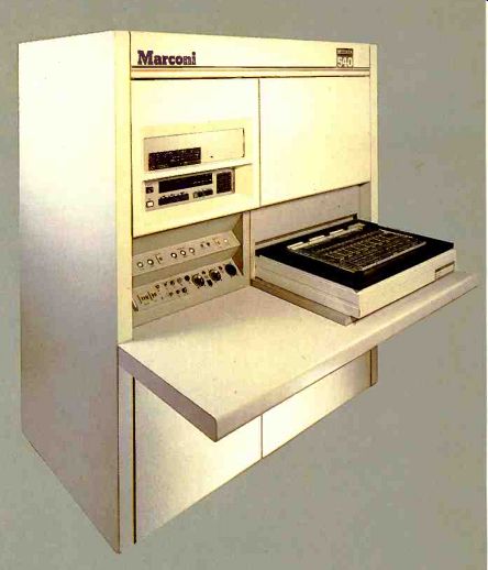
--------------Marconi MIDATA 540 in-circuit tester.
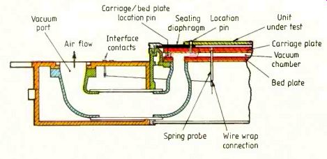
---------Fig. 4. Section Through a bed-of-nails test fixture.
Under normal operating conditions, the system configuration for all standard measurements is arranged automatically by the high-level test language. However, experienced programmers have the option of full control of all parameters through the test program, enabling special non-standard tests to be performed if required.
Resistance measurement. A simple example of how tests are modified to cope with certain measurement conditions is the resistance test. The theoretical measurement circuit is shown in Fig.6. Rx is a resistor in the range 40051 to 20MSZ. The high gain and high input impedance of the operational amplifier results in points X and Y being equipotential. Provided that system switch, lead and contact resistance are negligible compared with R,, the gain equation of the operational amplifier is
\Tout-Vref Rref R.
or RXor1 Vout
This configuration is often sufficient to provide a reliable test for a resistor, but the component configuration shown in Fig.7 is more, often encountered. When testing R5 there is a low-impedance path through resistors R4, R9 and R10. Referring to Fig.8, the combined shunt resistance of these components will significantly effect the measured value of R5.
Test point 5 is selected as a 'guard' point and connected to pole C. R4 shunts the voltage source, so provided it does not pass too much current it will not effect the voltage at Z. Since X and Y are equipotential, the series combination of R9 and R10 does not pass any current and the original gain equation remains true.
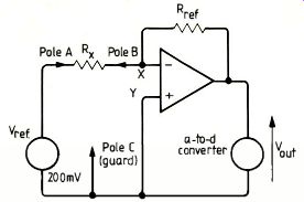
Fig.6. Resistance (RX) measurement in basic form.
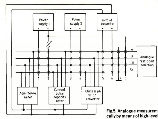
Fig. 5. Analog measurement system, which is normally configured automatically
by means of high-level test language.
Fig. 7. More usual resistance-measurement circuit, in which shunt resistance
affects measurement.
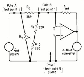
Fig. 8. Circuit arrangement in which shunt resistors of Fig.7. are either
shunting the source or across the equipotential points and do not affect
reading.
The system will also perform a special low-value resistance test (using Kelvin techniques) and an a.c. resistance measurement where a resistor is shunted by an inductor.
Other measurements include those on capacitors, inductors, leakage, diodes and transistors. Space does not permit the discussion of examples of these types of measurement.
Digital test execution. A prime requirement of all automatic test equipment is the location of faults to component level. Most in-circuit test systems meet this requirement when testing digital devices by using a test method known as node forcing. Digital pin drivers force logic levels at the device's inputs or control pins and override the normal quiescent state of the node due to preceding stages. The resulting logic states at the device outputs are monitored to establish the correct functioning of the device without needing to propagate logic states through complex digital circuitry.
Much discussion has taken place as to the long-term effect of this method on other components on the PCB Research has shown that it is the output stages connected to a force node which are stressed by the currents used in node forcing and that junction temperature rise within the device is the main hazard. Tests have shown that for node forcing to cause a t.t.l. device to reach a junction temperature of 70°C under normal ambient conditions of 25°C, a forcing period of at least 30ms is required. The tester therefore applies a hardware timeout of 400µs on all node forcing stimuli, ensuring total device safety. The biggest advantage of node forcing is that it is easy and quick to program and provides a high test speed.
When the test program is run, each test routine is loaded from computer memory into a local high-speed ram under system software control. Up to 2048 test instructions may be stored in this ram at any time and a high test speed is achieved by making the speed of test execution independent of the LSI11 computer. The ram outputs at 1MHz with the test instructions being executed one per microsecond: tests for s.s.i. and m.s.i. devices typically require only a few test steps, so the hardware timeout is not exceeded. A truth-table system drives input and control pins and monitors for outputs as expected from the devices' truth table.
Failure of any part of the test results in device and PCB failure. More complex digital devices are tested using the same basic method, although the tests do not follow the same truth-table approach. This serial test method may be supplemented with a parallel test method, setting up a series of pin states simultaneously and achieving a much faster test rate.
FUNCTIONAL TESTING
The main advantages of in-circuit testing are; inherent fault diagnosis to component level, low programming cost and skill requirements and short programming times.
The disadvantages of this method are relatively high recurring fixture costs and the inability to detect faults which only become apparent at or around the p.c.b's normal operating speed, for example timing problems. These are especially important in some applications, for example military products, where these faults must be found at the board test stage, rather than final test. For example, the electronic systems in a rocket only have one chance.
This latter type of fault is located by another a.t.e., the functional tester. The function test program injects a pattern of stimuli into the inputs of the PCB and monitors for expected results on the outputs. If the PCB fails, diagnostic software, using a technique known as reverse trace, guides the operator back through the PCB network from the output, prompting the operator to probe specific nodes with hand held probe, wired back to the a.t.e., until the failing component is located.
Generating the test program and software is quite a complex task and is usually carried out by a software package known as a simulator. One widely used simulator will run on a variety of functional a.t.e. systems or on a mainframe computer. To generate the necessary software for functional testing, the programmer must take the following steps.
A database or image file, containing de tails of all devices on the PCB and their interconnections, must be written. To do this, the programmer simply specifies each component connection (e.g. ICI pin 1) and the track or signal name to which it is connected. When processed by the simulator the signal names reference particular component pins on the same node to one another, producing a network description of the PCB.
The database is now run through the first part of the simulator where mathematical models of each device fitted are located and combined, using the network description of the p.c.b, to produce a mathematical model of the whole board. This is in Boolean algebraic form and it is using this model that the sequence of input stimuli and expected output results are determined.
The simulator now produces series of input stimuli and applies them to the mathematical model of the PCB When this pro cess is complete the following files are produced: the test program; a file indicating the percentage of possible faults that will be detected by the test program; a list of untested nodes; wiring lists for fixture manufacture; the diagnostic files to be invoked should a p.c.b test fail.
An important requirement of functional testing is good node visibility: i.e. should any single node fail that failure must be flushed through to and be visible at the PCB output. If good node visibility is not achievable a partial bed of nails fixture may be required to supplement the standard edge connector `fixturing' and provide the necessary node visibility.
When creating and debugging files the programmer has some additional software tools available: a database creator aids the programmer at the PCB description-generation stage: an emulator, part of the simulator, creates mathematical models for complex digital devices; and a logic analyzer shows the logic state of any node at any stage during the test and is particularly useful when creating and debugging new mathematical device models.
Functional testing has several advantages over in-circuit testing. Fixturing costs are low, and the PCB is tested at or near its actual operating speed (up to 30MHz on some functional testers). Further, timing problems in digital circuits can be detected and their source identified. PCBs which have been conformal coated can be tested, since the edge connectors are clear and the diagnostic probe is able to pierce the coating. In-circuit testers must test PCBs prior to the application of the coating. Additionally, surface mounted devices do not pose any special problems, whereas true in-circuit testing sometimes requires the use of special (and expensive) fixturing.
However, in-circuit testers have advantages over functional testers, in that functional hardware is much more expensive than in-circuit testers, and in-circuit testing requires a much lower skill level than functional testing, typically taking one fifth of the time to write, for the same PCB. A functional tester can only find one fault on each test run and these often take some time to locate using the reverse trace method.
In-circuit testers find all faults on a single pass in a much shorter time.
PRODUCTION LINE USING ATE
Once installed in the production line, a.t.e. provides a number of benefits. Throughput is increased: for example an in-circuit test time around 10 seconds would not be un usual for a PCB comprising 60 discrete and 60 digital components (including track testing). Quality is improved as the level of inspection or test does not vary. For example, manual visual inspection of a p.c.b, in addition to being slower, is dependent on the degree of concentration of the inspector, which varies during the day, and also throughout the week.
When the a.t.e. is fully utilized in testing p.c.b’s, it may become difficult to find sufficient free time to write new test programs.
Off-line programming on a multi-user work station reduces the time required on the a.t.e. to that needed for fixture and program debug.
Efficiency may also be improved in the rework area. When faults are found by an in-circuit a.t.e. they are printed out on a paper ticket. This contains details of the component identity and its failing value if analog, or device type if digital. But as component packing densities increase, the PCB legend is usually omitted, making component location difficult. If a track short is found, the a.t.e. can only report the test point numbers between which the short circuit occurred. On a large double-sided or multi-layer board it can take the repair technician many minutes to simple locate the fault. Computer aided repair (car) provides a solution: the paper ticket is replaced by a software fault file, sent to a multi-user workstation by a a.t.e. via a wire link. When the board goes to the rework area for repair, the technician enters its serial number, possibly using a bar-code reader, and the fault file belonging to that PCB is read.
Faults located on the test run are displayed on a full color graphics display which shows the location of all components or tracks on that board type. Fault location time is greatly reduced and productivity in the repair area increased.
Information about the types and numbers of faults from both the a.t.e. and car can be put together by process-management soft ware to give a 'real-time', up-to-the-minute picture of production. The most frequently occurring failures, identified either by component identity, or failure type, for a particular PCB production run is displayed. Analog failures may also be checked for the spread of failures around the nominal value.
Using this software, earlier process errors, e.g. a wrongly set flow solder bath, may be identified and the line stopped until they have been corrected.
THE FUTURE
A.t.e. capabilities have improved, some of today's low-cost bench-top a.t.e’s having a superior performance and specification to the larger testers available a decade ago.
Many manufacturers are attempting to combine the capabilities of in-circuit and functional testers into a single test system. These combinational testers will overcome the limitations of the two system types, although no company has yet succeeded in bringing a true combination tester to market at a realistic price.
But perhaps the most important development in the industry is that of data sharing.
Real-time fault analysis is one example of how data gathered at the a.t.e. stage can be put to good use elsewhere. Another example is taking the PCB design information avail able in a computer-aided design system files and automatically producing an a.t.e. test program. Such a system is already available and also generates car and fixture design files, greatly reducing development costs and times.
The future of the industry lies in integration. Automation reduces manufacturing costs, but it is integration which reduces the applications costs associated with the introduction of new products (e.g. test programs, manufacturing information). When these are overcome the 'factory of the future', much heralded within the industry, will be much nearer. A.t.e. is playing a key role.
-- Graham Elliott is with Marconi Instruments, St. Albans.
------------
Also see: Electrometer amplifiers for sub-pico-amp currents
Television standards conversion
==========
(adapted from: Wireless World , Jan. 1987)