Switched-range and logarithmic amplifiers for currents down to 20 femto-amps.
by D.F. CAUDREY
Electrometer amplifiers are widely used in the nuclear industry for amplification and measurement of direct currents from ionization chambers used, for example, in reactor control and safety instrumentation. In these applications they process currents ranging from femto-amps to nanoamps (10^-15 A to 10^-9 A).
This article presents the basic design principles for a switched-range linear amplifier and an examination of those concerned with its single-range logarithmic counter part. To quantify the design parameters, it is assumed that either type is to measure currents over the four and a half decades from 20 femto-amps to 0.6 nanoamps; in the linear case, by ten switched ranges -- 20fA f.s.d. multiplied by 1,3,10, 30 and so on to 0.6nA f.s.d.
DESIGN PRINCIPLES
Figure 1 shows a block diagram of a direct-coupled measuring amplifier. The current flowing through the milliammeter, Iot, is essentially equal to
I_in Rf/Rm
provided that no current is diverted to or fed from the amplifier input terminal and the loop gain ARm//(Rm+Rt) is much greater than unity.
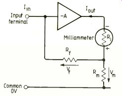
Fig.1. D.c. amplifier block diagram, in which l,n is the input current;
RF the input resistor; R,,, a range-multiplier resistor; R, the internal
resistance of the meter; and V,,, the range voltage. The meter can be
replaced by a resistor terminating the input to a d.p.m., simpligyinh
range switching.
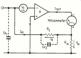
Fig. 2. Voltage generator Vt represents temperature and other sources
of drive.
The amplifier must, therefore, have very high input resistance, its gain must be large and Rm must not be much less than R1. From expression (1) it can be seen that Iot is directly proportional to I; and is equal to Iin multiplied by the factor -R1/Rm, the current gain of the amplifier. It can also be seen from (1) that lout is independent of the resistance of the milliammeter and within reason any milliammeter may be used to indicate the magnitude of the input current.
The range voltage Vm is given by I_out Rm and inserting this into (1) gives Vm=-Iin Rf.
Therefore Vm is equal to, but opposite in polarity to VI, the voltage drop across R1 due to I. Of course, V1 and Vm differ by the voltage needed to drive the amplifier, which is V1/loop gain, but if loop gain is very high the drive voltage will be virtually zero. As will emerge later, this virtual-earth input is an essential requirement for current-measuring electrometers.
Choice of range voltage. Consider the most sensitive range of 20fA f.s.d. and assume that this is to be displayed on a 1mA f.s.d. meter.
From (1) the magnitude
Therefore or lout Rf I_in Rm Rf 10-314-5x10¹⁰ Rm 2X10 Rf=5x10¹⁰Rm (3) (2)
Thus it would appear that any combination of resistors having this relationship could be used to achieve the desired result. However, the amplifier shortcomings must be taken into account. All directly-coupled amplifiers are subject to drift, both as a random function of time or as a result of temperature change. Fortunately, time-dependent drift is small in solid-state amplifiers, but the effects of temperature have considerable bearing on the choice of Vm. In common with most solid-state, directly-coupled amplifiers, the electrometer amplifier is a balanced, differential type having one input terminal driven by the input signal and the other held at a reference potential. This, of course, minimizes the direct effects of temperature and supply voltage changes by rendering them common-mode, and the degree of temperature independence achieved depends on the matching of temperature coefficients in the balanced input stage. In all practical electrometer circuits, there will be appreciable temperature dependence.
The temperature dependence of operational amplifiers is usually expressed in terms of the equivalent difference voltage between the input terminals and, for modern monolithic integrated circuits, figures of 1 to 5µV/°C are commonly specified. Unfortunately, due to the need for very high input resistance, it is essential to employ mosfet transistors in the input stage of electrometer amplifiers; devices which can normally be matched to better than 100 uV/°C in monolithic pairs. Consequently, the virtual-earth driving point can drift by up to 2mV for 20°C temperature excursions. This effect, together with other sources of drift, can be represented by an additional voltage generator Vt, as shown in Fig.2.
As V1 is within the feedback loop, it must be small in comparison with Vm (-V1) if the dominant temperature-dependent drift is not to be a nuisance. However, the choice of Vm is constrained by the maximum permissible value for the feedback resistor R1 and its relationship to Rm defined in expression (3).
High-value resistors are available in values up to 100 T-omega (10^14 omega) but about 3 T-omega is the maximum value which gives accept-able selection tolerance (1%) and stability in respect of temperature and voltage coefficients and ageing. This constraint defines Vm as 60mV for the 20fA f.s.d. range. For the higher ranges of input current, it is possible to reduce R1 or to increase Rm and concomitantly Vm. Of these options, the former gives the benefit of reduced response time, as is discussed later, and the latter is less costly, because fewer expensive, high-value resistors are required to accommodate the projected ten ranges of current measurement.
The latter option also simplifies the range switch at the input to the amplifier, with a consequent reduction in static-charge over loads during range selection. In fact, it is possible to employ only two values for R1 (3T omega and 10G ohm) in conjunction with seven values of Rm to cover the assumed range of current measurement 20fA to 0.6nA.
Response time. Also shown in Fig.2 are two stray capacitances Cs1 and Cs2, which can influence the response time of the electro meter amplifier. Cs1 represents the input capacitance made up mainly by the capacitance of the signal source-ionization chamber etc.- and the gate capacitance of the input mosfet. The magnitude of C51 might be as much as 100pF and, by virtue of its position, it must be charged by the input current before the electrometer can achieve a correct indication. Remembering that Vm for the 20fA range is 60mV, it is worthwhile to examine the time required for the input current to charge 100pF to 60mV
t=CV/1=100 x 10^-12x 60x10^-3 seconds.
/ 2 x 10^-14
Therefore, without virtual-earth operation, f.s.d. would be reached after five minutes.
However, for the most critical 20fA range, the loop gain ARm/(Rm+Ri) for the projected design is likely to exceed 40,000 if a typical operational amplifier is included in the loop, and thus Cs1 will be charged to less than 60/40,000 mV, i.e. 1.51..V. This requires approximately 0.008 seconds and C51 can be rendered insignificant with respect to its effect on response time.
C_S2 represents the stray capacitance across the high-value resistor and, until it is charged by the input current, the full range voltage cannot be developed across Rf. For increasing input current, C52 and Rf form an integrating pole with a settling time constant:
T=C_S2 Rf seconds and the indication may be considered to have settled after 3T.
C_S2 is typically 2.5 pF and therefore T is approximately 7.5 seconds for ranges employing the 3T12 resistor. For these current ranges, the output of the amplifier will reach 95% of its final value in approximately 22 seconds from a step increase of input current. For ranges employing the 10G-ohm resistor, the response is much more rapid and it is sometimes desirable to create a similar pole by shunting the resistor with a polystyrene capacitor.
Input circuit. As mentioned previously, a mosfet input stage is essential to prevent the signal current from being diverted into the input terminal of the amplifier and to pre vent it from being augmented by current from within the amplifier.
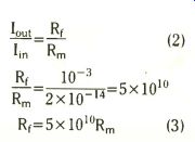
Mosfets are highly susceptible to break down of their gate insulation, due either to voltage transients or to static charges received through handling. Breakdown due to voltage transients is a major problem in instruments employing ionization chambers, since these often require polarizing potentials of several hundred volts. It is therefore essential to protect the input gate with devices which break down or avalanche non-destructively at a voltage lower than that which causes destructive breakdown of the gate insulation, and for less stringent applications zener or avalanche diodes are used for this purpose. However, for electro meters, the conductance of normal zener diodes would be unacceptable and special low leakage "pico-amp" diodes are used. The simplified input stage of a typical electro meter amplifier is shown in Fig.3.
The gate-protection diodes are connected between the vulnerable input gate and the common 0V line. In view of the requirement for negligible leakage, it might seem surprising that the diodes are connected in parallel and apparently short circuit the input terminal to zero. However, the pico-amp diodes are of very small area and are characterized by very low reverse leakage in comparison with ordinary signal diodes. This property, in conjunction with virtual earth operation, ensures that leakage current to common 0V is very small in comparison to the input current for the most sensitive range, irrespective of whether the diodes are for ward or reversed biased; provided, of course, that there is negligible voltage offset at the input terminal. However, the diode leakage approximately doubles for every 7°C temperature rise and consequently a 20°C rise might result in an eight-fold increase. With the input terminal at zero the magnitude of this increased conductance is not excessive at the elevated temperatures but, as discussed in connection with the choice of range voltage Vm for the most sensitive range, it can be accompanied by a voltage offset of 2mV.
Taken together, these effects of increased temperature can result in unacceptable offset current and it is therefore necessary to make provision for precise adjustment of the ‘Set Zero' control to minimize voltage offset, particularly at high ambient temperature.
The Set Zero control, shown in Fig.3, compensates for differences between the gate-source voltages for the mosfet pair when I of=0: it is adjusted in a Set Zero position of the range-selection switch, which short circuits the high-value resistor Rf and selects a lower value Vm. The control is normally a ten-turn potentiometer which, in conjunction with a Vm of the order of 10mV, permits the voltage offset to be easily maintained within ± 100µV of 0V.
In view of the fact that leakage through the protection diodes is rendered insignificant by virtual earth operation, why is it not practical to use bipolar transistors or junction-gate field-effect transistors (jug fets) in the input stage? The answer to this question is that the internal leakage current, that is current to and from the input terminal from the other electrodes, is too great in these devices. In mosfets, internal leakage is minimized by the gate insulation to a level many orders below the base current for a bipolar transistor and several orders below the leakage across the reversed biased gate junction of a typical jugfet. Even when mosfets are used, it is advantageous to minimize offset current with equal gate-to-source and gate-to-drain voltage, under which condition the internal leakage currents depicted in Fig.4 tend to cancel. This balanced operation also cancels external inter-electrode currents due to leakage across the header, which can be minimized by installing the electrometer amplifier within a desiccated, sealed compartment and using devices having headers of low-leakage glass.
Some years ago GEC-Marconi marketed an electrometer dual mosfet (MBH1) with a header assembly having inter-electrode guarding by means of an earth-plane. Unfortunately this device is no longer available and matched dual mosfets are now difficult to obtain, semiconductor manufacturers finding the market too small.
However, Intersil market a complete electrometer operational amplifier (ICH8500A) which is suitable for all but the lowest-current applications without selection and which embodies the essential features discussed in the foregoing text.
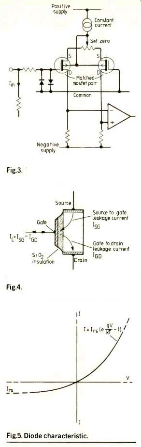
Fig.3. Typical input stage using mosfets and protection diodes.
Fig.4. Internal leakage paths in a mosfet, which tend to cancel when balanced.
Fig.5. Diode characteristic.
LOGARITHMIC ELECTROMETERS
For some applications of electrometer amplifiers, a single-range logarithmic display is an ideal way of presenting measured data, particularly for process-monitoring applications, where a wide dynamic range may be displayed on a strip-chart for 'at glance' interpretation. Freedom from the disturbances attendant upon range switching operations are added advantage of alb mode of operation.
It is well known that, if the feedback resistor of the conventional operational amplifier circuit is replaced by a junction diode, the amplifier output approximates to the logarithm of the input signal and it ma) be of interest to see how this principle it applied to our projected electrometer amplifier.
Figure 5 depicts the typical semiconductor diode characteristic; a simplified express ion for this relationship between applied voltage and the resulting current is I =lrs(e1-1) I= reverse saturation current where
V = applied voltage
q =electron charge
k =Boltzmann's constant
From this expression it can be seen that when V = 0, I = 0 and when V 60mV, it may conveniently be further simplified to v Im IrseT at normal ambient temperatures.
Taking logs of the revised expression, log eI=logelrs+1 and hence
V=kq logl-kq loglrs
As the last term is constant at constant temperature, dV/dlog I=kT/q
At 300°K this gives a figure of approximately 60mV per decade: a relationship which holds for perhaps ten decades determined by the physical dimensions of the diode.
Normal signal diodes are unsuitable at the minute currents measured by electrometer amplifiers and it is common practice to use a high HFE small-signal transistor as the feed back element as shown in Fig.6. In this arrangement I,,, =1,, which closely approximates to Ie if HFE is high and constant. As with the linear amplifier, external leakage is minimized by the use of a transistor of small area and, for this reason, the transistor is often reversed to make its emitter the input terminal, it being the smaller electrode in epitaxial devices.
The lower level of input current to which the logarithmic relationship extends is determined by the external leakage and by recombination current within the transistor, and few discrete devices are suitable at femto-amp levels. However, some of the very small geometries used for l.s.i. microcircuits, for example the Ferranti CDI process, are well suited to the application.
The upper limit of the input current range is determined by ohmic resistance, which only becomes significant at current levels well above our projected maximum, even for devices of such small size.
One interesting outcome of the use of a three-terminal logarithmic feedback element is that the output voltage is essentially unaffected by input offset-voltage variations of the operational amplifier: that is, there is no voltage drift due to this cause. However, the logarithmic response can be distorted at low current resulting from the voltage offset, which must therefore be as small as possible.
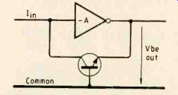
Fig.6. Replacing the feedback resistor by a junction diode provides
a log response.
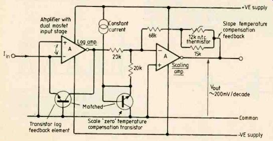
Fig.7. Circuit diagram of complete log amplifier with linear stage to
drive a recorder. Second transistor compensates for temperature characteristic
of feedback transistor.
Referring to the preceding paragraphs in which the parameters of the logarithmic response were discussed, it will be seen that the output voltage (Vbe) will range between approximately - 60mV and - 400mV over the five-and-a-half decades of Input current.
This is insufficient to drive a strip-chart recorder efficiently and further amplification is necessary. The following linear scaling amplifier also facilitates back-biasing to `zero' the recorder for the lowest current to be measured and the means for compensating the temperature dependence of the feedback element.
Temperature effects. If Vaat is plotted against logy Ii, the curve produced will of course be a straight line over the range of input current for which the logarithmic relationship holds; the slope of the line being 2.3026 kT/q volts per decade, as previously derived. Thus, the slope varies directly in accordance with absolute temperature. To compensate for this temperature dependence, the gain of the scaling amplifier is made to vary inversely with temperature.
------------
Also see: Double-notch filtering simplifies distortion analysis
==========
(adapted from: Wireless World , Jan. 1987)