AMAZON multi-meters discounts AMAZON oscilloscope discounts
In this section, we will complete the bridge from hardware to software by considering the role of microcomputers in digital design. We assume that you have some experience in programming a microcomputer at the assembly language or machine language level. From the programming viewpoint, microcomputers are small-scale versions of larger computers; given enough time and resources, any microcomputer can execute any algorithm. In this section, we will confine the discussion to the use of microcomputers to control digital devices.
In Section 10, we developed primitive microprogrammable computers specialized to emulate algorithms of a specific form. Their basic command implemented an ASM state with a conditional branch. In many cases, there is no need to use such a specialized computer, since any computer is a universal algorithm emulator when properly programmed. Of course, some computers may be a poor choice for certain design problems, because of an ill-adapted instruction set, inadequate speed, unsuitable input-output facilities, or high cost.
In digital design, the microcomputer can often serve as the controller the executer of the control algorithm. In earlier design methods used in this guide, we maintained direct and intimate contacts between the controller and the controlled devices; the processing of status signals and command outputs was flexible, with a high degree of parallelism. The relationship of a microcomputer controller to its environment is quite different and more restrictive, and the control algorithms must abandon much of the former parallelism. We will devote most of this section to these aspects of microcomputer-based design. But first, a bit of history will show how ordinary computers came to be used in digital design.
THE COMPUTER AS A DEVICE CONTROLLER
The first computer widely used as a controller of hardware was the PDP-8, primarily because it was the first computer whose price was less than astronomical.
The history of the PDP-8 sheds insight on the evolution of microcomputer-based design. In the early 1960s, a group of engineers was assigned to build a controller for a nuclear reactor. The reactor supplied status signals such as neutron flux, core temperature, and power output. The primary controller commands were directed to motors that inserted and withdrew cadmium rods that absorbed neutrons and thereby controlled the reactor power. The initial design of the controller was hardwired. Unfortunately, the problem was incompletely specified, since the reactor was still under construction. The algorithm changed often, and each change required that the designers rip out gates and wires and start anew.
The conviction gradually arose among the engineers that they must seek a general solution that could handle all the cases then known and the likely new ones to come.
What characteristics must such a device have? It must be an arbitrary algorithm emulator. The algorithm may involve computation as well as control.
For example, the motion of the control rod may be a complicated mathematical function of power output and neutron flux. Speed was of no particular importance, since the inertia of the control rods would limit the mechanical responses to milliseconds, regardless of the speed of the controller.
There were two ways to meet these requirements:
a. Extend the controlled architecture (the reactor) to include primitive arithmetic units, registers, and memories to support the computational requirements.
The control algorithm would then manipulate these elements to perform computations as well as control the cadmium rods. This is a hardwired approach, using more powerful and general architectural elements such as bit slices that allow the handling of more general classes of algorithms.
b. Use a conventional computer to emulate the algorithm. The reactor would be interfaced to the computer and treated as a peripheral device that received commands from the computer and supplied status signals in return. At that time, all computers were expensive, and were difficult or impossible to connect to so strange a device as a reactor.
One way to meet the design" goals was to design and build a small, inexpensive computer with sufficient flexibility to allow easy interfacing of arbitrary peripheral devices. In an inspired decision, the engineers chose this approach, and the PDP-8 was the result. This early PDP-8 was crude by later standards, but it worked! A steady stream of new minicomputers followed, as manufacturers hastened to develop small computers priced to encourage their use in process control and automation applications.
Enter the Microcomputer
In the early days, minicomputers were made with integrated circuit logic of the MSI level of complexity. Minicomputers had lots of chips; the more elaborate minicomputers can have chip counts exceeding one thousand.
The VLSI technology that emerged in the late 1970s led to placing more and more circuitry on a single integrated circuit chip. With the introduction of the Intel 4004 microprocessor chip, the microcomputer revolution was under way. A microprocessor is a complete computer instruction processing unit on a single chip. Add a memory and a method for input and output of data, and you have a microcomputer.
These devices differ from their large computer and minicomputer counterparts in many details, but in their basic approach to problem solving they remain conventional computers. It is their incredibly low cost that sets them apart; price, not concept, is the reason for the explosion of uses of microcomputers.
A microprocessor chip can cost only one dollar; a microcomputer with mounted microprocessor, memory, input-output components, power supply, and cabinetry can cost as little as a hundred dollars. Common abbreviations for the microprocessor are MPU and CPU.
THE MICROCOMPUTER IN DIGITAL DESIGN
The technical community now has much experience in using computers to solve a wide variety of problems. Our interest is in digital design: how do we use a conventional computer (a minicomputer or a microcomputer) as an element of hardware design? A computer is a general algorithm executer, so it would seem reasonable that computers may be able to perform the control portion of suitable designs.
This approach brings our view of the design of a controller much closer to conventional programming. We express our control algorithms in a computer assembly language or perhaps in a high-level language such as Fortran. The conventional computer greatly restricts the ways in which a designer can access the controlled device. The hardware view of testing continuously available variables gives way to a computer program that directs the computer to read status information from the controlled device into the computer for later testing. The conditional branch of the ASM becomes a step in a conventional software flowchart, or a high-level statement such as
IF (STATUS) THEN ... ELSE ...
The parallel activities in an ASM state become a sequence of steps in a computer program. Commands to a controlled device take the form of write statements.
There remains little sense of the detailed hardware timings that characterized our earlier methods of control.
We retain the underlying model of a controller as directing a controlled device (the architecture), but our view of control is quite different when using the microcomputer than when using hardwired or microprogrammed control.
Here is a comparison of the three approaches:
a. Hardwired control. The fastest emulation of an algorithm, with its speed limited by gate propagation delays. The ASM chart is the most convenient way to display algorithms. Multiway branches and conditional outputs can reduce the number of states, allowing many operations to proceed in parallel, further enhancing the speed of the circuit. In systems with up to about 16 states, this method is simple enough to be our choice. The cost of components is minimal, but fabrication and debugging are laborious, and errors in design or implementation result in tedious alterations of the hardware.
b. Microprogrammed control. Slightly slower than hardwired control, its speed is still limited by propagation delays. The slowdown results from the extra states required by multiple branches and conditional outputs. Microprogrammed control is most suited to complex algorithms, say with more than 16 states, and is limited by the address space of the control store and by the management of the complex algorithms. Microprogram designers need high-level design aids such as the Logic Engine. The cost of the production version of a microprogrammed control is small.
c. Conventional microcomputer control. The method of choice when slow speed and somewhat higher cost are acceptable. Speed is generally 10 to 100 times less than in the two previous methods, because of two characteristics of computers. The basic time unit is that of a computer instruction, which requires several clock cycles, whereas hardwired and microprogrammed controllers execute a state in one cycle, and the execution of a state requires several instructions. The reading of status variables or the writing of command outputs requires one or more separate instructions, as does the testing of status variables.
Offsetting these restrictions is the excellent human interface accompanying most computers, including microcomputers. The basic expression of the algorithm is the program, perhaps with the aid of a software flowchart. Complex computer programs, whether for control or for general problem solving, require considerable software support. Loaders, editors, assemblers, and operating systems are necessary, and we expect these facilities to accompany the computer hardware.
Still, after a microcomputer-based control design is complete, you may often remove from the production version much of the equipment that supported the development.
Microcomputer control of a digital system can replace much of the control hardware with software, but the architecture remains "hard." The controlled device is frequently some existing piece of equipment, around which we construct sufficient hardware to adapt it to the requirements of our microcomputer system.
DATA FLOW IN A MICROCOMPUTER
The severe limitation on the number of pins in a microprocessor chip means that there is usually only a single data path into and out of the chip. Instructions and data from memory, output to peripheral devices, and all other transfers of data into or out of the MPU occur over this one path, called the data bus.
Remember, a bus is a data path consisting of a set of signal paths or wires, one wire per bit, over which many components may send or receive information.
The data bus is usually as wide as a memory word-8, 16, and 32 bits are typical sizes.
To direct the flow of information into and out of the microprocessor, two more busses emerge from the chip: an address bus and a control bus. The address bus designates the destination of a data transfer; since all data moves over the data bus, the microprocessor will use the address bus not only 10 describe memory locations but also to designate the peripheral devices attached to the system. This bus is usually 16 or 24 bits wide. The control bus determines the direction of information flow; input from the addressed device or output to it.
The structure of the control bus varies. A simple-control bus might have just two lines, a read line for initiating inputs to the microprocessor, and a write line for starting output operations from the microprocessor. Most control busses have additional signals for managing timing and interrupts.
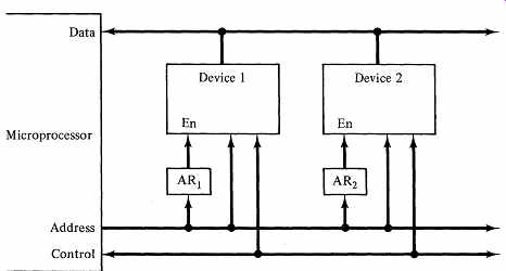
FIG. 1. The bus structure of a microcomputer. Each device has an address
recognizer AR.
Memory references are the most frequent use of the microprocessor busses.
To retrieve a word from the memory, the MPU must place the proper address on the address bus and then place a read signal on the control bus. The memory must have enough internal logic to recognize the read signal, accept the address, and start a read cycle that will eventually place memory data on the data bus so the MPU can accept it. The MPU performs a write operation by placing the address, the MPU data, and a write signal on the proper busses; the memory must accept all this information and perform the memory write operation.
The microcomputer's memory, terminal, and mass storage share the bus with other devices. FIG. 1 is a generalized microcomputer bus. Each device has an address recognizer, which scans the address bus and asserts an enabling signal whenever the bus contains an address associated with the device.
The address recognizer is usually a simple combinational circuit, whose details vary with the microprocessor's addressing scheme and the addresses assigned to the device. Two addressing schemes are in common use. We may divide the activities of a microprocessor bus into memory accesses and input-output transfers. In a microcomputer system, these two bus activities may be separate concepts or manifestations of a single concept. In systems where memory and input-output are conceptually separated, we speak of the separate input-output approach; the concept of unified memory and input-output is called memory mapped input-output.
Memory-Mapped Input-Output
In memory-mapped input-output, every device attached to the system behaves like a memory location with an address. In a microprocessor designed for this approach, we input a byte from a terminal keyboard by executing a load instruction, just as we would to obtain the contents of a memory location. The load instruction has an operand address that identifies the particular device. Outputs arise through store instructions; there are no read or write instructions. A data transfer causes the address to appear on the address bus, to be interrogated by the address recognizers in all devices (including the memory). The selected device recognizes its address; then, governed by the control bus signals, the device transmits or receives information over the data bus.
Memory-mapped input-output is elegant, simple, and flexible. The necessity of decoding the large address field is only a minor drawback. Many microcomputers use this approach: the Motorola 6809 and 68000 series are popular examples.
Separate Input-Output
The separate input-output strategy incorporates two bus systems, one for memory and a separate one for input-output devices. Peripheral devices are attached to the input-output bus, and the RAM goes on the memory bus. These microprocessors have read and write instructions for input and output. The Intel 8080 has a separate input-output system.
Since the microprocessor chip itself has only a single data, address, and control bus structure, there must be extra hardware outside the chip to route the microprocessor bus information onto the correct external busses. In this method, the microprocessor has a select signal in its control bus to specify which of the external bus systems to use. This signal allows the decoding hardware to enable the address, data, and control signals onto either the memory bus system or the input-output bus system.
Since the decoding hardware has separated the memory references from the input-output, the memory unit does not need to do further decoding to identify memory addresses. Similarly, the input-output address bus transmits only the addresses of peripheral devices, not memory addresses, so the address recognizers in the devices are usually simple. Because there are far fewer peripheral devices than memory words, the input-output address bus may be much smaller than the memory address bus: 8 bits allow for addressing an ample number of peripherals.
Separate input-output is less flexible than memory-mapped input-output, but the separation of memory and input-output functions seems more natural to some people. Either scheme is satisfactory, and the designer sees little fundamental difference between them.
Device addressing. To each device one or more unique addresses are assigned. They may be permanently assigned and built into the device or they may be selected with switches on the device's cabinet. A printer may have only a single address, whereas a RAM would respond to a host of addresses corresponding to each word in the memory. All devices monitor the address bus lines, and respond only to their particular addresses.
Few devices have suitable circuitry for recognizing addresses built into them. If you are using the microcomputer as a controller for a piece of "foreign" equipment, you will have to interface the controlled device to the microcomputer controller. By using the methods described in Sections 2 and 3, you can design efficient MSI address detection circuits, using gates for a fixed address or arithmetic magnitude comparators for a selectable address.
Suppose the devices in Fig. 1 are assigned the following 16-bit addresses in a memory-mapped system. The addresses are given in hexadecimal notation; bit A 15 is most significant and bit A0 is least significant.
Device 1: Address F002
Device 2: Addresses F004-F007
In Device 1, the address recognizer ARI must implement the equation:

Device 2 has a range of four addresses. All combinations of the least significant 2 bits are valid, so address recognizer AR2 must implement:
Hardware for the Bus Interface
The interface of a component to a bus is called bidirectional if the device can both send and receive signals, and unidirectional otherwise. For instance, RAMs have a bidirectional interface with the data bus and a unidirectional (input only) interface with the address bus. An MPU has a bidirectional interface with the data bus and a unidirectional (send only) interface with the address bus.
Most busses in microcomputer systems rely on three-state control, as observed in Section 3. Microcomputer components are low-power devices, yet many components may be attached to the bus as receiving circuits. To provide adequate power for reliable bus operation, it is often necessary to buffer the outputs onto the bus. For unidirectional outputs, three-state buffer chips such as the 74LS244 Octal Buffer are useful "drivers." Most logic inputs may serve directly as unidirectional bus receivers.
For bidirectional bus attachments, in which a single pin of a device must carry both input and output data, we may use a three-state bus transceiver, shown in Fig. 2. To operate such a device, we send control signals to specify whether the transceiver is to transmit, receive, or do neither. This requires two control lines as in Fig. 2a. Often a single control line for the transceiver is sufficient, in which case the transceiver always passes data in one direction or the other, as in Fig. 2b. In some LSI chips in microcomputer systems, bus transceivers are built in; others require separate circuits.
Part of the task of interfacing a device with a computer is to manage the system bus's transactions. This requires detailed adherence to the timing and format of the particular bus system. Many manufacturers provide support hardware to make this task easier at the peripheral end. Typical of this are special LSI chips with names such as input-output ports and peripheral interface adapters (PIAs). These chips are versatile, often managing 16 bits of parallel data in elaborate configurations determined by programming. PIAs have registers and buffers for the input and output of data, status and control signals for handling bus activities and peripheral timings, some address decoding capability, flexible support of interrupts, and other useful features. The microcomputer program establishes the complex operating conditions of the PIA by programming the contents of the PIA's control registers.
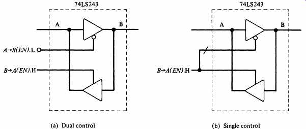
FIG. 2. A bus transceiver in two configurations.
Bus Protocols
If you are attaching a device to a microcomputer, you must be thoroughly familiar with the bus control protocol of that system, whether you design the protocol yourself or use an established one. Bus protocols are more complex than those shown here. There are many protocols in use, including quite a few promulgated by manufacturers or technical groups. Several such "standard" protocols have gained favor, although not all of them are well conceived, nor are they completely standardized. Still, when it is possible, use a standard protocol rather than creating your own.
MICROCOMPUTER INPUT-OUTPUT
To the digital designer, a microcomputer program represents a control algorithm; the program issues commands and receives status information by means of input and output operations directed to the controlled device. Usually the microcomputer is dedicated to the task of device control, and the microcomputer program controls every aspect of the architecture's interface with the system. The technique for this detailed control is called programmed input-output, which can be used either with or without interrupts.
Programmed Input-Output
Programmed input-output is a simple and versatile scheme supported by every microcomputer. The MPU program explicitly controls the transmission or receipt of each byte of data passed over the data bus; thus the name programmed input output. Usually, the program uses one of the MPU's registers to hold a byte of outgoing data or to receive an incoming data byte. MPU input-output instructions cause transfers between the MPU's register and the system data bus; these instructions are the loads and stores of memory-mapped input-output or the reads and writes of separated input-output.
Since the only data connection between the controller (the MPU) and the controlled device is the system data bus, command outputs from the controller take the form of a byte of data sent out by an MPU output instruction to the addressed device. The device may interpret one or more of the bits in this byte as control signals or may use the information as data, as specified by the designer.
If the device requires more data or control information than one byte can hold, the designer must assign additional addresses to the device, providing another "home" for command information, or to process bytes of control information serially.
The controlled device usually generates status information to guide the control algorithm in the MPU. These signals do not influence the MPU's activities the instant the device develops them, since the MPU must issue a programmed read before the device is allowed to place the status information on the data bus. After the status data is in the MPU, the program tests the status as a part of its execution of the control algorithm.
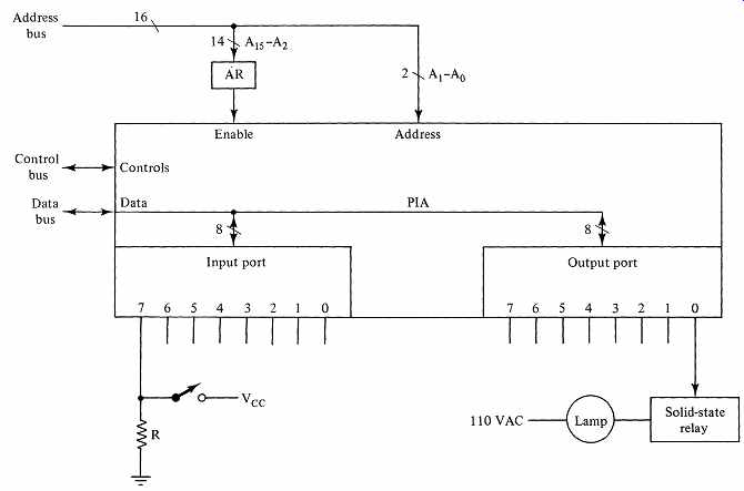
FIG. 3. A switch operating a lamp, controlled by programmed input-output
through a PIA.
Here is a simple example of microcomputer control using programmed input-output. We wish to turn on a light in response to a switch. We use a PIA to sense the setting of the switch and to maintain the control signal that governs the light. Our model for this example is the Motorola 6809 system, which has an 8-bit data bus and a 16-bit address bus. By software, we specify an 8-bit input port and an 8-bit output port in the PIA, as shown in Fig. 3. The switch is connected to the most significant ("sign") bit of the input port, and a relay that controls the lamp is connected to the least significant bit of the output port. (In Section 12 we discuss how to drive relays.) This exercise requires only these 2 bits.
We assign the address F008 (hexadecimal) to the input port and FOOA to the output port. In response to either address our address recognizer asserts an enabling signal to the PIA. PIAs usually have several addressing inputs to distinguish between the chip's internal registers. We will attach the two least significant address bus lines A1 and A0 to the PIA's addressing inputs. Our address recognizer, working with the most significant 14 bits of the address bus, identifies the PIA as the target, and the remaining two address bus lines tell the PIA which register is being addressed.
In Fig. 4 we present a section of 6809 assembly-language code for the control algorithm. You can understand this simple program without knowledge of the 6809. LDA and STA are load and store instructions, which in this memory mapped system are used to address the ports of the PIA. BPL and BMI are branches on plus and minus, respectively. JSR is a subroutine jump, and CLR is a clear or "store zero" instruction. EQU is the usual symbol-equivalencing assembly directive.
The code performs a software switch-debouncing action by pausing sufficiently long after detection of a switch transition. A valid change in the switch setting prompts the turning on or off of the light, and spurious switch signals evoke no response.
[...]
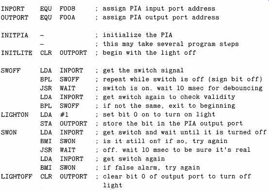
FIG. 4 Programmed control of the architecture in FIG. 3.
The architecture of the interface circuitry and the spirit of the programmed control of more complex designs are similar to this simple example.
Programmed Input-Output with Interrupts
Some types of peripheral interactions are sporadic and unpredictable. Keyboard entry from a low-speed terminal is an example: A user may depress a key the next second or not until next week. To control such a device with normal DMA or programmed input-output, we would execute a loop that tested the status of the keyboard device frequently, waiting for a character to come along. This straightforward approach is acceptable if the MPU does not have more pressing business, but in busy systems this may use up too much time.
Most microcomputers support external interrupts. This feature requires an additional line on the control bus: the interrupt request signal. When the MPU senses that the interrupt request line is true, then at the end of the next instruction the MPU forces a subroutine jump to a special memory location set aside for this type of interrupt and begins executing the instructions located there. The programmer arranges for a suitable interrupt subprogram to reside in memory, beginning at the special interrupt location.
The interrupt subprogram must determine the reason for the interruption of normal processing, and take appropriate action. For example, consider the processing of character data from a terminal keyboard, using interrupts to announce the availability of a character. The MPU program goes about its main business, for example, monitoring the status of temperature and pressure sensors in a chemical process and controlling a heater and a vacuum pump motor. The main MPU program takes no heed of the keyboard, which is present only for an occasional human intervention. When the experimenter presses a key on the terminal, the terminal's interface hardware asserts an interrupt request. This causes the MPU to suspend the execution of the program and make a subroutine call to the interrupt location. There, the interrupt subprogram determines that the reason for the interrupt is the availability of a character from the terminal.
The interrupt subprogram reads the character, using programmed input, and deals appropriately with the character. The subprogram then does a subroutine return, which causes control to return to the next instruction following the original point of interruption. If the interrupt program has been properly written, all the relevant registers of the MPU will be unaffected by the interruption and the interrupted program will not be aware that the interrupt has occurred.
As you learned in Section 7, computers always provide a way to turn the interrupt recognition hardware off and on, so as to give the MPU program some control over its operating environment. There are two situations in which we want the interrupt recognition system to be turned off: when the algorithm is not designed to handle any interrupts, and when the interrupt subprogram is already dealing with an interrupt. This last case is interesting; it arises to avoid the possibility of one interrupt piling on top of another one.
In the simplest form, the entire interrupt detection structure would be inactive during the processing of an interrupt. A more sophisticated method is available in many microcomputers. The priority interrupt scheme provides hardware support for prioritized levels of interrupts. Here, the designer assigns each type of interrupt request a priority level, with interrupts requiring rapid processing having higher priorities. An interrupt occurring at a particular priority level will disable detection of all interrupt requests of equal or lower priority but will preserve the ability to detect higher-priority requests. In such a system, each priority level has its own interrupt location in the memory, which must contain the start of an interrupt subprogram capable of dealing with the interrupt. During the processing of an interrupt request at a certain level, if the MPU detects a higher-priority request, a new interrupt subroutine jump will occur.
It sounds tricky, and it is. Interrupts are potent tools for providing service on demand, but they cause a host of difficult problems.
Difficulties with interrupts. Interrupt programming is much more difficult than ordinary software development. The trouble is that interrupts are not re producible. The time of an interrupt request is not under the direct control of the MPU; interrupts do not occur in lockstep with the MPU algorithm. It is an intrinsic property of the interrupt concept that we cannot predict exactly when an interrupt will occur. Most complex programs have weak, perhaps little used, sections that have not undergone rigorous testing. It is difficult to test an interruptible program thoroughly. An interrupt may occur during a section of the program that is not correctly written for interrupt processing. For instance, the main program must be careful in using memory data that an interrupt subprogram might also use. Might is the key word; an incorrect program may run for a long time without an interruption in the erroneous section. Such nonreproducible errors are nearly impossible to diagnose after the fact. And creating flawless programs in an interrupt environment is orders of magnitude more difficult than in simpler circumstances.
Since interrupts can occur between any two instructions of an executing program, the interrupt subprogram must be written with great care. Its execution must leave no effects that might disturb the correct execution of the interrupted program. In particular, the interrupt subprogram must not alter the MPU's operating registers, or at least must restore these registers to their original state before returning to the interrupted program.
Of course, the interrupt subprogram will make some change in the state of the computer system; otherwise, why bother detecting the interrupt? Usually, the subprogram will store some information in the memory, or initiate a new input-output activity. Programmers must design their programs with great care, so that they perform flawlessly even in the presence of unpredictable interrupts.
Interrupts are the software equivalent of asynchronous hardware circuit design. Both are powerful techniques loaded with opportunities for errors. In hardware, we found that synchronous design allows simpler handling of most problems, with little or no penalty. This was possible primarily because in hardware and in microprogramming we may perform many operations in parallel and can thereby achieve great overall speed whether or not the design is clocked.
In conventional computer software, each instruction performs only a small task and activities are highly serial. Serial processing is slow. We need any facility that can help speed performance and enlarge the spectrum of problems amenable to conventional computer processing. We cannot forego interrupts as easily as we sidestepped asynchronous design.
So interrupts are often necessary, but you must always be aware of the design and debugging problems introduced by this powerful concept.
DESIGN EXAMPLE 1: A WIRE-WRAP CONTROLLER-PURE SOFTWARE CONTROL
Printed circuits, wire-wrap, and wire plugboards are common ways of fabricating digital circuits. Plugboards-special connector boards with holes into which the designer pushes wires-provide a manual method suitable for testing small prototypes. Printed circuits are best for high-volume production but require substantial efforts at circuit layout and fabrication. Wire-wrap serves a wide range of applications, including testing prototype of large circuits destined for printed circuits and production versions of circuits of varied complexity.
In wire-wrapped circuits, integrated circuit chips are plugged into mounted sockets having special wire-wrap pins. Electrical connections are made through wires strung between pins and wrapped to each pin by means of a wire-wrap tool or "gun." Wire-wrap is inexpensive, and commercial products such as insulation stripping tools, wrapping tools, and sockets are plentiful. Wire-wrapped circuits are easy to modify in the field.
Manual wire-wrapping is feasible, but in a large circuit the forest of pins and wires confuses the eye and leads to occasional errors. Locating the correct pins is tedious and slow, a likely candidate for automation. Fully automatic numerically controlled wire-wrap machines are commonplace in high-volume production plants, but these machines are expensive and require elaborate setting up.
With a more modest investment, using commercial equipment, we can develop a semiautomatic wire-wrap facility. The system relies on a human operator to wrap the wires but provides for the automatic positioning of a guide for a wrapping tool so there is no doubt about a pin's proper location. The equipment consists of a wire-wrap table and its controller. In the following example we use a commercial wire-wrap table and a microcomputer for control.
The Architecture
The wire-wrap table is an upright X-Y positioner with a rigid rectangular frame that holds the board to be wrapped. On the frame is mounted a vertical beam that can move in the horizontal (X) direction along a precision screw. Attached to the vertical beam is a smaller beam that can move along another precision screw in the vertical (Y) direction. This smaller beam holds the guide for the wire-wrap tool. By a suitable combination of motions in the X and Y directions, the controller may place the guide at any location within the rectangular frame.
Each beam has a stepping motor that can position the beam precisely by rotating the screw. A stepping motor responds to a control pulse by moving one step in a specified direction. In our system, a motor step results in a beam movement of 0.005 in.; thus there are 200 beam steps per inch. To move a beam 5 in. would require 1000 properly administered steps.
The stepping motors are independent, so both beams may be in motion at the same time. Each stepping motor has a driver that responds to digital TTL control signals and converts them into high-power motor signals. In our example, each stepping motor control has a direction signal (specifying left or right; up or down) and a motor signal. To move a beam one step, we establish the proper value of the direction signal and then make the motor signal true for a specified time (about 1 msec). At other times, the motor signal must be false.
Starting from a resting position, a stepping motor may reliably begin motion at a rate of up to 200 steps per second; once in motion, the motor may be gradually speeded up to 600 steps per second. For reliable operation, the stepping must be decelerated to a maximum of 200 steps per second before the motor is brought to a halt. Stepping the motors too fast can result in lost steps. The manufacturer specifies the desirable rates of increase and decrease of the stepping speed.
Specifications for the Controller
The wire-wrap table is ideal for microcomputer control:
a. It is slow. Almost any microprocessor can drive the stepping motors at full speed and can easily keep up with the human operator.
b. The control is a complex task, easily handled in software, yet difficult for a pure hardware controller.
c. The design is likely to change as our experience suggests minor modifications.
d. We can use the microcomputer's interface with the operator to good ad vantage. A display terminal, floppy disk, editor, and assembler will assist the development task and may later become part of the production system.
The wire list. The wire list contains the basic data for wire wrapping.
Each wire connects two pins; the wire list gives the pins' location in terms of X and Y coordinates relative to an arbitrary origin. For convenience, each entry in the wire list contains the length of the wire and a commentary to assist the operator to identify the wire.
The designer prepares the wire list before wrapping a board. There are several devices commonly available in microcomputer systems that can retain the wire list: paper tape, floppy disk and hard disk. The floppy disk is the most versatile.
The operator's controls. The operator should have a foots witch to signal the controller that a wrap has been completed and the wire-wrap tool is removed from the guide.
A small keyboard with 10 or 12 buttons is a convenient way to enter information into the controller. The keyboard has two basic functions; the panic button, which will cause the immediate halting of the stepping motor, and a set of four buttons to permit manual movement of the table beams. The operator can press anyone of the four buttons - X, + X, - Y, or + Y to move the guide in the indicated direction. If the operator holds a button down longer than 0.2 sec, for example, the controller moves the beam at a rate of 200 steps per second until the button is released. Single steps result fwm depression of less than 0.2 sec.
Another keyboard button can cause the computer to position the wire-wrap guide at the point the controller believes to be the origin. This is useful to verify that the stepping motors have not missed steps during previous wrapping operations.
We may design additional operator controls to be entered either from the keyboard or from the microcomputer's main display terminal. For example, it is useful to allow the operator to search the wire list for a given wire which can serve as a starting point for wrapping operations. This need arises when an operator has suspended wrapping and wishes to begin again.
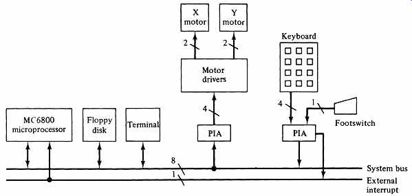
FIG. 5. Signal paths for the wire-wrap controller.
The controller. Any microcomputer can control the wire-wrap table. We might choose a Motorola MC6809 microprocessor with 32K RAM storage, a floppy disk, and a display terminal. This machine has memory-mapped input output for communication, and supports external interrupts. A peripheral interface adapter (PIA) provides a convenient interface between the wire-wrap table's motor drivers and the microcomputer. The PIA contains registers for data written from the microprocessor, so the control algorithm's responsibility is to enter proper signal changes into the bits of the PIA registers. FIG. 5 shows the logical interconnections of the microcomputer, its peripheral devices, and the wire-wrap components.
NEXT>>
Related Articles -- Top of Page -- Home