Figure 4-1.
| Home | Audio mag. | Stereo Review mag. | High Fidelity mag. | AE/AA mag. |
Although this section deals with simple systems, it does point the way to more ambitious projects.
Figure 4-1.
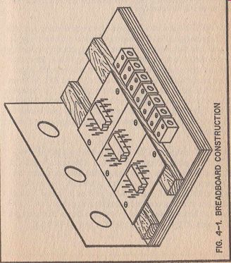
Figure 4-1 illustrates a method of "breadboard" construction used by the writer. It is really an adaption of the IC test-board already described in Section 3. A block of wood has two strips on which to mount Veroboards, and is fitted with a simple front panel to accommodate switches and controls as required. The assembly is completed by a multiway connector block.
Standard 2.5 x 1 inch copper stripped Veroboards having a 0.1 inch matrix comfortably take single 14 pin or 16 pin integrated circuits mounted direct or via holders. Veropins, suitably staggered, are used to provide connecting posts. The boards are secured to the two strips by small wood screws or captive nuts and bolts. Whatever method is adopted, the object is to be able to mount, remove or replace the boards easily.
The question arises of whether to fit the IC directly onto the Veroboard or via a holder. If the IC is a basic gate or device frequently used for experimental purposes, it is worth mounting it direct because the holder costs more than the and probably more than the IC. On the other hand, it is useful to have several mounted holders available for use with more expensive or little used devices.
Two NAND gates can be wired as a multivibrator, and this arrangement is ideal for many applications where a simple signal source is required. Figure 4-2 suggests a typical arrangement used as a signal injector for radio servicing. Since the square waves produced by the circuit are very rich in harmonics, the signal can be injected into IF and RF amplifiers as well as those working at lower frequencies. The method is to start at the output stage and work back towards the aerial end of the receiver. At each point the 1 kHz tone should be detected at the output, otherwise the last stage to be checked is suspect.
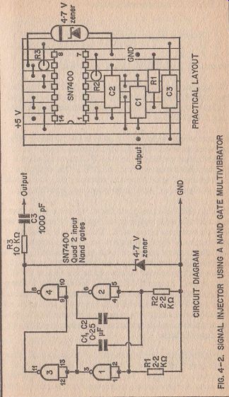
Figure 4-2
It will be noticed that the two gates not used by the multi-vibrator circuit are wired as buffers. It is good practice to buffer oscillators in order to stabilize the frequency the frequency and produce a better waveform, but in this application stages 3 and 4 can be omitted if desired. In any case, the isolation and protection circuit, comprising C3, R3 and the Zener diode, should be used to ensure that voltages in excess of 5 V are not accidentally applied to the IC.
The multivibrator frequency mainly depends on the values o f R1 , R2, C1 , C2 and approximates to:
10s frequency (Hz) = (C1R1 ) + (C2 R2) x 0.9 where C is in microfarads and R is in ohms.
The formula does not take into account other factors including external loads. I f a precise frequency is required, it is advisable to make both or one resistor variable within the range 2.2 k-o ± 25%.
The convenience of having four gates in one package is fully exploited in the tone generator illustrated in Figure 4-3. A multivibrator operating at about 800 Hz is switched by a second multivibrator operating at 22 Hz. The result is a combination of both frequencies producing the characteristic high pitched "burr" used in telephone and intercom sets.
I t will be seen from the circuit that the output is taken from across R4 to a high impedance loudspeaker. Alternatively the telephone earpiece can be used. This normally produces sufficient sound for the average room. I f the intercom has an amplifier, the tone can be fed to the input, thus making use o f the existing loudspeaker. Once again care should be taken to ensure that no excessive voltage can be fed back to the IC. This can easily happen i f the device is operating into a system using inductor--such as transformers and relays. If in doubt, use the protection circuit shown in Figure 4-2, although it will probably be necessary to increase the series capacitor to about 10 microfarads, and decrease the series resistor to a value not less than 470 ohms.
The multivibrator is just one method o f obtaining a rectangular waveform. Sometimes it is required to derive this shape from some other signal. For instance, many low-frequency sine-wave oscillators have a square-wave output facility, but the waveform is not good enough to drive a TTL system. The circuit shown in Figure 4 4 produces a good rectangular waveform from virtually any signal and makes the ideal input interface for TTL.
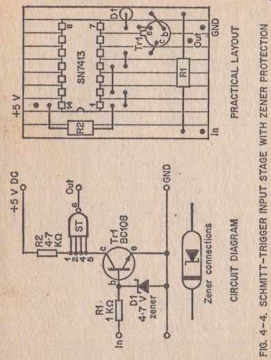
Figure 4-4
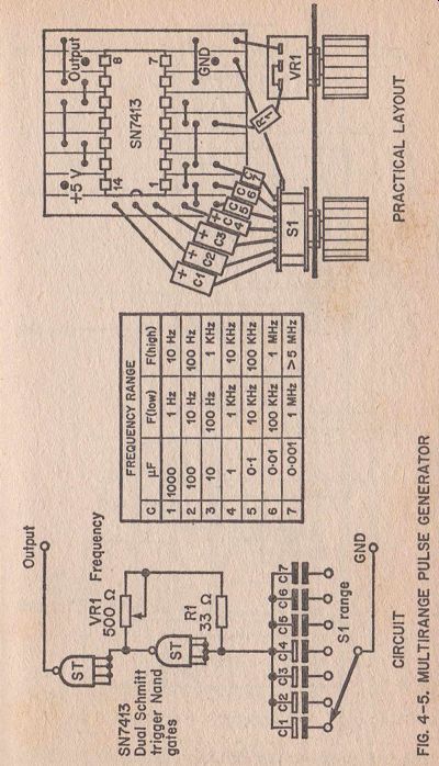
Figure 4-5
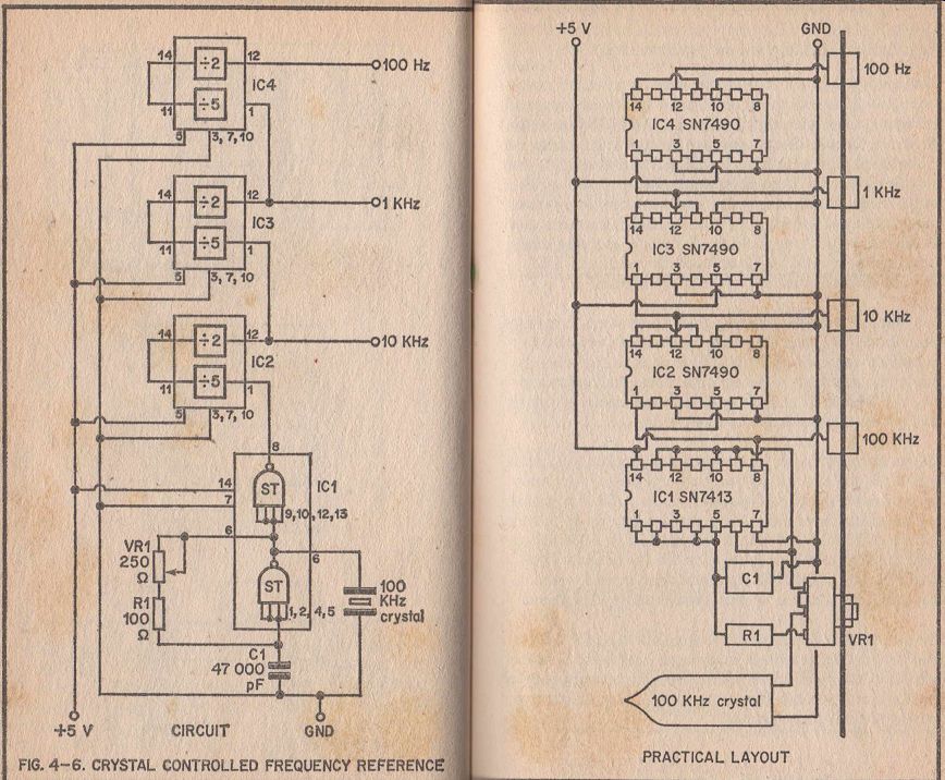
FIG. 4-6 . CRYSTAL CONTROLLED FREQUENCY REFERENCE PRACTICAL LAYOUT
It will be seen that an input transistor is used to hold the Schmitt-triggered NAND gate at the required level and, with R1 and a zener diode, protect the IC against excessive input signals. I f the device is to be used to feed circuits using high voltages, it will be desirable to provide output protection as well, and the arrangements discussed for the previous two circuits will normally be satisfactory.
Construction is straightforward, with a x 1 inch Veroboard again being used. but this time a second break is made in the copper strips to isolate the input transistor stage.
The Schmitt-triggered NAND-gate is also used in the multi- range pulse generator shown in Figure 4-5. The advantage of this arrangement over the circuit using a NAND-gate multivibrator is the wide frequency range obtainable from only one CR network. From the table it will be seen that the 500 ohm variable resistor VR1 gives a frequency swing of 10:1 on all ranges except the highest, so that seven switched ranges give continuous coverage from 1 Hz to 5 MHz. The circuit can actually be made to oscillate at 15 MHz by reducing the capacitor to about 47 pF, although the setting of VR1 becomes critical i f oscillation is to be maintained. .
Construction is simple, with the layout following the arrangement shown in Figure 4-1. Once again it will be necessary to provide output protection if the unit is to feed circuits employing potentials in excess of 5 volts. The constructor may also wish to fit a simple output potentiometer, although for logic circuits this is usually unnecessary.
The oscillator just described can be readily locked to a quartz crystal to provide a stable frequency reference. A suitable arrangement is shown in Figure 4-6, where a 100 kHz crystal controlled oscillator drives three decade counters to provide outputs of 100 kHz, 10 kHz, 1 kHz and 100 Hz. Since these outputs are rich in harmonics, they are an excellent signal source for the calibration of communication receivers and RF signal generators as well as low frequency equipment.
The system may be constructed onto four separate 2.5 x 1 inch Veroboards, or a single larger board can be used. In the latter case i t is necessary to interrupt the copper strips between the ICs as well as below them in order to isolate the stages and prevent the pins from shorting.
The frequency of the oscillator has to be adjusted until i t locks onto the crystal. The best way to do this is to arrange for the 100 kHz output lead to be near a radio receiver tuned to BBC Radio 2 on 1500 meters long wave. This is 200 kHz and a second harmonic to the required frequency. As VR1 on the reference oscillator is adjusted, the frequency will suddenly lock onto the 100 kHz crystal and its second harmonic will distort the radio signal. The frequency will then stay locked over a relatively wide variation of VR1, which should then be centered between the two non-lock points. The setting should be tested by switching the unit off and on several times to ensure that it always locks onto the crystal very quickly after switch-on.
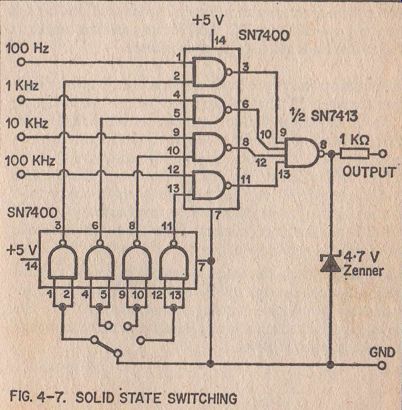
Fig. 4-7
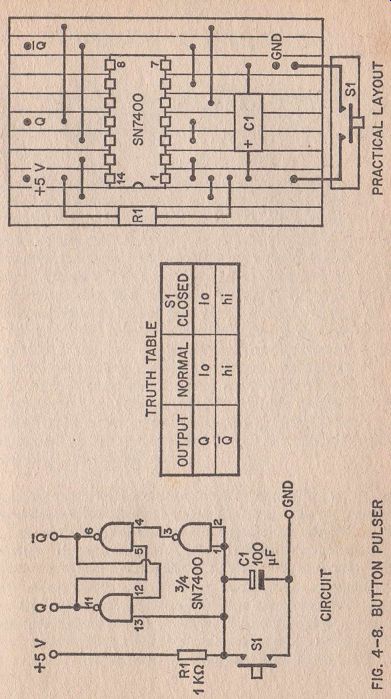
Fig. 4-8
If it is considered necessary to provide output protection, isolation can be provided by buffers, such as the four gates in a SN7400 package followed by the usual series resistor and Zener diode.
Some constructors may prefer to switch the different frequencies to a single output terminal. One method is illustrated in Figure 4-7. It will be seen that the four outputs are routed through NAND gates to the four inputs of the second Schmitt-triggered NAND gate. A further four gates, wired as inverters, are used as inhibitors. When their input is "hi" , their output is "lo" , and no signal may pass through the associated gate. The required frequency is selected by making the input of the appropriate inhibitor 'lo " . Solid- state switching allows a simple switch to be used, and because switching potentials are DC, there are no problems relating to long switch leads and high frequency losses.
The problems relating to switch noise is high frequency logic circuits such as TTL have already been referred to in Section 2. It will be recalled that the logic test set uses a single-pole changeover switch to latch a bistable multivibrator in the required mode. The anti-bounce button pulser circuit shown in Figure 4-8 is derived from this arrangement. The circuit is particularly suitable for use with cheap single-pole press- button switches, or simple slow-speed mechanically operated switches used for model control. When the switch is closed, the circuit very quickly latches with the output "hi" . On releasing the switch, the time constant C1 .R2 holds the latch sufficiently long enough for the switch contact to become completely clear before allowing the output to go "lo" . Thus, the effect of switch noise is completely eliminated, although the time constant is critical.