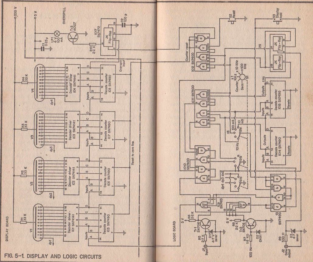
FIG. 5-1. DISPLAY AND LOGIC CIRCUITS
| Home | Audio mag. | Stereo Review mag. | High Fidelity mag. | AE/AA mag. |
The low cost unit to be described is simple in design and easy to construct. It makes a useful addition to the experimenter's workshop and an ideal introduction to more advanced digital systems.
Gas-filled cold-cathode indicator tubes are used for the four digit display which has switched decimal points and an "Overspill" lamp to warn when the maximum count of 9999 has been exceeded. A single five-way switch covers frequency in three ranges from 1 Hz to 1 MHz, pulse count unrelated to time from zero to 9999, and time in 0.1 second increments up to 999.9 seconds (16.6 minutes). A "Reset" button is fitted for manual reset to zero of the counter and time ranges, and a "Display-Hold" button enables the timer to be used as a stop watch. The input circuit will comfortably accept a wide range of input waveforms with amplitudes nominally from 2 to 20 volts, although circuit protection exceeds this value. A "Gate Output" socket is provided from which 10 mS, 100 mS, 1 S and 10 Hz pulses may be obtained depending on the range switch setting; thus, the unit may be used as a pulse generator for driving other digital circuits.
Accuracy is generally absolute on the "Counter" range, but is dependent on the timebase trigger frequency for other ranges.
In the basic form, the timebase is triggered from the 50 Hz mains supply, and although it is not unknown for the mains frequency to vary by as much as 2 Hz from the nominal 50 Hz (4% variation), this situation is fortunately rare. In practice, the variation is more likely to be within 1%. An alternative arrangement is to use the crystal controlled frequency reference shown in Figure 4-6, and space and power supplies are provided for this purpose. Accuracy can then better 0.1% ± one digit.
FIG. 5-1. DISPLAY AND LOGIC CIRCUITS
The Circuit
The display and logic circuits are shown in Figure 5-1. Starting from the input J l , the signal is applied via resistor R5 to the base of transistor TR1, which, with Zener diode D1 , isolates and protects the integrated circuits from excessive voltage. The transistor is followed by one of the Schmitt-trigger circuits contained in IC9. This "gates" the input, and produces pulses of precise amplitude and shape suitable for driving the counting circuits. A chain of four SN7490 decade-counters are used to cover units, tens, hundreds and thousands. These are connected by their 4-wire BCD outputs to SN74141 decoder-drivers which in turn drive the indicator tubes.
The indicator tubes are operated by maintaining a potential between anode and numeral-shaped cathode sufficient to ionize the gas and produce the characteristic cathode glow.
The anode is positive with respect to ground, so that the required numeral is illuminated simply by grounding, the appropriate cathode. Because the decimal points are a function of the range setting, they are controlled by range-switch wafer S1 a. The anode resistors are to limit the current through the tubes once the gas is ionized.
Before every pulse count, it is necessary to set all indicator tubes to zero. This is accomplished by making pin 3 of all four decade counters "hi" , although they must be "lo" during the counting process. Incidentally, the reset-to-nine function of the decade counters is made inoperative by earthing pin 7.
As each pulse arrives at pin 14 of the "units" decade-counter IC5, the number displayed by indicator-tube VI increases by one digit. At the tenth pulse the display reverts to zero, and the output at pin 11 goes from "hi" , where it had been since the eighth count, to "lo" ; thereby activating IC6 and changing V2 from zero to " 1" . The overall display now reads "0010" . As these operations are repeated, V2 increases by one digit for every ten input pulses until it passes nine and reverts to zero, when V3 reads " 1" . This goes on, with V3 increasing by one digit for every hundred input pulses, and V4 for every thousand until, finally, V4 passes nine and all tubes revert to zero.
Further pulses will produce an incorrect reading, because the counting chain is going round for the second time but lacks a " ten-thousand" digit. It is necessary, therefore, to warn the operator by lighting the "Overspill" lamp at the moment when all tubes revert to zero. Furthermore, the lamp must stay on until the counting chain is deliberately reset by the operator, or that he knows resetting has occurred. This is the job of Cl 7, which is reset with the decade-counters to make pin 8 "lo" until the count of ten-thousand, when it latches "hi" and activates the lamp driver TR3.
Frequency is measured by allowing the pulse count to take place for a precise period only. This period is defined by the width o f gate pulse applied to pins 1 and 2 of IC9. With a one-second pulse width, the readout is pulses-per-second or Hz. A full display reads 9999 Hz, or with the decimal point inserted, 9.999 kHz. The effective frequency range can be increased by reducing the gate width to 100 mS, because 9999 pulses in 0.1 seconds is equivalent to 99990 pulses in one second, or 99.99 kHz. Similarly, with a 10 mS gate, the full display reads 999.9 kHz.
Time is measured by applying a 10 Hz clock-pulse to the counter input also via pins 1 and 2 of IC9. This produces one count every 0.1 seconds, but with the decimal point in front of the first digit, the display actually reads seconds to the nearest tenth of a second.
Gate or clock pulses are derived from a special timebase circuit triggered by a 100 Hz signal, obtained either from the 50 Hz mains via the power unit, or from the crystal controlled frequency reference shown in Figure 4-6. The appropriate gate or clock pulse is selected by switch-wafer Sic and passed through the "Display-Hold" gate and inverter IC13 before being applied to pins 1 and 2 of IC9.
Provision is made to access the pulses via an isolating gate in IC13, protection network R9 D3, and output socket J2.
The shortest gate period required by the unit is 10 mS, which is equivalent to one half cycle o f a 50 Hz squarewave. To obtain a precise 1:1 mark-space ratio, however, it is necessary to start with a higher frequency and divide down. Hence the 100 Hz signal, which is processed by diode D2, transistor TR2, the second Schmitt-trigger in IC9, inverter. in IC13, decade- counters IC14 and IC15, and double flip-flop IC16, to provide all the intermediate frequencies and timing periods down to 0.25 Hz required by the unit.
When frequency is being measured, it is usually necessary to repeat the reading several times in order to detect drift or observe the result of some adjustment to the unit under test.
Control logic is derived from the timebase which, automatically resets the counter to zero, allows the count to occur, holds the display for two seconds so that the operator can read it, then repeats the operation. All this is achieved by combining different pulses from the timebase in the correct sequence and phase using the NAND gates IC10 and IC11.
Automatic reset is obtained by combining the 0.5 Hz and 0.25 Hz square waves in IC12 in such a way that a one-second reset pulse occurs every four seconds. Both "hi" and "lo" pulses are generated simultaneously in order to reset the decade-counters and overspill circuit. The manual "Reset" button operates by grounding pin 13 of IC12.
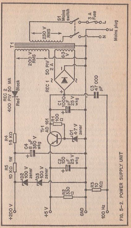
Fig. 5-2
The control logic previously discussed is set by range switch- wafer Sib. In the "Counter" and "Secs" positions, pin 5 of IC10 is grounded to keep pin 4 of IC9 "hi" , thereby admitting input and clock pulses. At the same time, automatic reset is inhibited by grounding pin 8 of IC16. As the range switch is moved through the frequency ranges from "XI" through to "X100" , more blanking waveforms are combined to produce a "window" in the four-second cycle sufficient for only one gate pulse. The "Display-Hold" button S3 operates by earthing pin 12 of IC13, and pin 9 of IC16, to stop pulse counting and automatic reset.
The power supply circuit is shown in Figure 5-2. Mains transformer T1 is a small instrument type designed mainly for valve circuits, but in this case the 6.3 V heater winding is connected to a full-wave rectifier D5 to provide the 5 Volt supply through a simple series regulator. The high voltage indicator tube supply consists o f a simple half-wave rectifier D3, with the smoothing and regulating network R3, R4, C2, and Zener diodes D1 and D2. The 100 Hz timing signal is derived from the unsmoothed output of the full-wave rectifier via C4 and R2. No pilot lamp is fitted because the indicator tubes light up immediately the unit is switched on. Mains protection is by the 2 ampere (or 3 ampere) fuse mounted in the 13 ampere mains plug.
Construction
The instrument is housed in a standard aluminum box measuring 8x6x3 inches. The display and logic circuits are mounted in the lid which becomes the front panel. The power supply components are mounted in the box so as to be well clear of the display and logic circuits when the front panel is fitted.
The power supply circuit diagram is shown in Figure 5-2, and the practical layout in Figure 5-3. It will be seen that the mains switch, mains transformer and power circuit board are mounted directly into the box with the latter spaced from the bottom of the box by two full 4BA nuts.
Plain unclad 0.15 inch matrix Veroboard measuring 5 x 2Vz inches is used, with Veropins inserted as necessary. A simple "U" shape heat sink made from 3 square inches of 18 gauge aluminum is mounted on the power board to accommodate the ADI 61 regulator transistor. It was found convenient to mount the high voltage rectifier on the transformer shroud, otherwise there is room in the bottom of the box between the circuit board and mains switch. Wiring is straightforward with the connections clearly shown in Figure 5-3.
If the crystal controlled frequency reference is to be used, it should be mounted on a circuit board not exceeding 2.5 x 4 inches, and inserted in the box at the place shown in Figure 5-3. The counter-timer will only require the 100 Hz output, ...
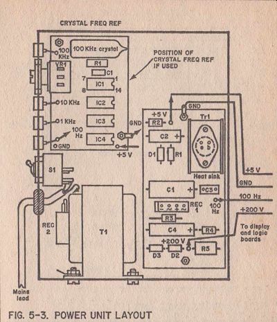
FIG. 5 -3 .
POWER UNIT LAYOUT
... but the higher frequency outputs can be made available via wander sockets let into the adjacent side o f the box, along with the frequency adjustment potentiometer which should be protected by a suitable cover or locking device.
The front panel layout, drilling template, and relative positions of the circuit boards and indicator tubes, are shown in Figure 5-4 and Figure 5-5. Once the panel is drilled, it may be covered with self-adhesive vinyl sheet. Next, the display window is "glazed" with red acetate sheet, cut 3/8 inch all round larger than the window to provide a gluing edge.
Finally, the switches, sockets and "Overspill" indicator lamp are fitted.
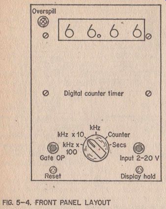
FIG. 5-4 . FRONT PANEL LAYOUT
Separate 0.1 inch matrix Veroboards measuring 5 x 2& inches are used for the display and logic boards. The method of mounting is shown in Figure 5-6, and it will be seen that the copper strips are uppermost when the front panel is laid face downwards. The components, including the ICs, are mounted on the insulated side before the boards are fitted to the front panel. This method leaves the stripped side accessible for wiring and testing. Before mounting the components, however, the copper strips must be interrupted at appropriate points to prevent unwanted connections (see Section 1). Also, holes are required to accommodate the fixing bolts and indicator tube connecting leads. Remember that these leads will have to be covered by plastic sleeving.
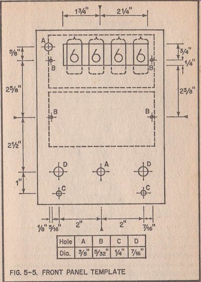
FIG. 5 - 5
The indicator tubes are secured to the display board by their leads and a simple wire twist around the top pinch. It is well to identify and mark the leads at this stage. The order of the connections is shown in Figure 5-7. Start by first identifying the lead to numeral "6" which is visible through the face of the tube. The IC pin numbers shown in Figure 5-7 are a mirror image o f those normally seen in data sheets because ...
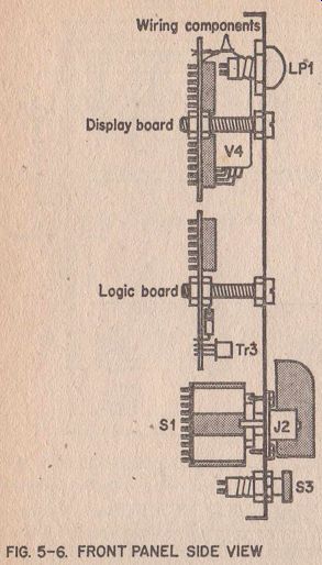
FIG. 5-6. FRONT PANEL SIDE VIEW
... the pins in this case are being viewed from below the device.
The other components are shown conventionally.
With all their components mounted and the connections clearly identified, the boards can be mounted to the front panel.
One inch 4BA bolts are used with spacer nuts arranged so that sufficient room is left between the boards and front panel to accommodate the indicator tubes. Note that the two center strips are at ground potential and coincide with the fixing nuts and bolts.
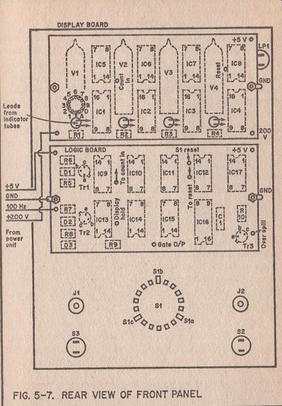
FIG. 5 -7 . REAR VIEW OF FRONT PANEL
It is impracticable to provide a full wiring diagram, but the information given in Figures 5-1 and 5-7 should be sufficient.
Interconnecting links are by single-strand plastic-covered tinned-copper wire. Unless Veropins are used, it is easier to solder the links direct to the component leads and pins rather than via the copper strips. Connections to the range switch are shown by Figure 5-7 in simplified form. If a multi-wafer switch is used, care should be taken to identify the correct switch tag. Finally, the power, ground and 100 Hz signal rails can be connected.
Once wiring is completed the unit may be tested. Switched to "SECS" , the display should change by one decimal digit every 0.1 seconds. The action of the "Reset" and "Display-Hold" buttons are best checked on this range. The "COUNTER" range may be checked by feeding in pulses from a suitable pulse generator, logic test set, or a simple DC supply such as a 3 volt battery. Finally, the frequency ranges can be checked against a reliable frequency source such as a crystal controlled oscillator.
Fault finding is not difficult provided it is approached in a logical fashion. After ensuring that the power supplies are correct, all other functions can be checked separately.
Remember that for NAND gates to open all inputs must be "hi" . For instance, if the counter function does not operate, it is possible that the potential on pins 1,2,4 of IC9 is "lo" . Try connecting the pins in turn to the 5 volt rail ("hi") to determine the incorrect circuit. By using this technique and a little patience, it is usually possible to locate incorrect connections or faulty components. Take care, however, not to introduce test signals greater than 5 volts DC or AC peak, other than through J1 .