AMAZON multi-meters discounts AMAZON oscilloscope discounts
LEARNING OBJECTIVES:
Upon completion of this Section on the print-and-etch technique for processing single-sided circuit boards, the student should be able to:
1. Apply photo-resist to copper foil.
2. Expose the photo-resist.
3. Develop the pc board and apply dye.
4. Prepare etchant solution and etch a pc board.
5. Use a wide-shank carbide-tip drill bit to drill the required holes in an etched pc board.
6. Strip and completely clean an etched board.
7. Process contact films for silk-screen printing.
8. Be familiar with the various available types of silk screens and printing inks and paints and select the appropriate type for a given application.
9. Prepare and use a silk screen for printing on pc boards.
0. INTRODUCTION
Of the many methods available for the processing of single-sided pc boards by the simple print-and-etch technique, the use of liquid photo-resist (wet film) is perhaps the most economically feasible for prototype work. This technique re quires inexpensive materials and equipment, thus making it ideally suited for this purpose.
The topics discussed in this Section include detailed discussions on circuit board cleaning, photosensitive resist application, etching, drilling, and the silk screen process for preparing marking masks.
In the wet-film technique of circuit board processing, certain methods are more suitable for prototype work, whereas others lend themselves more readily to mass production applications. The selection of a specific process will depend on such factors as costs, quantity of boards to be fabricated, and labeling and solder mask requirements. The use of the various chemicals and materials for processing are included to aid in the selection of the most appropriate method. Also included is information on simple construction of some of the equipment necessary for the various phases of board fabrication.
1. PHOTOSENSITIZING THE PRINTED CIRCUIT BOARD
For developing the conductor pattern onto the foil side of the copperclad pc board, a negative of the original conductor pattern artwork master is required. This negative becomes one of the basic elements used to process either one board for prototype work or hundreds of boards for mass-production requirements.
The surface of the foil must first be treated so that selected areas of the copper can be protected from the etching solution, which will remove all the copper except the conductor pattern. The copper may be treated by several methods to accomplish selective foil pattern protection. The method to be considered here is photosensitizing. In this process, the foil is treated with a photo-sensitive resist, exposed through a 1: 1 negative of the conducting pattern, arid developed. The result will be a 1: 1 positive conductor pattern produced onto the surface of the foil, which is etchant resistant, whereas the undesired areas of the foil are unprotected and will be removed by the etching process.
There are several chemicals readily available to implement this photosensitized technique. The chemicals and procedures discussed in this section are those of the Eastman Kodak Company. Chemicals of other manufacturers may require processing and exposure times that are different from those discussed.
The process begins by cutting the necessary-size copper-clad board from sheet stock. (See Section 10 for information on shearing pc boards.) The work must then be thoroughly cleaned before the photo-resist is applied. This cleaning is essential in order to remove all contaminants, such as grease or copper- oxide film, which readily forms on exposed copper. Unless these contaminants are removed, they will adversely effect the adhesion of the resist with the cop per surface.
The copper is first chemically cleaned in a 5 to 10% by volume bath of hydrochloric acid and water. This bath will remove copper oxide and grease film for the improvement of photo-resist adhesion. To prepare this bath, 75 milliliters of hydrochloric acid is slowly added to 925 milliliters of cold tap water in a container of Pyrex or acid-resistant plastic such as polyethylene or polypropylene. (Caution: Never add water to acid. This causes violent eruptions to occur.)
After the board is removed from the acid bath, the copper foil is then scrubbed with a 3M Scotch-Brite 96 pad while water-spray rinsing. This technique is shown in FIG. 1. Firm pressure should be applied with small overlap ping circular motions. If the recommended cleaning pad is not readily available, any gentle abrasive household cleanser that contains no bleach is acceptable. Coarse abrasives should not be used because they would deeply scratch the soft copper foil. Proper cleaning removes contaminants without causing surface imperfections in the foil. Cleaning is sufficient when water flushed over the surface of the copper “sheets” and no water “beads” remain. Remaining grease contaminants will appear as dry spots from which the water tends to pull away. To complete the cleaning process, the foil is thoroughly rinsed with water and swabbed with a lint-free cloth to remove any remaining cleaner deposits. Once the copper is completely cleaned, all surface moisture must be removed. This is accomplished by first patting dry with a paper towel. Since moisture severely affects resist adhesion a final drying operation is important. Total drying will be achieved if the board is placed in a forced-air oven for approximately 10 minutes at a temperature of 120°F (49°C). After the board is removed from the oven and allowed to cool to room temperature, the application of the photo- resist can begin. The board must be handled carefully because fingerprints will contaminate the copper. The cleaning and drying process appears time- consuming and tedious, but it is only through a thoroughly clean and dry surface that a quality printed circuit will result.
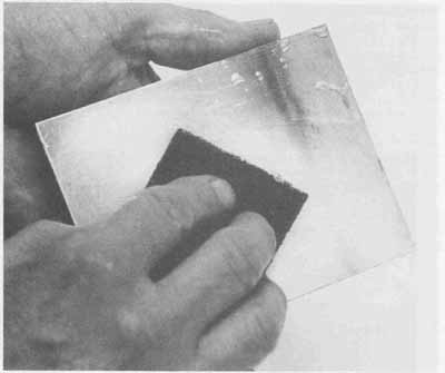
FIG. 1 Printed circuit board material contaminant removal is best accomplished
with a Scotch-Brite pad and cold water flush.
The application of liquid photo-resist is done by spraying, dipping, roller coating, low speed whirling, or flow coating. The first four methods are common to industrial applications and result in a consistently uniform layer of resist. These methods require expensive specialized equipment and, for this reason, are not intended for phototype pc board fabrication. Flow coating re quires no special equipment, and even though it does not produce a consistently uniform resist thickness, the results are acceptable.
Since the photo-resist is sensitive to ultraviolet light, safe-light conditions are required in its use. Lighting should be provided by red safe light (Wratten 1-A or equivalent) or fluorescent tubes covered with gold or amber plastic sleeves with the ends sealed with black vinyl electrical tape to prevent light leaks.
Kodak KPR liquid resist lends itself well to flow coating applications. This resist is clear in color and is applied directly to the pc board without thinning. For ease of application, a convenient amount of liquid resist may be transferred into a small bottle or other dispenser. FIG. 2 shows the application of Kodak resist with the use of a dropper. The resist is initially applied onto the center of the pc board. The board is then rotated and tilted in a circular motion so as to allow the resist to flow outward toward all four edges, thereby covering the entire surface of the copper. With this process completed, one corner of the board is tilted and placed into the mouth of the resist container to drain off all excess resist. The board is then placed in a horizontal position to dry at room temperature in a dust-free area. In approximately 10 minutes, the board is tack-free.
To ensure successful imaging with proper resist adhesion to the copper surface, a baking cycle is required. The baking removes any residual resist sol vent that may remain after being air-dried. Trapped solvent will prevent the conductor pattern image from being fully protected during the etching process.
Baking can be accomplished by either one of two methods. The first method is to place the board into an oven for 20 minutes at a temperature of 176°F (80°C) or a maximum of 10 minutes at 250°F (120°C). The second method is with the use of a 275-watt ruby-faced infrared heating lamp positioned 12 to 14 inches above the board. This process will require 20 to 30 minutes to eliminate resist solvent. In any type of baking cycle, extreme care must be exercised to avoid heat or light fog to affect the film. This would degrade the film and cause later processing problems. The resist surface temperature should not exceed 250°F (120°C). If using a lamp, reflectors should be opaque with no ultraviolet leaks.
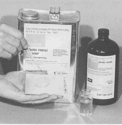
FIG. 2 Flow-coating a pc board.
After the photo-resist hardens in the baking cycle, it becomes sensitive to light. For this reason, care must be exercised to protect it from exposure to any intense light when removing the board from the oven or from under the lamp.
The board should be allowed to cool to room temperature prior to initiating the imaging process. Large-diameter 16-mm film cans provide a convenient means of storing sensitized boards for short periods of time.
Kodak KPR photo-resist can be exposed with a variety of sources rich in ultraviolet light, such as carbon-arc lamps, pulsed-xenon lamps, and unfiltered ultraviolet fluorescent lamps. In addition, a simple means of exposure is with a sun lamp used with an easily constructed exposure unit. This type of exposure unit is shown in FIG. 3a.
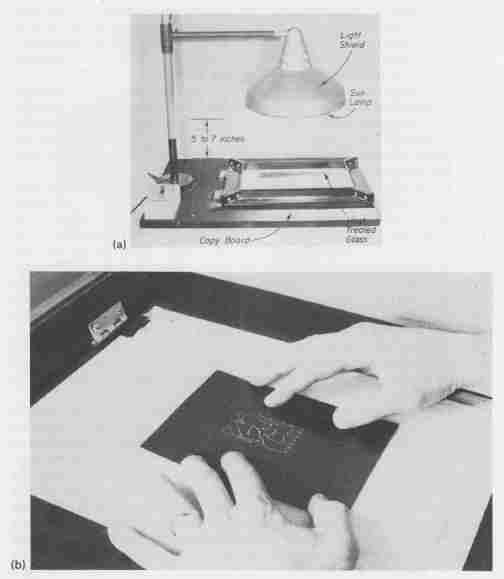
FIG. 3 Photo-resist exposure: (a) exposure unit; (b) correct alignment
of negative on sensitized copper.
Exposure time will depend upon such factors as light intensity, type of light source, distance of the source from the resist surface, and thickness of the resist layer. Optimum exposure can best be determined by trial and error. For the exposure unit shown in FIG. 3a, using a 275-watt sun lamp, optimum exposure results in 5 to 15 minutes with a lamp distance of 15 to 18 inches.
It is essential that the light source be provided with a shield that directs the light onto the work and at the same time protects the eyes from exposure to the light rays. Light in the ultraviolet range is extremely dangerous to the eyes and prolonged exposure must be avoided. If a light shield is not available, protective glasses should be worn. The pc board is placed onto the copyboard with the sensitized side up under safe-light conditions. The reduced negative of the conductor pattern is positioned directly onto the sensitized surface. It is held in direct contact with and flat against the pc board by the weight of the glass. The border delineation marks on the negative must be aligned with the corners of the board. In addition, the negative is positioned so that all literal and numerical designations are readable. Care must be exercised to ensure that the sensitized surface will be exposed through the correct side of the negative. If an orientation error is made and the board is later etched, it will be impossible to correct the conductor pattern. The correct orientation of the tone control circuit negative on the sensitized copper surface is shown in FIG. 3b.
Those photo-resist areas exposed to the light through the clear conductor pattern are polymerized and will become insoluble to the developer and thus remain on the copper. Those areas under the opaque portions of the negative are not exposed and remain soluble to the developer. This photo-resist will wash away, leaving a photo-resist mask on the surface of the copper that duplicates the desired positive conductor pattern.
The exposed board is developed with the use of a Pyrex or stainless steel tray that contains at least 1 inch of Kodak KPR developer. The board is placed into the tray with the imaged copper side facing up to prevent damage to the photosensitized emulsion. The amount of time that the board remains in the developer solution is critical. Normally, approximately 2 minutes at room temperature is sufficient to completely remove all of the resist areas that have not been polymerized by the light sources. The tray should be gently rocked for the full developing time. During the entire developing process, the remaining resist remains clear but a faint image of the conductor pattern becomes visible when the board is viewed at an angle under normal lighting conditions.
After the board is developed, it is removed from the tray, being handled only by the edges since the resist is soft and can be easily damaged. Both board surfaces are then flushed with cold tap water at high volume and low pressure for at least 30 seconds on each side.
The developed resist image is next inspected to determine if there are any imperfections, such as pinholes, bridges, or open paths. This inspection process makes use of Kodak KPR dye. The developed and rinsed board is dipped into a bath of this blue-colored dye for approximately 30 seconds. It is then removed and immediately flushed with cold tap water. This is shown in FIG. 4. The dye will adhere only to the photo-resist remaining after the developing process.
The board is next dried in an oven for 10 minutes at 250°F (120°C) or under a lamp at 6 to 8 inches for 10 minutes. In no case should the resist surface temperature exceed 250°F. After the drying cycle, the board is allowed to cool to room temperature.
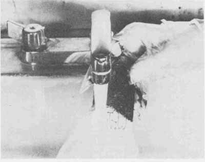
FIG. 4 Conductor pattern inspection is aided with the use of dye.
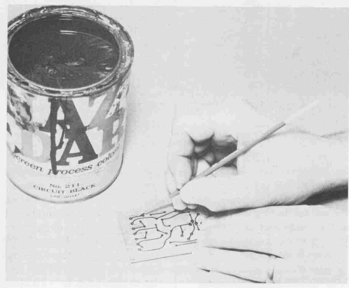
FIG. 5 Application of etchant resist to repair defective pattern.
The board can now be inspected and any errors or pattern imperfections that may be present can be corrected by using a sharp, pointed knife. If there are any breaks in the photo-resist covering of the desired conductor pattern at this point, they can be repaired by the application of etchant ink resist (non light-sensitive). This resist is carefully applied with a fine artist’s brush to close the break. It must overlap the photo-resist on either side of the break while maintaining width. This technique is shown in FIG. 5. There are a number of asphaltum-based materials available from graphic arts suppliers which may be used for this purpose. Some may require dilution to a workable consistency. The solvent used should be in the turpentine family. Solvents such as xylene or trichioroethylene should not be used since they tend to cause the resist to swell.
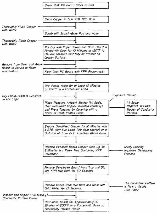
FIG. 6 Flow diagram for sensitizing printed circuit boards with photo-resist.
After the conductor pattern touch-up has been completed, another baking cycle is recommended to remove the solvent from the resist. A 20-minute cycle at approximately 200°F (93 °C) is sufficient to remove all solvents.
The photo-sensitizing procedure just discussed is an effective method of preparing a pc board for etching in prototype work. A flow diagram to aid the technician in following the many steps in this process is shown in FIG. 6. All the amplifier boards ready for etching are shown in FIG. 7.
FIG. 7 All pc etching boards for the amplifier processed and ready for etching.
2. CIRCUIT BOARD ETCHING
Etching is the process of attacking and removing the unprotected copper from the pc board to yield the desired conductor pattern. Several commercial etchants and techniques are available for processing pc boards. These materials and methods attack the unprotected copper yet do not affect the adhesive, supporting laminate, and photo-resist. The most common chemicals used by industry as an etchant are ferric chloride ammonium persulfate, chromic acid, and cupric chloride. Of these, ferric chloride is commonly used since it is less expensive and potentially the least dangerous.
Methods of etching include tray rocking, tank etching, and spray etching. Tray rocking is the simplest system, consisting of a tray of etchant attached to a powered rocking table. Tank etching involves dipping the work into a vat containing the etchant, which is maintained at an optimum temperature. Spray etching, although a much faster process, calls for etchant to be pumped under pressure onto the surface of the pc board. This method requires an elaborate and expensive system. These three methods will be described using ferric chloride as an etchant.
Ferric chloride (FeCl3) is an etchant that will react with the unprotected areas of the copper surface and produce copper ions, which are soluble in solution. This chemical is available premixed to the correct concentration. Ferric chloride crystals are also available if liquid storage is a problem but require premixing and concentration testing.
During the etching process, the concentration weakens because the soluble cupric and ferric ions precipitate out of solution in the form of a sludge that tends to settle on the bottom of the etching vat. When the etching time becomes excessively long, the used etchant should be discarded and replaced with a fresh solution.
Ideal etching conditions require that the etchant be heated to a temperature of between 100 and 130°F (38 to 54°C). Temperatures above this range should be avoided because of the fumes that are generated. Although etchant temperature is not critical, the activity of the etching process is increased when the solution is heated above room temperature. With the temperature maintained reasonably constant, the length of time required for etching will be consistent. However, because of the weakening of the solution, etching time will progressively increase.
In addition to heating, efficient etching requires that the etchant be continuously agitated to allow “fresh” solution to flow over the copper. A simple means of achieving this agitation is to use a Pyrex tray filled with etchant and placed on top of a rocker table. Rocking motion is imparted to the table by means of a small motor, cam, connecting arm, and off-center pivot arrangement. The pc board is placed copper side up in the tray. Only one board should be etched at one time since, because of the rocking motion, they tend to come in contact with each other. This could cause some of the etchant resist to be scraped off of a surface. As the table is rocked, a wave is generated in the etching solution that travels back and forth across the tray and board surface, keeping the major portion of any sludge formed off the copper surface. There are two disadvantages in using this arrangement. First, there is no method provided for heating the etchant unless an infrared heat lamp is used, in which case etchant temperature is difficult to control. Second, some sludge is continually carried over the surface of the board, which reduces some of the effectiveness of the etchant. However, outweighing these disadvantages is the fact that this system is relatively simple and inexpensive and suitable for prototype work. A 5- by 5-inch square of 1-ounce single- or double-sided pc board can be completely etched in approximately 30 minutes.
A more elaborate system for agitating the solution is shown in FIG. 8, consisting of a vat (Pyrex or other suitable nonmetallic material), heating tape, variable transformer, air feed, and thermometer. The temperature of the etch- ant contained in the vat is controlled by varying the voltage level delivered to the heating tape by the transformer. This temperature is monitored by a thermometer placed in the solution in proximity to the boards being etched. The etchant is circulated (agitated) by means of air pumped into the vat under low pressure and escaping through a perforated plastic tube placed along one side of the vat. The sludge (copper and ferric ions) settles to the bottom of the vat, allowing relatively sludge-free etchant to continually circulate across the surface of the work. The boards to be etched are suspended in the solution from noncorrosive rods and clamps with their copper side facing the source of the air bubbles. This method, although more expensive, can etch a 5- by 5-inch 1-ounce board in approximately 15 minutes.
Spray etching involves jet spraying the surface of the board with pressurized nozzles. Systems such as that shown in FIG. 9 also are available with a heating element to decrease etching time. With such a system, etching times of between 1 and 2 minutes can be realized without difficulty. The etching cycle is controlled by a mechanical timer. Several precautions should be pointed out. The thermostat setting should not exceed the manufacturer’s recommended maximum limits to avoid damage to the equipment. In addition, spray etchers of this type may be hazardous if the cover is not properly seated prior to operation to completely contain the etchant within the system.
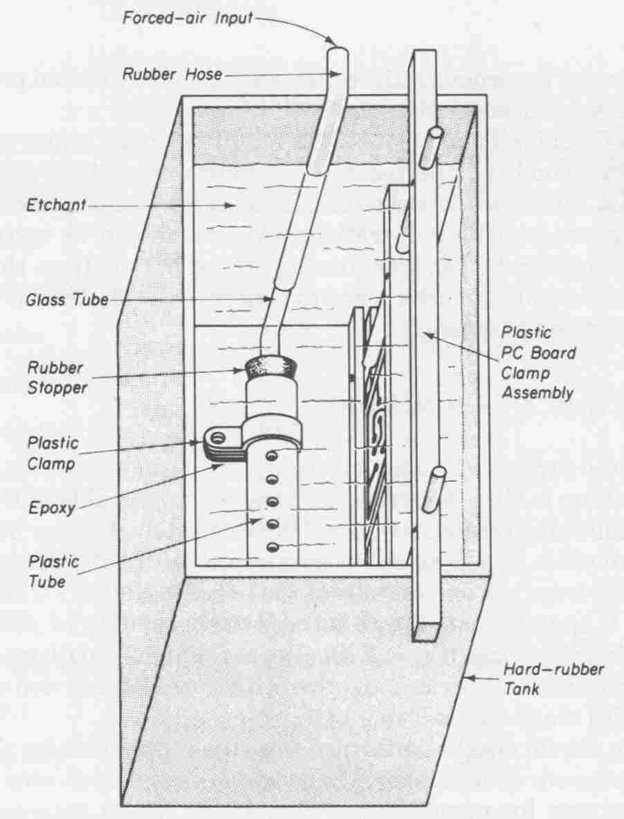
FIG. 8 Forced-air etching system.
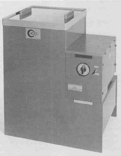
FIG. 9 Industrial etching system. Courtesy of Chemcut Corporation.
When the etching is completed, the board is rinsed under water for approximately 30 seconds and patted dry. This washing process will not remove the photo-resist, which is allowed to remain on the board to protect the copper during drilling and punching operations. Aprons should be worn to protect clothing and tongs used when transferring etched boards from the etchant to the initial rinse. After this washing and drying process, the boards are now pre pared for drilling and punching.
3. PRINTED CIRCUIT BOARD DRIUJNG AND PUNCHING
As was discussed in Sec. 6.2, a special wide-shank carbide tip bit is used to drill pc boards. Drilling is always performed from the copper side of the processed board for the following reasons: (1) to use the small etched center holes in terminal pads, which aid in bit alignment (it is extremely difficult to locate hole positions for drilling from the reverse side of the board, especially if the insulating base material is opaque), and (2) to minimize the possibility of pulling the cop per foil away from the base ( FIG. 10). The maximum lead diameter for some common components and devices together with the recommended drill sizes for lead access holes are shown in TABLE 1.
Punching should also be performed from the copper side for the same reasons just mentioned. If necessary, the grade of board used may require elevated temperatures for punching (see Sec. 10.2). Where necessary, an oven should be used for heating just prior to the punching operation. The punch and die should be sharp for best results. Before additional processing can be under taken, the board must be completely cleaned of all photo-resist, dye, and etch- ant impurities.
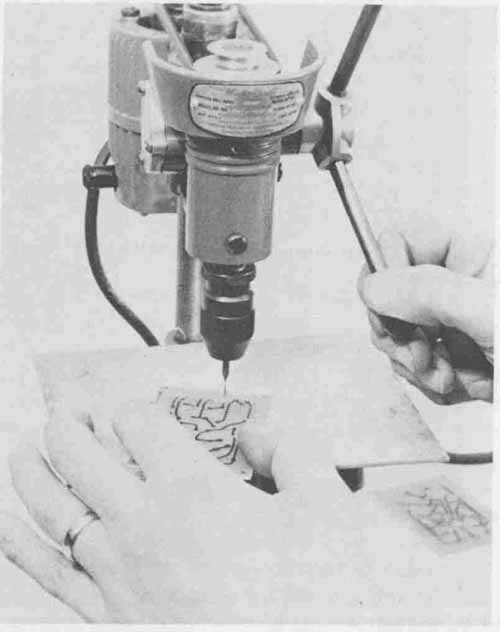
FIG. 10 Printed circuit board drilling with wide-shank carbide-tip
drill bit.
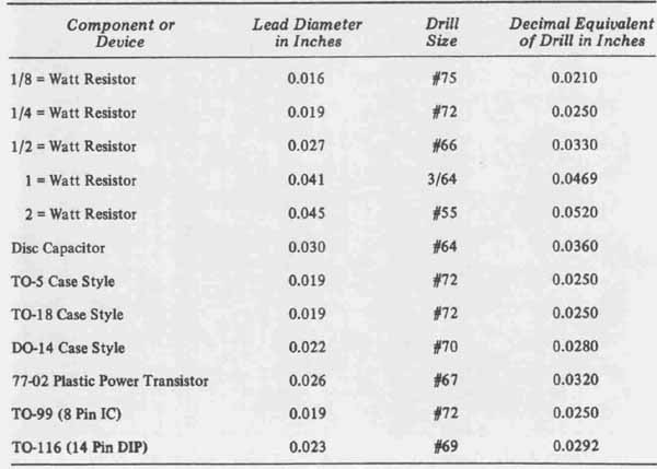
TABLE 1 Lead Hole Drilling Reference for Printed Circuits: Component
or Device; Lead Diameter
4. CONDUCTOR PATTERN SURFACE CLEANING
To prepare the etched copper surface for additional processes, the photo-resist and the dye are removed by dipping the board in a bath of Kepro PRSK photoresist strip It is then removed from the bath and scrubbed with a 3M 96 pad while water-spray rinsing. This scrubbing is essential to remove any photo-resist residue. If not removed, this residue can cause problems in soldering leads to terminal pads. The board is given a final water rinse for about 30 seconds.
Etching in a ferric chloride solution produces contaminants on the copper foil, which will adversely affect soldering or plating. These salts of ferric chloride require an additional cleaning process. The following procedure for their removal is recommended. The contaminating salts remaining on the copper are made water soluble by dipping and mildly agitating in a bath of Lonco Copperbrite No. 48 HT. A final water rinse for 1 minute will remove all residues from the copper surface. After this final rinse, the board is wiped dry with a lint-free cloth.
5. SILK-SCREEN PRINTING
A relatively inexpensive method of reproducing identical pc boards is by the silk-screen printing technique. This process utilizes ink resist that is applied through the stencil of the desired pattern that has been affixed to a fine-mesh silk screen. (Nylon or wire mesh can also be used.) Although the silk-screen method is extensively used for processing pc conductor patterns, the illustrative descriptions provided will involve preparing marking and solder masks. The end result will be stencils that will yield acceptable tolerances of line definition.
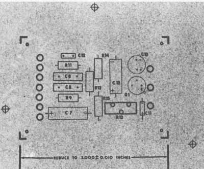
FIG. 11 Positive 1: 1 scale marking mask of tone control board.
The necessary materials to produce a silk-screen stencil are a silk or nylon screen mounted on a printing frame with hinged clamps, stencil film, film developer blackout, rubber squeegee, paint or solder resist, and the artwork master processed into a 1 1 scale positive or negative transparency. These materials and the procedures for producing and using a silk screen for the marking mask of the amplifier’s tone control circuit board will be discussed as an illustrative example.
The contact films used in the development of silk-screen stencils are normally extremely slow speed types with respect to exposure time and, as a result, do not require darkroom facilities. The film selected for this example is Ulano Super Prep. Even though the film speed is slow, it is recommended that this film be used in subdued light avoiding direct sunlight or high-output fluorescent lamps. The 1: 1 scale positive transparency, as shown in FIG. 11, is used to implement this film.
A piece of plain white paper, larger than the artwork, is first placed flat to serve as a background. The Super Prep film, allowing at least a 1-inch border on all sides, is placed on top of the white sheet with the sensitized (emulsion) side of the film positioned against the white paper. (The sensitized side of the film is determined by observing the dull finish as opposed to the glossy side of the polyester backing.) The initial arrangement of the film is shown in FIG. 12. The 1: 1 scale positive marking mask transparency is then placed on top of the film and held firmly in place with the glass printing frame. The film is then exposed with a 275-watt bulb, a No. 2 photo-flood lamp, or a Sylvania F20T12/BL ultraviolet lamp mounted at a distance of 15 to 18 inches above and directly over the film. The light source should not be closer than 15 inches from the frame to avoid excessive heating of the film. This is especially true when using photo-flood lamps. The exposure time for the film used in this example is approximately 10 minutes. Exposure times will vary from 5 to 15 minutes, de pending on such factors as film type, light source, and exposure distance. Optimum exposure times can be experimentally determined and once established, should not vary appreciably. Those areas of the film emulsion exposed to the light source will become insoluble in warm water after the developer bath. Those areas protected from the light by the opaque portions of the positive will dissolve in warm water after the developer bath. After exposure, the film is placed in a tray of developer with the emulsion side up for between 1 and 2 minutes. One end of the tray should be slowly raised and lowered to allow the solution to agitate gently over the surface of the film.
The developer for Ulano Super Prep film is available in powder form and packaged in premeasured packets labeled “A” and “B.” To prepare the developing solution, one packet of each of the powders is dissolved together in 16 ounces of water at a temperature of approximately 65 to 70°F (18 to 21°C). This developer is light sensitive and should be prepared in subdued light and stored in an amber-colored bottle. The solution has an effective lifetime of approximately 24 hours, after which time it begins to deteriorate. One indication of this deterioration is the appearance of wrinkles on the polyester support of the film during the developing process. When this occurs, the developer should be discarded and replaced with a fresh mixture.
After the film has been in the developer for the necessary amount of time, it is removed and immediately placed in a tray of water at a temperature of approximately 100°F (38° C). The emulsion side of the film is again facing up ward to prevent any smearing of the softened emulsion from the bottom of the tray. Gentle rocking of the water bath will remove the soluble portions of the emulsion (those areas protected during exposure). Approximately 1 minute is all the time required for the water bath to process the film. The film being processed in the water is shown in FIG. 13.
The film is next removed from the warm-water bath and rinsed with cold water for about 30 seconds to remove any remaining emulsion from those areas of the negative film that must be completely transparent. (Caution: Extreme care must be exercised when handling the film after it is taken from the warm-water bath since the remaining emulsion is soft and tacky and is easily smeared. The cold-water rinse is best applied by placing the film on a sheet of glass with the polyester support backing against the glass. The emulsion side can then be gently rinsed under a cold-water tap.)
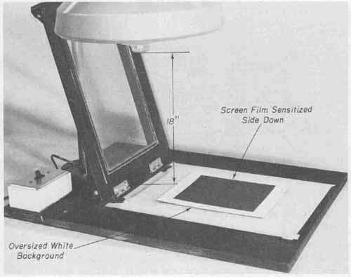
FIG. 12 Exposure arrangement for silk-screen film.
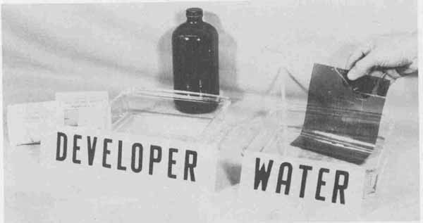
FIG. 13 Warm water used to process film after developing.
The silk-screen negative stencil of the original artwork master can now be obtained by firmly pressing the soft emulsion of the film against the surface of the silk screen. After the entire emulsion side has been pressed against the silk screen, both sides of the screen are gently blotted with soft absorbent paper towels to remove any excess water (FIG. 14). A block-out material, such as Ulano No. 60 Water Soluble Fill-in, is then spread with a small brush over the unused areas of the screen bounding the stencil. This block-out confines all excess paint or resist to the upper surface of the screen during printing ( FIG. 15).
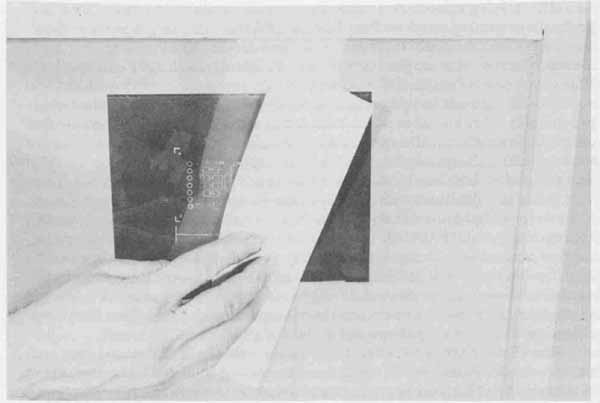
FIG. 14 Removing excess moisture from both sides of a silk screen.
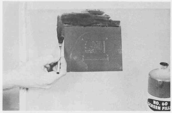
FIG. 15 Block-out applied to unused areas of screen.
The screen is then allowed to dry thoroughly. If a small fan is available, drying time will only require approximately 30 minutes. After the screen has dried, the transparent backing of the film is peeled from the screen, which is then carefully inspected by tilting it back and forth while holding it up to an intense light. No residual film should remain on those areas of the screen that are not blocked and appear as translucent. This residual film will appear to glisten and, if not removed, will impair smooth transfer of the paint or resist through the screen stencil during its application. This film is removed with standard mineral-oil spirits and a stiff brush. The emulsions forming the stencil or the block-out are resistant to these solvents and will not be affected by this cleaning process. The use of water, however, should be avoided because these emulsions are water soluble.
The stencil just developed is now ready for use. Before proceeding, how ever, some consideration needs to be given to the type of screen to select for a particular application. In this section, the concern centers around screens for marking and solder masks. Therefore, a moderate degree of control must be maintained on positioning paint or resist flow through the screen in order to effect acceptable line definition.
Screens are classified in two categories, mesh number and durability. Mesh numbers for silk screens, generally running from No. 1 to No. 25, refer to the number of filaments per inch. A No. 1 mesh screen has approximately 30 filaments per inch and is considered very coarse. Mesh No. 25 represents a fine screen of approximately 196 filaments per inch. The more the filaments per inch, the greater the control of paint or resist flow through the screen and consequently the sharper the resulting pattern. For extremely critical line definition, mono filament nylon mesh screens with as many as 283 filaments per inch are also available. For applying epoxy paint for marking masks and solder resist for solder masks, a screen with a mesh number of 20 will produce adequate results. This mesh is also suitable for conductor pattern stencils.
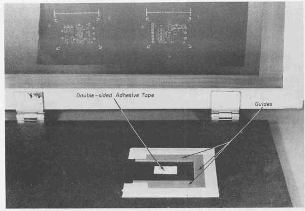
FIG. 16 Register guides to aid in board alignment.
The durability of the screen is a measure of its ability to withstand continued reuse. Durability classifications are X, XX, and XXX, with the latter used only if many reproductions are to be made. For prototype work, screens with a durability classification of X are adequate. However, if the screen is to be continually stripped clean and reprocessed for other stencils, XX, XXX, or wire mesh screens should be considered.
To facilitate the silk-screen labeling process, it is first necessary to provide a base and a set of clamp hinges to accommodate the frame and also to provide positive positioning of the surface to be labeled. These aids are shown in FIG. 16. The frame is clamped to the printing base by means of the clamp hinges in such a manner that the stencil is closest to the base as the frame is swung down into the printing position. With the frame properly clamped, the pc board is placed on the printing base under the frame and its corners are aligned with the border delineation marks on the stencil. Once the desired alignment is achieved, three small register guides cut from either cardboard or metal, no thicker than the board, are positioned against any three board edges. This procedure is also shown in FIG. 16. The register guides are secured in place with masking tape and help hold the work in position during printing. They also allow for rapid positioning of identical workpieces when many boards are to be processed.
Once the work and stencil are properly aligned, a liberal amount of epoxy- type paint is poured across the left-hand margin of the marking mask stencil from top to bottom. A hard-rubber squeegee, preferably one that will span the entire stencil, is brought down onto the screen behind the pool of paint. With a sweeping motion, the squeegee is drawn across the stencil, spreading the paint as it moves. This technique is shown in FIG. 17a. Familiarity with this technique will enable the technician to completely label the entire work surface with a single sweeping motion.
After the stenciling is completed, the screen is raised from the work ( FIG. 1 7b). Small boards may tend to cling to the stencil when it is raised. Usually, they will slide slightly before they fall, thus causing the labeling to smear. This problem can be avoided by using double-sided adhesive tape placed on the underside of the work when it is first positioned on the base.
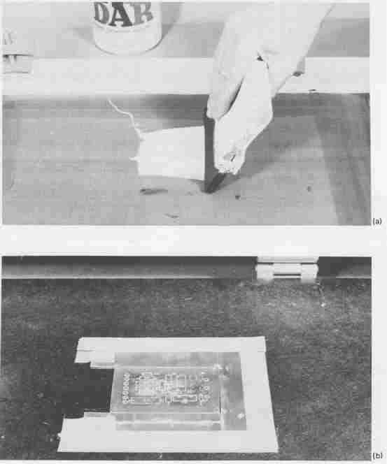
FIG. 17 Use of silk screen for board marking: (a) a single stroke of
the squeegee labels the board; (b) results of the screening process.
When labeling has been completed, the paint must be allowed to dry thoroughly before handling. Depending on the type of paint used, drying time will vary from 2 hours to a complete curing time of 4 days. Drying time can be reduced by baking according to paint manufacturers’ specifications. Certain lacquers and vinyls used in the silk-screen process for labeling will air dry in 5 to 15 minutes. No difficulty will be encountered in obtaining any desired labeling characteristics in terms of color, durability, or finish because there are hundreds of different types of paints, enamels, and lacquers available from graphical suppliers. A list of some printing inks used for silk-screen printing is given in Appendix IV. The seven labeled pc board of the amplifier together with the stencils used for each are shown in FIG.
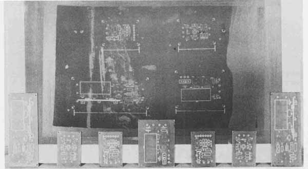
FIG. 18 Marking mask with all boards screened.
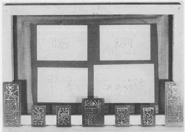
FIG. 19 Solder mask with all boards screened.
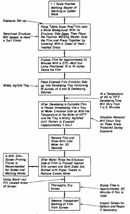
FIG. 20 Flow diagram for developing silk-screen stencils.
When the labeling process has been completed, the excess paint can be removed from the margins of the stencil with a small spatula and stored. The remaining paint is then washed off with an appropriate solvent. If the existing stencil is no longer to be used, the screen can be reclaimed for further stencil use by washing it in warm water. This will dissolve the water-soluble emulsion and blockout. Difficult areas can be gently scrubbed with a soft-bristle brush.
The discussions above have been limited to silk-screen printing for producing marking masks. This process is also used for processing solder masks. For this purpose, the procedures for developing the stencil are identical except that a 1: 1 negative is used initially to generate the silk-screen film. Also, in stead of using an epoxy paint, a solder resist, such as Lambert No. 184-10-V green solder resist, is applied through the screen.
The silk-screen stencils and finished boards with solder masks applied to the amplifier’s pc boards are shown in FIG. Because of the complexity of the silk-screen process, a flow diagram is provided in FIG. 20 to help the technician follow the various steps.
After the pc boards have been processed, the components and hardware must be mounted and leads soldered securely to the conductor pattern. The procedures and equipment necessary for this phase of construction will be discussed in the succeeding Sections.
EXERCISES
A. Questions
1 What is the purpose of photo-resist?
2 How should pc board copper surfaces be cleaned prior to the application of photo-resist?
3 List the various methods of applying photo-resist.
4 Define the term etching.
5 What would be the result if a positive phototool was used to contact print the photosensitized board instead of a negative phototool?
6 What is the correct orientation for the negative when contact printing the photosensitized board?
7 Define the term polymerize.
8 What precaution must be observed when developing exposed photoresist?
9 After the application of liquid photo-resist, why are the pc boards dried in an oven?
10 Determine the required drill sizes for watt resistors, disc capacitors, and DO-14 case leads. Which component requires the largest hole size?
B. True or False
Circle T if the statement is true, or F if any part of the statement is false.
1 Etching efficiency increases with agitation and decreased temperature. T F
2 Before drilling a pc board, each terminal pad is center punched. T F
3 The flow coating of photo-resist requires no special equipment. T F
4 Ferric chloride is commonly used as an etchant. T F
5 Drilling of a pc board is performed from the opposite side of the copper conductor pattern. T F
6 The contact films used in the development of silk-screen stencils do not require that they be used under safe-light conditions. T F
7 Some grades of pc board require elevated temperatures prior to punching. T F
8 Etchant resist is removed by scrubbing the board with a Scotch-Brite Pad. T F
9 Developer solution for Ulano Super Prep film is light-sensitive. T F
10 A silk screen with a mesh number of 2 is ideally suited for conductor pattern stencils. T F
C. Multiple Choice
Circle the correct answer for each statement.
1 Light-sensitive photo-resist is exposed with a (black, infrared) light.
2 When preparing a bath of hydrochloric acid cleaner the (water, acid) is slowly added to the (water, acid).
3 The drilling of a processed pc board is performed from the (insulation, copper) side.
4 Kodak KPR liquid resist is (clear, amber) in color.
5 To expose photo-resist, the negative is positioned so that literal and numerical designations are (forward-, reverse-) reading.
6 An exposed board to be developed is placed into the developing tray with the imaged copper side facing (up, down).
7 After the touch-up process has been completed, the board is baked to remove (gases, solvents) from the resist.
D. Matching Columns
Match each item in column A to the most appropriate item in Column B.
COLUMN A 1. Copperbrite 2. Sun lamp 3. Water “sheeting” 4. Etchant 5. Photo-resist developing 6. Silk-screening 7. Mesh number |
COLUMN B a. Clean copper foil b. Rubber squeegee c. 2 minutes d. Contamination remover e. 3600 angstroms f. 30 filaments/inch g. Ferric chloride |
PROBLEMS
1 Fabricate printed circuit device test jigs from the artwork masters de signed in Problem 11.2 using h-inch-thick FR-4 board with 1-ounce cop per foil. The final etched boards are to be drilled with the appropriate size holes to accommodate suitable turret-type terminals for external inter connections and socket pins for the devices. The terminals and pins are installed in Problem 14.2.
2 Prepare silk screens for the marking and solder mask layouts designed for the tachometer circuit of Problem 11.5. (The screens are used in Problem 13.6.) Obtain the meter movement specified for the circuit. Using a commercially available tachometer as a calibration reference, redesign the meter scale and construct a silk screen for the new scale.
3 Fabricate a pc board from the artwork master of the seven-fixed-interval UJT timing circuit designed in Problem 11.3 from 1/16-inch FR-4 board with 1-ounce copper foil. Components are assembled in Problem 14.3.
4 Construct a pc board from the artwork master for the series feedback regulator circuit designed in Problem 11.4 from 1/16-inch FR-4 board with 1-ounce copper foil. Components are assembled and soldered in Problems 14.4 and 15.4, respectively.
5 Fabricate a pc board from the artwork master for the tachometer circuit designed in Problem 11.5 from -inch XXXP board with 1-ounce copper foil. Using the silk screens fabricated in Problem 13.3, construct the meter scale, mark the pc board, and mask the conductor pattern for soldering. Components are assembled to the pc board in Problem 14.5.