Integrated circuits are finding increased application in commercial a-m, fm, and TV receivers and somewhat less lively adoption for small transmitters. At this writing, the IC is also attracting the attention of hobbyists and experimenters who build their own communications equipment. It seems reasonable, therefore, to expect that the IC eventually will bring about marked simplification of communications circuits--in the RF and video, as well as audio, sections.
This section describes the application of !Cs to several familiar receiver and transmitter functions. Other uses of a similar nature will suggest themselves to the reader.
For other setups (other than audio amplifiers) that also are suitable for use in communications equipment, see Sections 2.13, 2.14, 2.15, 2.16, 3.5, 3.6, 3.7, 4.2, 4.3, 4.4, and 4.5.
The reader will note that many of the setups described else where in this guide may be combined in various ways to provide various receiver and transmitter functions, just as larger-sized modules similarly may be combined.
1. SIMPLE RADIO RECEIVER
Fig. 1 shows the connections for a simple tuned-diode type of a-m radio receiver. In this rudimentary arrangement, the signal is tuned in by the L1-C1 tank, in which L1 is a tapped, ferrite loopstick antenna. The tap affords a good impedance match to the low-impedance diode X1, which may be any general-purpose germanium unit. The signal is DC modulated by X1, and the resulting AF output is amplified by the IC that drives the speaker. This setup is very effective for reception of local a-m stations in the standard broadcast band, and may be used at higher frequencies if a suitable inductor and outside antenna are substituted for L1.
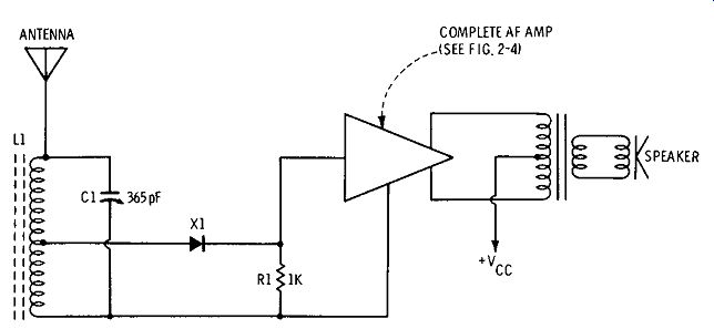
Fig. 1. Simple radio receiver.
The modulation component of the signal is amplified by the IC, which combines both preamplifier and power output amplifier functions. A suitable IC is the Type CA3020 that is described in Section 2.5, Section 2. Operated from a single 9-volt DC source, this IC delivers ½ watt to the loudspeaker.
A 35-m V detector output signal drives the amplifier to this full output. The entire amplifier should be used, as shown in Fig. 4, Section 2.
The sensitivity of a receiver circuit of this type is entirely a function of the gain of the audio amplifier, since the RF portion of the circuit is merely a diode detector and provides no amplification. With the CA3020 IC, the minimum RF signal amplitude for full speaker volume is somewhat in excess of 35 mV. If additional sensitivity is desired, a high-gain AF preamplifier may be operated between the diode detector and the input of the audio amplifier, or an RF preamplifier may be operated ahead of the detector--or both may be used.
Suitable amplifiers of both types are described in Section 2.
It should be borne in mind when using only high-gain audio amplification, however, that the minimum RF signal amplitude at which the diode will operate properly is approximately 0.5 mV. A simple receiver of this type has a number of applications, including compact and small-sized provision for broad cast reception, special signal monitoring, and personal paging pickup. In control applications, an electronic relay circuit may be operated in place of the speaker.
2. IC SUPERHET RECEIVER
ICs, together with any required outboard components, may be combined in a number of ways to provide complete receiver operation at a more sophisticated level than that of the simple receiver described above in Section 1. Fig. 2 shows the functional layout of an a-m superhet receiver.
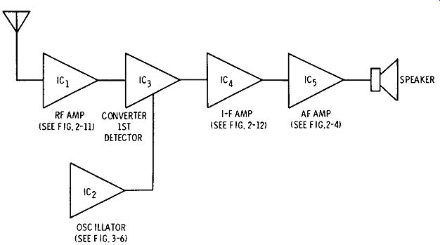
Fig. 2. Layout of superhet radio receiver.
In this arrangement, IC1 is an RF or wideband amplifier with external tuning, IC2 is a wideband amplifier adapted for self-excited oscillation and for gang-tuning with IC11 and ICa (the converter stage) may be a suitable diode mixer or it may be a transistor circuit supplied by a transistor-array IC. IC4 is an i-f amplifier with external transformer coupling, and IC5 comprises the second detector and audio stages. Suitable selections and arrangements of ICs for these various stages are discussed in Sections 2 and 3. In some arrangements, two RF and two i-f stages will be employed; and in some, an IC containing a second detector and an AF preamplifier will precede the audio output stage.
In general, the adapting of a superhet receiver to ICs presents little difficulty, but the process contributes a great deal to simplification and miniaturization of the receiver.
Most external components intended for use with transistors (tuning inductors, i-f transformers, miniature audio trans formers, etc.) are compatible with ICs.
3. UNTUNED RF AMPLIFIER FOR RECEIVERS
An untuned RF preamplifier is very effective in boosting weak signals before they reach the input of a receiver, and also for improving the signal-to-noise ratio of the receiver.
A wideband IC amplifier, such as a video-amplifier type, will perform this function without tuned circuits, and the tiny IC (with its few outboard components) may be tucked into even the smallest receiver.
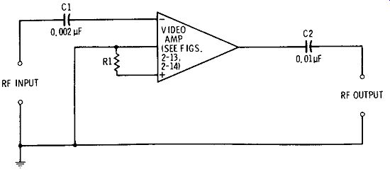
Fig. 3. Untuned RF preamplifier for receivers.
Fig. 3 shows the simple arrangement for such a pre amplifier /booster. This arrangement requires only two external capacitors and one external resistor, in addition to the video-amplifier IC (e. g., Type CA3001). Similar video amplifier arrangements are shown in Figs. 13 and 14, Section 2, and described in Section 2.16.
The user should select the video amplifier IC that gives the highest gain at the frequency at which he will most often use the receiver. In approximately the lower half of the IC frequency response, however, the gain is fairly flat over a considerable frequency band. The Type CA3001 IC, for example, provides a voltage gain of 18 dB, flat within 1 dB from DC to 6 MHz, a span including the standard broadcast band and all of the assorted services from the top of that band to 6 MHz.
4. IC FM RECEIVER STAGES
Fig. 4 shows the internal circuit of the Type CA3013 IC, designed to supply the i-f amplifier, discriminator, and AF amplifier stages of an fm superhet receiver. Considerable compactness and simplification are afforded by this small IC, which is housed in a 10-lead TO-5 can. This unit has a useful range extending from 100 kHz to higher than 20 MHz. Used in place of the i-f, second detector, and AF sections shown in Fig. 2, this IC would convert the latter circuit from a-m to an fm receiver. Fig. 5 shows how the same IC supplies the sound i-f and the detector channel of a TV receiver.
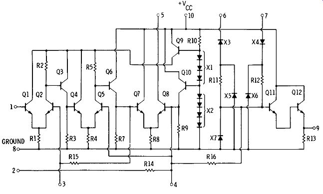
Fig. 4. IC for fm i-f amplifier/discriminator/AF amplifier.
The CA3013 (Fig. 4) contains three direct-coupled amplifier-limiter stages in cascade ( Q1 to Q8), a DC supply voltage regulator ( diode groups Dl and D2 and transistors Q9 and Q10), discriminator diodes (D3 and D4), signal-filter diodes (D5, D6, and D7), and a Darlington-pair AF pre amplifier (Q11 and Q12). An external discriminator transformer is connected to terminals 4, 5, 6, 7, and 10 (see also Fig. 5). The input i-f transformer is connected to terminals 1 and 2.
The small IC, the size of a small-signal transistor, reduces the external complication of this multistage fm circuit by several orders of magnitude.
5. IC TV SOUND 1-F AMPLIFIER AND DETECTOR
The fro-channel IC described in Section 5.4 is shown functioning as the sound i-f amplifier and detector channel in an intercarrier TV receiver in Fig. 5. The description of the CA3013 given in Section 4 applies here also.
The TV sound channel, exclusive of the audio output amplifier, is reduced to a transistor-sized IC and nine outboard components: i-f transformer T1, discriminator transformer T2, capacitors C1 to C6, and resistor R1. The arrangement is adapted from the original RCA design.
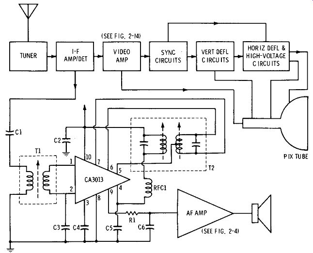
Fig. 5. IC TV sound i-f amplifier and detector. (After RCA.)
6. PRODUCT DETECTOR
In transmission systems involving carrier suppression and retention of one or more of the sidebands, the carrier must be reinserted at the receiver. This may be accomplished in a product detector. The same method is used in some specialized test instruments.
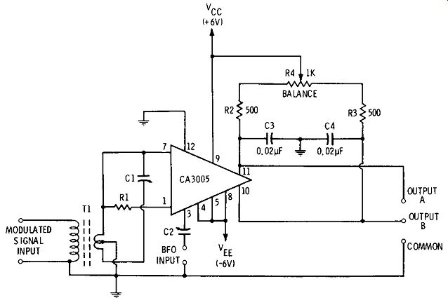
Fig. 6. Product detector.
Fig. 6 shows a product-detector circuit adapted from the original RCA design for the Type CA3005 IC. This IC is basically an RF-amplifier type consisting of two matched, common-emitter amplifiers whose emitter circuits are common to both. The useful frequency range extends from O to 100 MHz. In this detector circuit, the modulated signal is applied to IC terminals 1 and 7 (the bases of the two signal transistors) in push-pull, and the missing carrier is supplied by an external carrier oscillator (BFO) to terminal 3 (essentially to the emitters of both transistors in parallel). Variable capacitor C1 must be selected to tune the input transformer (T1) to the frequency of the modulated signal, and C2 is selected for critical adjustment of the supplied carrier amplitude. The balanced nature of the differential pair of transistors contained in this IC makes it comparatively easy to obtain balanced-circuit operation, provided the secondary winding of transformer T1 is accurately center tapped. Symmetrical output is provided by terminals 10 and 11 (the collectors of the signal transistors). As is seen from Fig. 6, very few outboard components are required. Aside from the input transformer (T1) and coupling capacitor (C2) and tuning capacitor (C1), already mentioned, there are only the collector load resistors (R2, R3) and collector capacitors (C3, C4), all four being matched components.
7. BALANCED MODULATOR
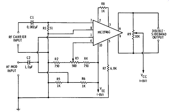
Fig. 7. Balanced modulator.
Communications techniques involving carrier suppression and sideband selection (as well as certain test instruments, such as heterodyne wave analyzers) employ balanced modulators for suppression of the carrier and transmission of the sidebands. The differential IC amplifier offers marked virtues as a balanced modulator: close symmetry due to excellent matching of the integrated components, a compact modular unit requiring the minimum of external components, and easily balanced input and output.
Fig. 7 shows the connections for a balanced modulator employing a Type MC1596G IC. In this arrangement, potentiometer R3 is the offset adjustment, and potentiometer R9 is the output-balance adjustment. Adjustment of these two potentiometers causes the carrier to be rejected by better than 60 dB. As in all conventional triode-type balanced modulators, the carrier is applied to the two halves of the input circuit out of phase, while the modulation is applied to the inputs in parallel.
The modulator delivers double-sideband output, but a single sideband may be selected by means of a sharply tuned bandpass filter and amplifier. The balanced modulator is useful also in chopper applications and in phase detection.
8. MISCELLANEOUS RECEIVER AND TRANSMITTER APPLICATIONS
Various IC setups described elsewhere in this guide are useful in receivers and transmitters, in addition to the specific applications for which they were discussed. The audio amplifiers described in Sections 2.2, 2.3, 2.4, and 2.5, for example, may be employed in the audio/speech/modulator channel of a transmitter. Selective cw reception may be obtained by inserting a bandpass amplifier (Sections 2.6 and 2.7) into the AF channel of a receiver to pass the desired signal, or a bandstop amplifier (Sections 2.8 and 2.9) into the AF channel to remove an undesired signal. The RF, i-f, and video amplifiers described in Sections 2.13 to 2.16 may be used directly in receivers.
The AF oscillators described in Sections 3.1 to 3.4 may be used for tone modulation of a transmitter. The combination oscillator (Section 3.6) can function as a variable-frequency oscillator in a transmitter when followed with a suitable buffer amplifier for boosting its low output power. The crystal oscillator, when similarly followed by a suitable RF power amplifier/buffer, may be used as the oscillator section of a transmitter.
The sensitive AF/RF relay described in Section 4.2 may be used to switch a receiver off when the transmitter goes on the air. And the threshold circuit may be used as an overmodulation alarm in a-m stations. (If the rectified carrier voltage is applied to one input, and the rectified modulation voltage is applied to the other input, and the ratio of the two applied voltages is correctly adjusted, the threshold circuit will deliver an output signal whenever the predetermined modulation percentage is exceeded.) The self-excited RF oscillator may be used as the high-frequency oscillator in a superhet receiver and may also be used as the cw oscillator (beat-frequency oscillator) in a receiver.