AMAZON multi-meters discounts AMAZON oscilloscope discounts
4. SENSITIVITY ANALYSIS
The sensitivity analysis constitutes the bulk of the design. The routing study is used to determine the layout solution space. The sensitivity analysis is used to determine the electrical solution space. The area where both of these solutions spaces overlap constitutes the design solution space. The sensitivity analysis will rank the variables as to how strongly they affect the system and highlight which variables affect the solution most and in what way they affect the system. This allows the designer to get a hold of a problem with a great number of variables.
During a sensitivity analysis, every variable in the system bus is varied in simulation. The performance metrics, such as flight time, flight-time skew, and signal integrity, are observed while each variable is swept. The performance as a function of each variable is compared to the timing and signal quality specifications. The result is a solution space that will place strict limits on the system variables under control of the designer (such as trace lengths, spacing, impedance, etc.). The solution space will lead to design guidelines for the PCB, package, connectors, termination, and I/O.
4.1. Initial Trend and Significance Analysis
An initial Monte Carlo (IMC) analysis can be used to determine the significance and trend of each variable in the system. This is necessary for two reasons: First, the trends will point to the worst- and best-case conditions. This will allow the engineer to define the simulations at the worst- and best-case corners. In a design with a large number of variables, it is almost impossible to pick the worst-case conditions by reasoning alone. The IMC analysis will point directly to the corner conditions. Second, the IMC can be used to determine which variables most affect performance. Subsequently, significant time can be saved by prioritizing the analysis and concentrating primarily on the most significant variables. After a rough topology and all the system variables have been estimated, a Monte Carlo analysis should be performed. Every single variable in the system should be varied with uniform distribution over a reasonable range that approximates the manufacturing variations.
It is not necessary to perform more than 1000 iterations because the analysis is not meant to be exhaustive. After the IMC is performed, each variable is plotted versus a performance metric such as flight time, skew, or ringback. A linear curve is then fit to the data so that the trend and correlation can be observed. A linear relationship is usually adequate because all the input variables at this stage should be linear. Furthermore, since these variables are being swept, it is usually optimal to use linear buffers. So, basically, what is that done is that a great number of variables are allowed to vary randomly ( Monte Carlo), and the results for several defined timing and signal integrity metrics are recorded (usually automatically from scripts written to filter the output or utilities contained in the simulation software). The observed metrics can then be plotted versus system variables. If the metric is strongly dependent on the system variable, it will "stand out" of the blur and be easily recognizable.
FIG. 16 depicts a conceptual IMC output. The plot depicts the flight time from a Monte Carlo analysis (with several variables) plotted versus only one variable, the receiver capacitance. A best linear fit was performed on the data and the correlation factor was calculated using Microsoft Excel. The correlation factor is a measure of how well the linear approximation represents the data. A value of 1.0 indicates that the linear approximation is a perfect representation of the data. A value of 0.0 indicates that no correlation exists between the linear approximation and the data. In an IMC analysis, the correlation factor can be used to determine how dependent the overall metric is on the particular variable being plotted (in this case the flight time versus capacitance). If the correlation factor is high, the metric is highly dependent on the variable. If the metric has no linear trend when plotted against the variable, the correlation factor will be very small. In the case of FIG. 16, since the correlation factor is 0.96, out of all the parameters varied in the Monte Carlo analysis, the flight time is almost exclusively dependent on the I/O capacitance. The slope of the linear fit indicates the trend of the variable versus the metric. The positive slope indicates that the worst-case flight time will be achieved with large capacitance values. Furthermore, if it is difficult to obtain the correlation factor, the magnitude of the slope provides insight into the significance of the variable. If the slope is flat, it indicates that the variable has minimal influence on the metric. If the slope is large, the variable has a significant influence on the variable. In large complex systems, this data is invaluable because it is sometimes almost impossible to determine the worst-case combinations of the variables for timings and signal integrity without this kind of analysis.
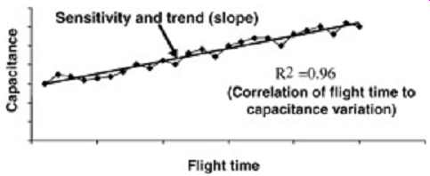
FIG. 16: Receiver capacitance versus flight time: IMC analysis that shows
maximum receiver capacitance produces the longest flight time.
It should be noted that sometimes a small number of variables will dominate a performance metric. For example, length and dielectric constant will dominate flight times. When these variables are included in a large IMC analysis, the correlation factors associated with them will be very high and all the others will be very low. Subsequently, all the trend and significance data associated with the other variables will be pushed into the noise of the simulation. Usually, after the initial IMC analysis, it is necessary to limit the variables for subsequent runs by fixing the dominant variables. This will pull the significance and trend data out of the noise for the less dominant variables.
FIG. 16 was an ideal case. For a more realistic example, refer to FIG. 17. A Monte Carlo analysis was performed on a three-load system and every variable in the system was varied randomly with a uniform distribution over reasonable manufacturing tolerances (19 variables in this case). FIG. 17 is a scatter plot of the delays produced during a 1000 iteration Monte Carlo analysis plotted against the impedance of the motherboard, the daughtercard trace, and the package trace. The best linear fit was performed on each data set. Both the trends and the significance are determined by the results of the linear approximation. Since the slope of the line is positive for the PCB impedance, the delay of the nets will increase as the trace impedance increases. Furthermore, since the slopes of the package and daughtercard impedance are negative, this means that the longest delay for this particular system will be achieved when the PCB impedance is high and the package and daughtercard impedance are low. This result is definitely not intuitive; however, it can be verified with separate simulations. Additionally, the correlation factor is used to determine the significance of the variables. Since the correlation factor of the PCB impedance is the highest, it has more influence on the signal delay than does the daughtercard or package impedance.
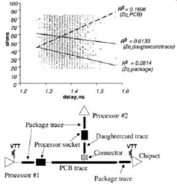
FIG. 17: Using IMC analysis to determine impedance significance and trends.
FIG. 18 is a plot of the same Monte Carlo results as those shown in FIG. 17 plotted versus the I/O capacitance and the socket. It is easy to see the trend of the delay with increasing capacitance values. Plots such as this should be made for every variable in the system. For example, these two plots indicate that the worst-case delay will happen when the I/O capacitance and the PCB impedance is high and the package and daughtercard impedance are low. Similar plots can be made to determine the worst-case conditions for skew, overshoot, and ringback.
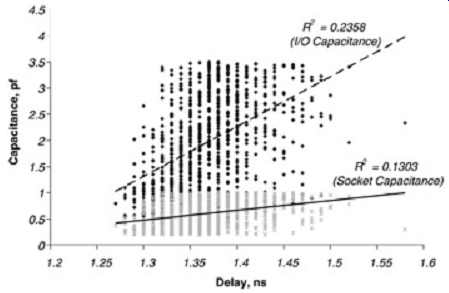
FIG. 18: Using IMC analysis to determine the significance and trends
of I/O and socket capacitance.
It should be noted these trends are feasible only when the system is well behaved. FIG. 19 is an IMC analyses for an ill-behaved system. Notice the distinctive gap in the scatter plot. This is because ringback becomes large enough that some of the iterations violate the switching threshold. Subsequently, the point where the ringback last crosses the threshold is considered the flight time. FIG. 20 is a representative waveform with a ringback violation taken from the Monte Carlo simulation. The points less than 1 ns are the delay measured at the rising edge when ringback does not violate the threshold region, and the points greater than 1 ns are the delay measured at the ringback violation when it occurs. If such patterns occur during a IMC analysis, the data should be analyzed to determine which variables are causing the system to be ill behaved. Steps should then be taken to confine those variables and the IMC should be repeated. As with all analysis, the designer must view the waveforms to ensure that the results are being interpreted correctly.
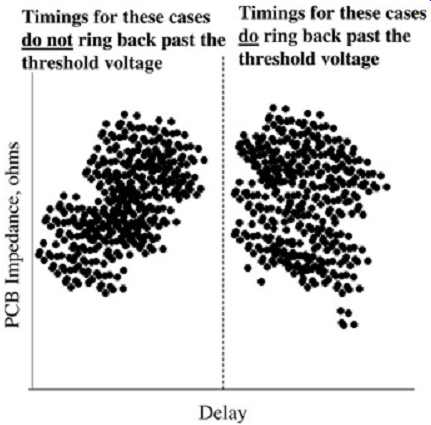
FIG. 19: Output of an IMC analysis when the system exhibits ringback
errors.
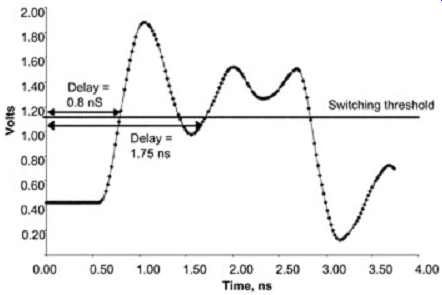
FIG. 20: Waveform from the IMC analysis depicted in FIG. 19 that shows
how ringback violations can cause a gap in the scatter plot.
After this initial analysis has been performed and all significance and trends have been analyzed, the worst-case corners should be identified and the variables should be prioritized.
The worst-case conditions (also known as corner conditions) should be identified for the following eight cases:
1. Maximum flight time
2. Minimum flight time
3. Maximum high-transition ringback
4. Maximum low-transition ringback
5. Maximum overshoot
6. Maximum undershoot
7. Maximum flight-time skew
8. Minimum flight-time skew
Furthermore, a list of the variables in decreasing order of significance (based on the linear fits described previously) should be created for each of the worst-case corners (known as a significance list). The significance list can help to prioritize the analysis and troubleshoot later in the design.
The maximum and minimum flight-time skews can be surmised from the flight-time plots because flight-time skew is simply the difference in flight times. The worst-case conditions should be determined assuming maximum variations possible for a given system. For example, the total variation over all processes for buffer impedance may vary 20% from part to part. However, impedance may not vary more than 5% for buffers on a single part.
Subsequently, if the maximum flight time skew occurs when the output impedance for the data net is high and the strobe impedance is low, the worst-case conditions should reflect only the maximum variation on a single part, not the entire process range for all parts (assuming that data and strobe are generated from the same part). In other words, when defining the worst-case conditions, be certain that you remain within the bounds of reality.
4.2. Ordered Parameter Sweeps
After the IMC analysis is complete and the eight corner conditions are determined, the solution space needs to be resolved. The solution space puts limits on all the variables that the designer has control of so that the system timing and signal integrity specifications are not violated. The ordered parameter sweeps are used to sweep one or two variables at a time systematically so that the behavior of the system can be understood and parameter limits can be chosen. All the fixed variables (the ones that are not being swept) should be set at the worst-case (corner) conditions during the sweeps. The worst-case conditions should be determined from the IMC analysis. FIG. 21 is an example of a three-dimensional parameter sweep (the topology is shown in FIG. 17) used to determine the maximum flight time. The fixed variables such as the I/O capacitance and the stub lengths were held constant at the worst-case values for maximum flight time while the motherboard and daughtercard impedance were swept in value. The values of this sweep are compared to the specifications. In this case it can readily be seen that the flight time increased dramatically when the motherboard impedance is greater than 60 ohm. The middle stub (daughtercard trace) causes the sudden increase in skew. As described in Section 5, as the impedance of the stub is decreased relative to the main bus trace impedance, the ledge moves down. The plot in FIG. 21 is flight time taken at a threshold voltage of Vcc/2. The sharp jump in flight time occurs when the ledge moves below the threshold voltage. FIG. 22 depicts waveforms at two different locations of the three-dimensional plot to show how the position of the ledge produces the three-dimensional shape. It is readily seen that the combination of the low stub impedance and the high board impedance pushed the ledge below the threshold voltage, causing an increase in the flight time equal to the length of the ledge.
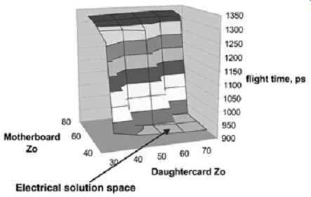
FIG. 21: Example of a three-dimensional ordered parameter sweep.
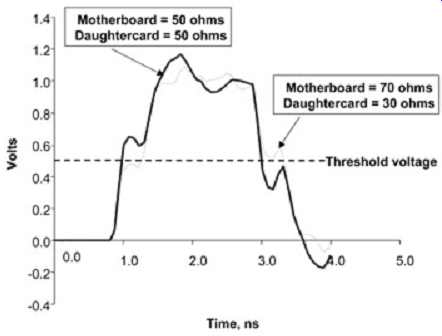
FIG. 22: Waveforms taken from the simulation that created the parameter
sweep in FIG. 21. Note the sudden increase in flight time when the ledge
moves below the threshold region.
Plots such as in Figures 9.21 and 9.23 are used to limit the solution space. For example, the plot shown in FIG. 23, which is simply the top view of FIG. 21, can be used to determine the impedance boundaries for both the motherboard and daughtercard trace so that the maximum flight time is not exceeded. In this case, assuming a maximum tolerable flight time of 1000 ps, the total impedance variation, including manufacturing variations and crosstalk, must be contained within the dashed line.
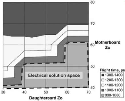
FIG. 23: Top view of FIG. 21. This view is useful in defining the solution
space.
The example shown in FIG. 23 will produce two solutions spaces:
1. 38 ? < daughtercard Zo < 70 ? and 40 ? < motherboard Zo < 52 ?
2. 58 ? < daughtercard Zo < 70 ? and 40 ? < motherboard Zo < 61 ?
Furthermore, it can be used to estimate the minimum spacing. Since the impedance is varied over a wide area, the maximum tolerable impedance variations can be translated into minimum spacing requirements by reverse engineering a SLEM model (the SLEM model is described in Section 3.6.2). A SLEM model translates crosstalk, which is a function of line- line spacing into an impedance variation. It is not difficult to translate an impedance variation into a spacing requirement for a given cross section. Note: Be certain that the manufacture impedance variations are accounted for when translating an impedance variation into a spacing requirement.
It is not necessary to use three-dimensional plots; however, they are generally more efficient than a two-dimensional approach. The parameter sweeps are then used to limit each variable that the designer has control of in order to choose the optimal electrical solution space. It is necessary to perform parametric sweeps for all relevant timing and signal quality metrics at each of the eight corners defined in Section .4.1. Often, custom scripts must be written to automate these sweeps efficiently. However, many simulation tool vendors are beginning to offer these capabilities.
4.3. Phase 1 Solution Space
The purpose of the phase 1 solution space is to limit the electrical solution space from infinite to finite. Subsequently, the simulations are simplified so that they can run fast.
Ordered parameter sweeps are performed on all the variables as described in Section 4.2 above.
To facilitate efficient and fast simulation times, several assumptions are made during phase 1.
1. SLEM transmission line models are used to account for crosstalk. The impedance is swept and the allowable impedance range is translated into an initial target impedance and spacing requirement. It is important to allow for manufacturer variations.
2. Power delivery and return paths are assumed to be perfect.
3. Simple patterns are used (no long pseudorandom patterns).
4. Simple linear buffers are used that are easy to sweep.
With these assumptions in place, the designer can quickly run numerous simulations to pick the topologies, the initial line lengths, minimum trace spacing, buffer impedances, termination values and PCB impedance values. Future simulations will incorporate the more computationally intensive effects. After the completion of the phase 1 solution space, the initial buffer parameters, such as impedance and edge rates, should be given to the silicon designers. This will allow them to design the initial buffers, which are needed for the phase 2 solution space.
Phase 1 ISI.
Intersymbol interference (ISI) also needs to be accounted for in the parameter sweeps. ISI is simply pattern-dependent noise or timing variations that occur when the noise on the bus has not settled prior to the next transition (see Section 4). To estimate ISI in a system, it is necessary to simulate long pseudorandom pulse trains. This technique, however, is long, cumbersome, and very difficult to do during a parameter sweep. The following technique will allow the designer to gain a first-order approximation of the ISI impact in the phase 1 solution space. The full effect of the ISI will be evaluated later.
To capture most of the timing impacts due to intersymbol interference, the parameter sweeps (for all eight worst-case corners) should be performed at the fastest bus frequency, and then at 2× and 3× multiples of the fastest bus period. For example, if the fastest frequency the bus will operate at produces a single bit pulse duration of 1.25 ns, the data pattern should be repeated with pulse durations of 2.5 and 3.75 ns. This will represent the following data patterns transitioning at the highest bus rate.
---010101010101010
---001100110011001
---000111000111000
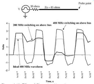
The timings should be taken at each transition for at least five periods so that the signal can reach steady state. The worst-case results of these should be used to produce the phase 1 solution space. This will produce a first-order approximation of the pattern-dependent impact on the bus design. This analysis can be completed in a fraction of the time that it takes to perform a similar analysis using long pseudorandom patterns. Additionally, since the worst signal integrity will often occur at a frequency other than the maximum bus speed, this technique helps ensure that signal integrity violations are not masked by the switching rate as in this Figure.
Monte Carlo Double Check.
After the phase 1 solution space is determined, it is a good idea to perform a final check.
Monte Carlo analysis can used as a double check on the phase 1 solution space to ensure passing margin under all conditions. Although the IMC analysis is designed to ensure that the parameter sweeps will yield the worst-case conditions, it is possible that the worst-case combination of variables was not achieved. During the Monte Carlo analysis, the results of the metric (i.e., the flight time or the skew) should be observed, as all the individual components of the design are bounded by the constraints of the phase 1 solution space and varied randomly. The maximum and minimum values should be compared to the specifications. If there are any violations, the specific conditions that caused the failure should be observed so that the mechanism can be established. Therefore, it is necessary to keep track of the Monte Carlo output and the random input variables so that a specific output can be correlated to all the input variables. It is sometimes useful to plot the output of the Monte Carlo analysis against specific variables as was done in the initial Monte Carlo analysis. This often provides significant insight into the cause of the failure.
Note that using Monte Carlo analysis as a double check will not necessarily capture any mistakes, so do not rely on it. Monte Carlo at this stage is simply a "shotgun blast in the dark"-maybe you will hit something and maybe you won't. If there is a mistake in your solution space, hopefully you will find it.
4.4. Phase 2 Solution Space
The phase 2 solution space in an incremental step toward the final solution space. In the phase 1 solution space, many approximations were made to quickly limit the major variables of the solution space. In the development of the phase 2 solution space, a limited set of simulations are performed near the edges of the phase 1 solution space. These simulations should contain fully coupled transmission lines instead of a SLEM approximation. IBIS or transistor models should be used in place of the linear buffer models, and full ISI analysis with pseudorandom patterns should be used.
Phase 2 solution space augments the phase 1 solution space by removing some of the approximations as listed below.
1. The SLEM models should be replaced by fully coupled transmission line models with the minimum line-line spacing. Remember that the minimum spacing was determined from the impedance sweeps in the phase 1 solution space by observing maximum and minimum impedance variations. A minimum of three lines should be simulated, with the middle line being the target net.
2. A long pseudorandom bit pattern should be used in the simulation to determine the impact of ISI more accurately. This pattern should be chosen to maximize signal integrity distortions by switching between fast and slow data rates and between odd- and even-mode switching patterns.
3. The linear buffers should be replaced with full transistor or IBIS behavioral models.
The phase 2 solution space will further limit the phase 1 solution space. Again, after the completion of phase 2, it is a good idea to perform a large Monte Carlo simulation to double check the design space.
Eye Diagrams Versus Parameter Plots.
During the phase 1 analysis, parameter plots are used to limit the large number of variables in the system. Since many approximations are made, it is relatively simple to create a UNIX script or write a C++ program to sort though the output data from the simulator and extract the timings from the waveforms. Furthermore, some interconnect simulation suites already have this capability built in. Parameter plots are very efficient when running extremely large sets of simulations because they are faster and they consume significantly less hard-drive space that an eye diagram sweep. Furthermore, parameter plots give the designer an instant understanding of the trends.
An eye diagram is created by laying individual periods of transitions on a net on top of each other. An eye diagram is useful for analyzing individual, more complicated simulations (not sweeps) with randomized data patterns. The main advantage of an eye diagram is that it is more reminiscent of a laboratory measurement, and several useful data points can be obtained simply by looking at the eye. The disadvantage is that they are cumbersome, not well suited to the analysis of many simulations, and do not provide an easy way to separate out silicon- and system-level effects.
FIG. 24 depicts an example of an eye diagram from a phase 2 source synchronous simulation. The strobe is superimposed on top of the data eye. Several effects are easily identifiable. The total setup and hold windows are determined simply by measuring the time between the strobe and data at the upper or lower portion of the noise margin. If the setup/hold windows are greater than the receivers setup/hold requirements, then the timing margin is positive. Furthermore, the ringback margin can be determined simply by observing how close the signal rings back toward the threshold voltage. It should be obvious that eye diagrams are not particularly suited for sweeping, or for evaluation of flight time or flight-time skews. However, many engineers prefer to utilize them in the later stages of the design.
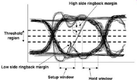
FIG. 24: Example of an eye diagram.
Phase 2 ISI.
The evaluation of ISI can be tricky. To do so, it is necessary to perform targeted simulations at the edge of the design space using a long pseudorandom pulse train. If pattern-dependent timing or signal quality violations occur, steps should be taken to minimize reflections on the bus; this will reduce the ISI. Usually, the best way to limit reflections on the bus is to tighten up the impedance variations and minimize discontinuities by shortening stubs and connectors and matching impedances between packages and PCBs. The results of the ordered sweeps and the significance list should be quite helpful at this stage. Also, be sure to include any startup strobe ISI in the analysis. Usually, strobes do not exhibit ISI because they operate in a single pattern. However, often the strobe is turned off until it is time for the component with which it is associated to drive signals onto the bus. It will take several transitions for the strobe to reach steady state. If the bus protocol allows valid signals to be driven onto the bus before the strobe can reach steady state, the strobe ISI can significantly affect the timings by increasing skew.
The worst-case ISI can be evaluated using the following steps:
1. Simulate the longest net in the bus with the most impedance discontinuities using a long pseudorandom bit pattern for each of the worst-case conditions (i.e., they should be at the edge of the solution space so far defined).
2. Take the flight time of the first transition of the ISI simulation as a baseline.
3. Determine the rising and falling flight times for each bus transition (using the standard load as a reference).
4. Subtract the minimum and maximum delays from the baseline delays and find the worst-case difference.
5. Take the smallest negative and the greatest positive difference. This should be the worst-case ISI impact on timings.
6. Simulate the maximum and minimum flight time and flight-time skew corners with a very slow switching rate that settles completely prior to each transition and add the numbers from step 5 to the results. This should represent the worst-case phase 2 flight time and flight-time skew numbers that should be included in the spreadsheet.
Remember to account for the startup ISI on the strobe if necessary.
7. Look for the worst-case overshoot, undershoot, and ringback, and make sure that they do not violate the threshold region or exceed maximum overshoot specifications.
The alternative method is to use an eye diagram. Note that if an eye diagram is used, the total timings measured will already incorporate ISI.
4.5. Phase 3 Solution Space
The phase 1 and phase 2 solution spaces have significantly narrowed the solution space.
Targets for all aspects of the design should be defined. The phase 3 solution space is the final step. Phase 3 should include the effects that are very difficult to model. The timing impacts from these effects should already be incorporated into the design due to the Vref uncertainty (remember, when choosing the noise margin, many of the effects that are difficult or impossible to simulate are included). Subsequently, it is important that the noise margin be appropriately decreased when simulating phase 3 effects. For example, if the initial estimate was that I/O level power delivery effects will cause 40 mV out of 100 mV total noise, the noise margin should be decreased to 60 mV when calculating timings with a power delivery model in place. Often, if the designer is confident that the noise margin accounts adequately for these effects, phase 3 is not necessary except as a double check. The phase 3 analysis builds on phase 2 and adds in the following effects:
1. I/O level power delivery (Section 6)
2. Nonideal current return paths (Section 6)
3. Simultaneous switching noise (Section 6)
Typically, each of the eight corner conditions (they must represent the absolute corners of the design space determined with phase 2) defined in Section 9.4.1 are simulated with power delivery, SSN and return path models. It should be noted, however, that a clean design should not exhibit any nonideal return paths because they are very difficult to model and can significantly affect the performance of the system.
If the rest of the design has been done correctly (i.e., the power delivery system has been designed properly and no nonideal return paths are designed into the system), this stage of the design will affect the design minimally. That is, the excess timings due to the original noise margin assumptions should be greater than or equal to the timing impact of the phase 3 analysis after the noise margin has been decreased adequately.
5. DESIGN GUIDELINES
The output of the sensitivity analysis and the layout study are used to develop the design guidelines. The guidelines should outline every parameter of the design that is required to meet the timing specifications. These guidelines are used to produce a high-volume design that will operate under all manufacturer and environmental variations. A subset of the guidelines should include the following:
1. Maximum and minimum tolerable buffer impedance and edge rates
2. Tolerable differences between rising and falling edge rates and impedances for a given chip
3. Maximum and minimum package impedance and lengths
4. Required power/ground-to-signal ratio and optimal pin-out patterns for packages and connectors
5. Maximum and minimum socket parasitics and possibly height
6. Maximum and minimum termination values
7. Maximum and minimum connector parasitics
8. Specific topology options including lengths
9. Maximum stub lengths (this may be the same as the package length, or it could be a daughtercard trace)
10. Impedance requirements for the PCB, package, and daughtercard.
11. Minimum trace-trace spacing
12. Minimum serpentine lengths and spacing
13. Maximum variation in lengths between data signals and strobes
14. Plane references (As discussed in Section 6)
15. I/O level power delivery guidelines (see Section 6)
6. EXTRACTION
After the system has been designed and the package and PCB board routed, the final step is to examine the layout and extract the worst-case nets for the eight corners. These specific corners should be fully simulated using the phase 3 techniques to ensure that the design will work adequately. The significance list should help choose the worst-case nets. However, the following attributes should be examined to help identify the worst-case nets:
1. Signal changing layers
2. Significant serpentine
3. High percentage of narrow trace-trace spacing
4. Longest and shortest nets
5. Longest stub
6. Longest and shortest package lengths
7. Impedance discontinuities
7. GENERAL RULES OF THUMB TO FOLLOW WHEN DESIGNING A SYSTEM
As high-speed digital systems become more complex, it is becoming increasingly difficult to manage timings and signal integrity. The following list is in no particular order, but if followed, will hopefully make the design process a little simpler:
1. Early discussions between the silicon and system designers should be held to choose the best compromise between die ball-out and package pin-out. Often, the die ball out is chosen without consideration of the system design. The package pin-out is very dependent on the die ball-out, and an inadequate package pin-out can cause severe difficulties in system design. Many designs have failed because of inadequate package pin-out.
2. When designing a system, make certain that the reference planes are kept continuous between packages, PCBs, and daughtercards. For example, if a package trace is referenced to a VDD plane, be certain that the PCB trace that it is connected to is also referenced to a VDD plane. Often, this is not possible because of package pin-out.
This has been the cause of several failures. It is very expensive to redesign a board and/or a package to fix a broken design.
3. Be certain that a strobe and its corresponding data are routed on the same layer.
Since different layers can experience the full process variations, this can cause significant signal integrity problems.
4. Be certain that any scripts written to automate the sweeping function are working properly.
5. Make a significant effort to understand the design. Do not fall into the trap of designing by simulation. Calculate the response of some simplified topologies by hand using the techniques outlined in this book. Make certain that the calculations match the simulation. This will provide a huge amount of insight, will significantly help troubleshoot problems, and will expedite the design process.
6. Look at your waveforms! This may be the most important piece of advice. All too often, I have seen engineers performing huge numbers of parameter sweeps, looking at the three-dimensional plots and defining a solution space. This does not allow for an intimate understanding of the bus and often leads to an ill-defined solution space, wasting an incredible amount of time. Furthermore, when a part is delivered that does not meet the initial specifications, or a portion of the design changes, the engineer may not understand the impact to the design. It is important to develop and maintain basic engineering skills and not use algorithms in place of engineering. Double check your sweep results by spot checking the waveforms.
7. Keep tight communication with all disciplines, such as EMI and thermal.
8. Plan your design flow from simple to complicated. Initiate your design by performing hand calculations on a simplified topology. Increase the complexity of the simulations by adding one effect at a time so that the impact can be understood. Do not move on until the impact of each variable is understood.
9. Compensate for long package traces by skewing the motherboard routing lengths.
When matching trace lengths to minimize skew, it is important that the electrical length from the driver pad (on the silicon) to the receiver pad be equal. If there is a large variation in package trace lengths, it is usually necessary to match the lengths by skewing the board traces. Subsequently, the total paths from silicon to silicon are equal lengths.