FIG. 25
| Home | Audio mag. | Stereo Review mag. | High Fidelity mag. | AE/AA mag. |
For non-critical amplifier applications, and as the basis of many types of oscillator, CMOS I.C.s are a very attractive proposition due to the simplicity of the circuitry and their low cost.
Simple Amplifier
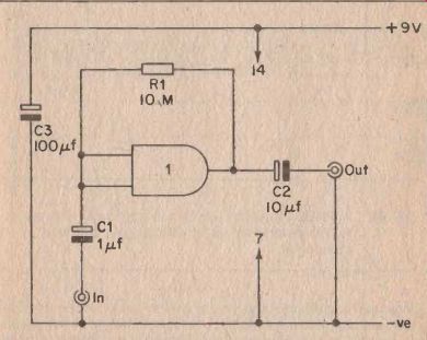
The circuit diagram of a very simple CMOS amplifier which uses a single inverter is shown in Figure 25. R1 is used to bias the inverter as a linear amplifier. The output of the device will begin to go high when the supply is initially connected, since the input will be low. When the voltage at the output reaches the transfer voltage of the gate, the input will try to take the output low as the input will be taken high by the voltage obtained via R1 from the output. The output voltage will be stabilized at about half the supply potential by this negative feedback action. The gate is thus biased into a linear mode.
FIG. 25
Basic CMOS linear amplifier
At audio frequencies this circuit offers a voltage gain of about 50 times, and even at a frequency of many MHz it will still provide a degree of gain. It is not intended for use in Hi-Fi circuits, and is really only suitable for non -critical applications, such as in the peak level indicator which was described earlier.
The value of R1 is not critical, but it should be in the Megohm region if the full voltage gain of the circuit is to be realised. C1 and C2 are the input and output D.C. blocking capacitors respectively. It is not a good idea to use this circuit with a nominal supply voltage of less than about 9 V as it could then become unstable.
Operational Amplifier
A more sophisticated amplifier can be produced by cascading three inverters together, as shown in Figure 26. This circuit is biased into a linear operating condition by R2, which operates in much the same way as R.1 of Figure 25.
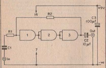
FIG.
26 A CMOS amplifier which uses op. amp techniques for the determination of
voltage gain and input impedance.
Operational amplifier techniques are used to select the desired input impedance and voltage gain of the circuit, and this makes the circuit very versatile indeed. The input impedance of the circuit is equal to the value given to R1, and the value of R2 is calculated by multiplying that of R1 by the required voltage gain.
Input impedances in the Megohm region are easily attained, as are very high voltage gains, but it is not really practical to obtain both of these in the same amplifier. There is the problem that the necessary high value resistor for R2 would simply not be obtainable, and stability which was described earlier.
The value of R1 is not critical, but it should be in the Megohm region if the full voltage gain of the circuit is to be realised. C1 and C2 are the input and output D.C. blocking capacitors respectively. It is not a good idea to use this circuit with a nominal supply voltage of less than about 9 V as it could then become unstable.
Crystal Oscillator
Crystal oscillators have been used since the early days of entertainment broadcasting whenever a highly stable R.F. oscillator is required. They are probably used more now than at any time in the past, and apart from use in crystal calibration oscillators and similar radio applications they are often used in digital clocks and other digital equipment where they generate a stable timebase signal.
CMOS I.C.s can be used as the active devices in good quality crystal oscillators having operating frequencies up to about 10 MHz or so.
Figure 27 shows the circuit diagram of a simple CMOS crystal oscillator which uses a couple of inverters.
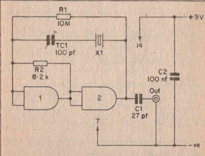
FIG. 27 A simple crystal oscillator
The two inverters are used to provide an amplifier which has its input and output of the amplifier via T C1, and at the series resonant frequency of the crystal (where it has a very low impedance) positive feedback will be applied to the circuit and it will oscillator.
T C1 enables the oscillation frequency of the circuit to be finely trim med to the nominal frequency of the crystal. If this feature is not required T C1 can be omitted, with the crystal then being connected in parallel with R1.
At first sight R1 may appear to perform no useful function, but it was found to be necessary to add this as otherwise the oscillator often failed to start when power was applied to the circuit. C1 is the output D.C. blocking Capacitor and C2 is a supply decoupling capacitor.
This circuit seems to operate satisfactorily over a wide range of frequencies with the component values shown, and the prototype oscillated properly with any crystal having a frequency from a few tens of kHz to many MHz.
Pierce Oscillator
It is possible to use a single inverter to provide the basis of a crystal oscillator, and such a circuit appears in Figure 28.
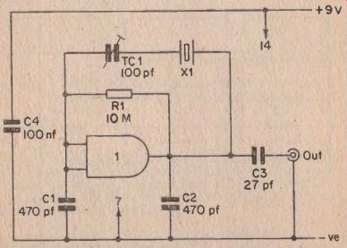
-- Figure 28. A CMOS Pierce oscillator.
This uses the well known Pierce oscillator configuration.
The two inverters are used to provide an amplifier which has its input and output of the amplifier via TC1, and at the series resonant frequency of the crystal (where it has a very low impedance) positive feedback will be applied to the circuit and it will oscillator.
TC1 enables the oscillation frequency of the circuit to be finely trim
med to the nominal frequency of the crystal. If this feature is not required T C1 can be omitted, with the crystal then being connected in parallel with R1 .
At first sight R1 may appear to perform no useful function, but it was found to be necessary to add this as otherwise the oscillator often failed to start when power was applied to the circuit. C1 is the output D.C. blocking capacitor and C2 is a supply decoupling capacitor.
This circuit seems to operate satisfactorily over a wide range of frequencies with the component values shown, and the prototype oscillated properly with any crystal having a frequency from a few tens of kHz to many MHz.
The inverter is biased into a linear amplifying mode by R1, and the crystal is connected between the input and the output of the circuit by way of T C1. This circuit, like the previous design, operates at the series resonant frequency of the crystal.
There is no obvious positive feedback loop between the output and input of the circuit, just the opposite in fact, since the input and output of the amplifier are in antiphase. At series resonance it would appear as though the crystal provides negative feedback to the amplifier.
This is not actually the case since C1 and C2 form a capacitive centre tap on the crystal, with the centre tap being earthed. The crystal thus acts as a sort of transformer at series resonance, with its two connections in antiphase. There is therefore a 180 degree phase shift through both the amplifier and the crystal, and the feedback is positive.
T C1 is used to trim the oscillation frequency of the circuit to the crystal's nominal frequency, and again, this feature can be left out if desired. T C1 is then omitted and the crystal is connected across R1.
C1 and C2 are shown as having values of 470 pF each in the circuit diagram. Using these values the circuit should oscillate satisfactorily over a wide range of frequencies. At frequencies above a few MHz it may be necessary to reduce the value of these components somewhat in order to obtain oscillation. Conversely, at frequencies below a few hundred kHz a slightly higher value may be required for these components. Also, if maximum output is required it will be necessary to find the values of these capacitors by empirical means.
L-C Oscillator
A crystal oscillator is, of course, intended to provide high stability at a single frequency, and is of no use if a tuneable wide range oscillator is required. This category of oscillator is almost invariably of the L-C variety for operating frequencies of a few hundred kHz and above. CMOS I.C.s can be used as the basis of simple L-C oscillators, and an example of such a circuit is shown in Figure 29.
This operates at a frequency of around 465 kHz, and T1 is an ordinary broadcast receiver I.F. transformer. In normal use the tuned winding is the primary and the untuned one is the secondary, but here the windings are used in the opposite roles. This is just a simple feedback circuit with the CMOS inverter being used as a linear amplifier. The circuit can be tuned over a fairly narrow range of frequencies by means of VC1.
As it stands here, the circuit is suitable for use as an I.F. alignment generator or as a B.F.O. for a communications receiver. However, it will work at frequencies beyond 10 MHz if a suitable coil is used (virtually any coil with a tuned winding plus a low impedance winding).
The inverter is biased into a linear amplifying mode by R1 , and the crystal is connected between the input and the output of the circuit by way of T C1. This circuit, like the previous design, operates at the series resonant frequency of the crystal.
There is no obvious positive feedback loop between the output and input of the circuit, just the opposite in fact, since the input and output of the amplifier are in antiphase. At series resonance it would appear as though the crystal provides negative feedback to the amplifier.
This is not actually the case since C1 and C2 form a capacitive centre tap on the crystal, with the centre tap being earthed. The crystal thus acts as a sort of transformer at series resonance, with its two connections in antiphase. There is therefore a 180 degree phase shift through both the amplifier and the crystal, and the feedback is positive.
T C1 is used to trim the oscillation frequency of the circuit to the crystal's nominal frequency, and again, this feature can be left out if desired. T C1 is then omitted and the crystal is connected across R1 .
C1 and C2 are shown as having values of 470 pF each in the circuit diagram. Using these values the circuit should oscillate satisfactorily over a wide range of frequencies. At frequencies above a few MHz it may be necessary to reduce the value of these components somewhat in order to obtain oscillation. Conversely, at frequencies below a few hundred kHz a slightly higher value may be required for these components. Also, if maximum output is required it will be necessary to find the values of these capacitors by empirical means.
L-C Oscillator
A crystal oscillator is, of course, intended to provide high stability at a single frequency, and is of no use if a tuneable wide range oscillator is required. This category of oscillator is almost invariably of the L -C variety for operating frequencies of a few hundred kHz and above. CMOS I.C.s can be used as the basis of simple L-C oscillators, and an example of such a circuit is shown in Figure 29.
This operates at a frequency of around 465 kHz, and T1 is an ordinary broadcast receiver I.F. transformer. In normal use the tuned winding is the primary and the untuned one is the secondary, but here the windings are used in the opposite roles. This is just a simple feedback circuit with the CMOS inverter being used as a linear amplifier. The circuit can be tuned over a fairly narrow range of frequencies by means of VC1.
As it stands here, the circuit is suitable for use as an I.F. alignment generator or as a B.F.O. for a communications receiver. However, it will work at frequencies beyond 10 MHz if a suitable coil is used (virtually any coil with a tuned winding plus a low impedance winding).
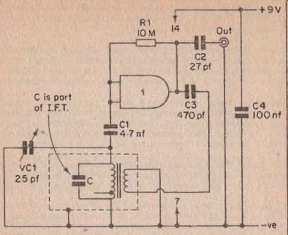
FIG. 29 A simple L-C oscillator By increasing the value of VC1 to a few hundred
pF the circuit can also be made to cover a wide tuning range. Note that the
circuit will not oscillate unless T1 is connected with the phasing shown in
the circuit diagram.
The circuit will operate over a frequency range of a few hundred kHz to more than 10 MHz, and the values of L and C are selected to suit the desired operating frequency. C can be a variable capacitor if a variable frequency oscillator is required. Note that the tapping does not have to By increasing the value of VC1 to a few hundred pF the circuit can also be made to cover a wide tuning range. Note that the circuit will not oscillate unless T1 is connected with the phasing shown in the circuit diagram.
Hartley Oscillator
A CMOS inverter can be used in the well known Hartley type oscillator, and this has the advantage over the previous design that only a single winding is needed on the coil. However, this must be a centre tapped winding. The circuit diagram of a CMOS Hartley oscillator is shown in Figure 30.
This is very similar in operation to the pierce oscillator which was described earlier, the main difference being that a centre tapped L -C circuit is used in place of the capacitively centre tapped crystal. The coil provides a D.C. path between the input and output of the inverter, and so no bias resistor is needed.
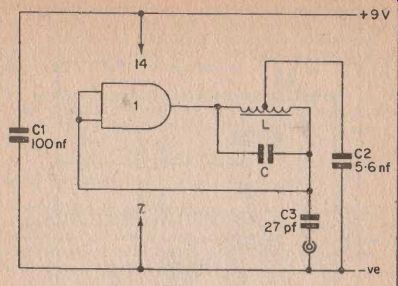
FIG. 30. A CMOS Hartley oscillator circuit
The circuit will operate over a frequency range of a few hundred kHz to more than 10 MHz, and the values of L and C are selected to suit the desired operating frequency. C can be a variable capacitor if a variable frequency oscillator is required. Note that the tapping does not have to be at precisely the centre of the winding, and that for instance, the circuit will operate perfectly well using the primary of an I.F. transformer.
Phase Shift Oscillator
An audio squarewave generator was covered in the previous SECTION, and this is not the only type of audio waveform generator which can be produced using CMOS inverters. It is possible to generate a sinewave using a phase shift oscillator, and such a circuit is shown in Figure 31.
Here three inverters are wired in cascade to form a high gain inverting amplifier. The actual gain of the circuit is controlled by the feedback network consisting of R1 and R4. R1 has been made variable so that the gain of the circuit can be set at precisely the required amount.
The output of the amplifier is coupled to the input by way of the three 60 degree phase shift networks which consists of C4 - R2, C5 - R3, C6 - R4. Thus, at the operating frequency of this network there is positive feedback between the input and output of the circuit, and provided the gain of the amplifier is sufficient, the circuit will oscillate. The gain should be no more than is absolutely necessary as otherwise the output waveform will be distorted. R1 is therefore adjusted for the lowest resistance that provides reliable oscillation.
An operating frequency of about 1 kHz is obtained with the specified values in the phase shift networks. This can be altered if required, by be at precisely the centre of the winding, and that for instance, the circuit will operate perfectly well using the primary of an I.F. transformer.
Phase Shift Oscillator
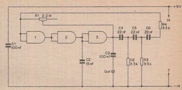
FIG. 31 A 1 kHz phase shift oscillator circuit.
An audio squarewave generator was covered in the previous SECTION, and this is not the only type of audio waveform generator which can be produced using CMOS inverters. It is possible to generate a sinewave using a phase shift oscillator, and such a circuit is shown in Figure 31.
Here three inverters are wired in cascade to form a high gain inverting amplifier. The actual gain of the circuit is controlled by the feedback network consisting of R1 and R4. R1 has been made variable so that the gain of the circuit can be set at precisely the required amount.
The output of the amplifier is coupled to the input by way of the three 60 degree phase shift networks which consists of C4 - R2, C5 - R3, C6 - R4. Thus, at the operating frequency of this network there is positive feedback between the input and output of the circuit, and provided the gain of the amplifier is sufficient, the circuit will oscillate. The gain should be no more than is absolutely necessary as otherwise the output waveform will be distorted. R1 is therefore adjusted for the lowest resistance that provides reliable oscillation.
An operating frequency of about 1 kHz is obtained with the specified values in the phase shift networks. This can be altered if required, by changing the values of C4 to C6. These should always be equal in value, and their value is inversely proportional to the operating frequency of the circuit. Thus using 220 nF capacitors gives an operating frequency of about 100 Hz, and 2.2 nF capacitors would provide oscillation at about 10 kHz. The circuit will function satisfactorily over a frequency range of less than 1 Hz to more than 20 kHz.
C2 is a stabilization capacitor and C3 provides output D.C. blocking.
The value of C3 should be increased if the unit is used to feed a fairly low impedance or if it is used at a lower operating frequency than 1 kHz.
Schmitt Trigger Oscillator
The circuit diagram of this unusual circuit is shown in Figure 32. The three inverters are connected as a form of Schmitt trigger, and this type of circuit is fully dealt with in the following SECTION. Therefore only the characteristics of the Schmitt trigger circuit will be considered, rather than how this circuit actually operates.
A Schmitt trigger has an output which has only two stable states, and in this case the output is normally high. By applying a suitable input voltage the output can be made to go to the low state. With this circuit the input must be taken to about half the supply rail potential before the output will be triggered to the low state.
The output will return to the high state again if the input voltage is reduced to a suitable level, but the voltage at which the circuit triggers back to the high state is less than the original threshold voltage. This feature is termed hysteresis.
It is quite simple to understand the way in which this circuit operates.
The output goes to the high state when the supply is initially connected since the input will be low. Capacitor C then begins to charge up via resistor R. When the voltage across C reaches the upper trigger threshold voltage, the output of the circuit goes low. C then begins to discharge through R and the output circuitry of inverter 3. When the voltage across C equals the lower threshold voltage of the Schmitt trigger, the output of the circuit will go high.
C then begins to charge via R once again until the voltage across C reaches the upper threshold voltage of the circuit. The output then goes low again. C then begins to discharge, and the circuit continuously oscillates in this fashion for as long as power is applied to it.
Two output waveforms are generated, a squarewave at the output of inverter 3, and a triangular waveform at the junction of R and C.
Variations in output load Impedance and supply voltage result in comparatively large variations in operating frequency, and so in critical applications it is necessary to use a buffer amplifier at the output and a stabilized power supply.
changing the values of C4 to C6. These should always be equal in value, and their value is inversely proportional to the operating frequency of the circuit. Thus using 220 nF capacitors gives an operating frequency of about 100 Hz, and 2.2 nF' capacitors would provide oscillation at about 10 kHz. The circuit will function satisfactorily over a frequency range of less than 1 Hz to more than 20 kHz.
C2 is a stabilization capacitor and C3 provides output D.C. blocking.
The value of C3 should be increased if the unit is used to feed a fairly low impedance or if it is used at a lower operating frequency than 1 kHz.
Schmitt Trigger Oscillator
The circuit diagram of this unusual circuit is shown in Figure 32. The three inverters are connected as a form of Schmitt trigger, and this type of circuit is fully dealt with in the following SECTION. Therefore only the characteristics of the Schmitt trigger circuit will be considered, rather than how this circuit actually operates.
A Schmitt trigger has an output which has only two stable states, and in this ease the output is normally high. By applying a suitable input voltage the output can be made to go to the low state. With this circuit the input must be taken to about half the supply rail potential before the output will be triggered to the low state.
The output will return to the high state again if the input voltage is reduced to a suitable level, but the voltage at which the circuit triggers back to the high state is less than the original threshold voltage. This feature is termed hysteresis.
It is quite simple to understand the way in which this circuit operates.
The output goes to the high state when the supply is initially connected since the input will be low. Capacitor C then begins to charge up via resistor R. When the voltage across C reaches the upper trigger threshold voltage, the output of the circuit goes low. C then begins to discharge through R and the output circuitry of inverter 3. When the voltage across C equals the lower threshold voltage of the Schmitt trigger, the output of the circuit will go high.
C then begins to charge via R once again until the voltage across C reaches the upper threshold voltage of the circuit. The output then goes low again. C then begins to discharge, and the circuit continuously oscillates in this fashion for as long as power is applied to it.
Two output waveforms are generated, a squarewave at the output of inverter 3, and a triangular waveform at the junction of R and C. Variations in output load impedance and supply voltage result in comparatively large variations in operating frequency, and so in critical applications it is necessary to use a buffer amplifier at the output and a stabilized power supply.
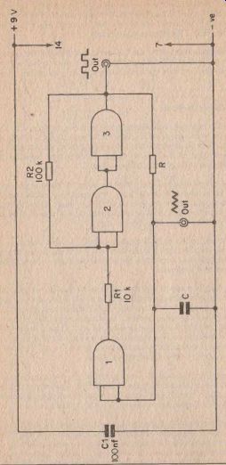
FIG. 32 A Schmitt trigger oscillator
An unusual feature of this circuit is the wide frequency coverage which can be obtained in a single range if R is a variable resistor. For example, using a 2.2 M-o potentiometer for R and a 470 nF capacitor for C, the circuit has an operating range of a few Hz to many tens of kHz.
The circuit will oscillate at a frequency of about 1 kHz with C at 100 nF and R at 470 k.
A peak to peak output amplitude virtually equal to the supply rail potential is obtained at the squarewave output, but the triangular output amplitude is much lower, being something in the region of 100 mV peak to peak. Also, the triangular output is at a relatively high impedance unless R has a low value. The circuit will oscillate with R having a value as low as a few tens of ohms, but for maximum reliability it should have a value of a few hundred ohms or more (the upper limit being many Megohms).
An unusual feature of this circuit is the wide frequency coverage which can be obtained in a single range if R is a variable resistor. For example, using a 2.2 Megohm potentiometer for R and a 470 nF capacitor for C, the circuit has an operating range of a few Hz to many tens of kHz.
The circuit will oscillate at a frequency of about 1 kHz with C at 100 nF and R at 470 k.
A peak to peak output amplitude virtually equal to the supply rail potential is obtained at the squarewave output, but the triangular output amplitude is much lower, being something in the region of 100 mV peak to peak. Also, the triangular output is at a relatively high impedance unless R has a low value. The circuit will oscillate with R having a value as low as a few tens of ohms, but for maximum reliability it should have a value of a few hundred ohms or more (the upper limit being many Megohms).