by JAMES BOAK, Contributing Editor
A versatile circuit for regulated DC in quantity, by James E. Boak.
ONE OF THE MOST POPULAR power amps to appear in The Audio Amateur is Reg Williamson's classic, the 20/20 (TAA 1/70, p. 51. The amp's clean performance and ease of construction have kept interest high, and several people have attempted to design power supply circuits to gild its characteristics.
Reg published the first of these circuits with the original construction article. His aim was to protect the output transistors in the event of an overload by shutting down the power supply. This was a latching circuit; you had to power down or "reset" the protection after removing the overload.
The next circuit to reach The Audio Amateur's pages was a true regulator, josh Goldberg's 68V supply (TAA 2/74, p. 13). The design featured straight volt-amp limiting at a fixed value.
Although each circuit had something to recommend it, drawbacks to each, in both function and design, limited their usefulness.
The Williamson design did not provide regulation; the Goldberg design lacked "foldback" limiting (a very important consideration if the supply overload circuit is to protect the output transistors as well(. I was tottering on the brink of designing a rugged, three-terminal type regulator with adjustable foldback current limiting, internal safe-area and thermal shutdown protection, and adjustable output voltages, when Nelson Pass's class A amp arrived ( TAA 4/78, p. 4).
The Pass amp has supply demands somewhat like the Williamson 20/20.
The ±32 volt rails of the split supply correspond to the 60 to 68 volts we find on the Williamson amp. The class A amp of course draws more current, even when both are at full load. But due to the split supplies Pass uses on his amp, the overall maximum output is about 300 watts in each case (32 volts at 8 amps vs. 68 volts at 4 amps).
"Wait a minute!" I can hear you saying. "Isn't one of the benefits of a class A amp the constant load it presents to its supply? Why regulate it at all?" The reason for regulation is that Pass has chosen a bipolar push-pull design. With three current paths and a full load current much greater than the idle current, the amp looks like a class B load (plus a constant) to the power supply. The price we pay for the amp's increased efficiency is this load current variation. To provide low noise at no signal, and to maintain voltage levels within the amp, we still have to regulate the supply.
Another reason to design a regulated supply is the Williamson 40/40 [see p. 5, TAA 4/79]. This comprehensive update of the earlier 20/20 has very similar supply demands.
The final and most compelling reason, however, is my own forth coming 80 watt 541-based power amp. I required a large and tightly regulated supply for this amp, to keep the dissipation under control while working near the absolute maximums for the 541 package. The sup ply demands range upwards to about 8A peak at ±40VDC, or somewhere between the large current demands of the Pass design and the voltage requirements of the Williamson amp.
Rarely in the demanding world of quality audio design can one kill two birds, let alone three, with one stone.
I found the temptation irresistible, and the result is the circuit described in this article.
DESIGNING THE SUPPLY
I feel that the fewer parts a design re quires, the fewer parts there are to go wrong. This leads me to design with IC components wherever they can be used without sacrificing performance. I further believe a good design is straightforward and easily comprehensible. When a designer thoroughly understands his circuit, he can more easily analyze and correct those factors which degrade performance.
We therefore want to start with a simple IC circuit, adding complexity only where necessary to ensure performance. Anyone who has worked with a three-terminal monolithic IC regulator appreciates the reliability and ease of use of these devices: once installed, they are virtually immune to overload and overheating. We will therefore start with a three-terminal regulator as our basic circuit.
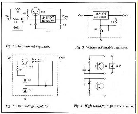
This certainly satisfies the simplicity criterion, but what about performance? The first problem we en counter is the output current, as most available regulators are limited to about 1.5 amps. We can increase the current capacity of the regulator with the Fig. 1 circuit. The ratio R2/R1 sets the ratio of currents through the regulator: i.e., if R2 = 6 and R, = 2, then the transistor TR, will pass 3 amps when the regulator passes 1 amp. Output currents in excess of 20 amps are possible with a suitable TR1. As long as we select a transistor with a wattage rating WT such that WT/WR > R2/R1, where WR is the wattage rating of the regulator (about 20 watts for an LM340T), and put both TR, and the regulator on a common heatsink, we can treat the combination circuit just like a monolithic regulator, with dissipation and current capacity equal to the sum of the elements. The regulator's output impedance is divided by the ratio R2/R, The regulator will be thermally protected for any size of heatsink, and will have foldback current limiting and safe area protection.
The circuit still will not do the required job, however. The output voltage is fixed at the regulator voltage, and that limits us to a maximum of 24 volts.
This is the voltage above the ground pin; we can therefore raise the output voltage by raising the ground potential of the regulator IC.
This can be done with any stable voltage capable of sinking about 10mA of class A current. In order to improve stability, I "bootstrap" this reference with an additional 15mA of current from the output.
We must also ensure that at no time does the voltage across the regulator exceed 35 volts, as the internal pass transistor in the IC would be damaged if this occurred. We need to protect against high input voltage, and we need to reduce the input voltage if the output is shorted. We can accomplish this by adding a "pre regulator" which is really just an emitter-follower regulator (see Fig. 2( placed ahead of the IC.
Under normal conditions, no matter what the input voltage, the IC sees a constant supply voltage equal to zener voltage Z,. In the event of a short circuit, D, is turned on by the drop-in output potential drop relative to the floating "ground" pin of REG,.
This shorts the bootstrapped zener reference Z2, reducing the voltage across REG, to about Z,'s value.
The only feature we need add is the ability to vary the output voltage in order to trim the regulated output and allow for component variations We can do this by adding a variable resistance in the ground leg of REG, as in Fig. 3. Using a 500 Ohm pot with total ground current of about 25mA allows us to vary the output voltage by a total of 6-8 volts (limited by Z,) GILDING THE COMPLETED DESIGN The basic design approach is complete. One or two chores remain however. We must ensure that the ground reference is free of stray AC which would appear on the output; a tantalum cap across Z2 takes care o this. An additional problem arise due to the current Z2 must sink. In the 68 volt configuration, Z2 must sink not only the 25mA class A and bootstrap current, but also the current through the pre-regulator, which will be about 20mA. This means Z; must dissipate nearly 2 watts.
The typical zener impedance of < 47 volt device is 100 Ohm, which would cause the ground reference to vary significantly with current despite the bootstrap. To avoid this we use the zener power booster of Fig. 4. This circuit has two advantages. First, the dissipation of the "zener" equals the transistor dissipation. We can build zeners with dissipations of hundred; of watts using this technique. Second the zener impedance is divided by the hfe of the transistor. Thus, for a 47 volt zener with 10012 impedance and a transistor with h„ of 100, the resulting "zener" impedance will be only 1.012, resulting in a shift of only 1mV per mA sink current shift.
Combining all these tricks, we come to the Fig. 5 circuit, which can provide up to 10 amps at 68 volts using the heat sinks and transistors specified. The crucial limiting factor is the pre-regulator pass element TR,.
With NPN power transistors rated at 625 watts and 250 amps now available, your ambition is really the only restraining factor on the maximum current which could be supplied.
One can create a bipolar supply out or two positive regulators by connecting the output of one regulator to ground. To do this, the raw supplies for each regulator must be independent, as they must "float" against each other. This arrangement degrades the transient response of the regulator, however, which in turn creates potential problems for the limit circuits. A better solution is a "mirror image" of the positive sup ply. This negative supply version is shown in Fig. 6. It is functionally identical, with polarities reversed, and uses an LM320T negative regulator for the primary control element. Remember that the LM320T pinout is different than the LM340T! Some care must be used to bend the LM320 leads around to fit the LM340 pads.
The maximum current is set by the choice of R, and R5 , corresponding to R1 and R2 of our earlier discussion.
The values in the parts list are appropriate for the amplifiers indicated.
You may choose other values to suit your own needs.
Two additional components, diodes D2 and D1, are not really a part of the normal circuitry, but help to improve response to faults. D2 protects against the "tractor pull" problem when a positive supply is shorted not to ground but to a negative voltage. The first supply to limit current would be destroyed by the other supply without D2 ; this diode shunts a portion of the current to ground on such a short, guaranteeing that both sides of the supply go into current limiting.
D, sinks current to the raw supply in the event the two load voltage ever exceeds the raw supply V„,.
------------- Figs. 1-4
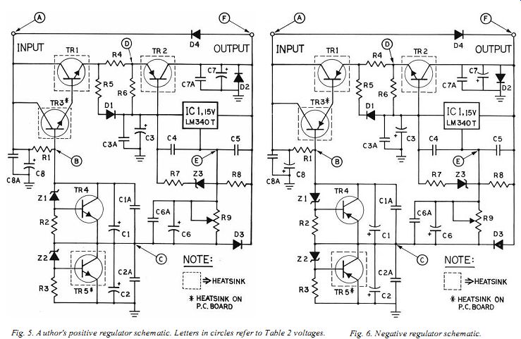
Fig. 5. Author's positive regulator schematic. Letters in circles refer
to Table 2 voltages.
Fig. 6. Negative regulator schematic.
AMPLIFIER PROTECTION
The regulator protection circuits can also protect the output transistors in the amplifier if you choose the current limit correctly. The TIP 35 and 36 transistors which Old Colony offer for the Williamson amp are rated at 25 amps and 90 watts. Into an output short, with a 68 volt supply, each transistor will see a half-cycle of 32 volts at L (the regulator short circuited current). The RMS dissipation will thus be 16 x 1 sc (which is about an amp for the 4-amp option), or about 16 watts. The full load current of 4 amps is thus only available for sine wave signals which draw less than 4 amps peak.
As the 40/40 features its own internal current limit, which would presumably act before the 4 amp sup ply limit was reached, the supply's protection is a backup. The supply's thermal protection still extends to the amplifier if the heatsinks are chosen correctly, however. I discuss the correct values below under Construction Details.
Although the 4 amp supply has a transient capability of nearly 6 amps, a pair of 40 watt stereo amplifiers ...
Table 1
... could potentially draw peak currents of 8 amps. If you intend to power both channels of your amp from a single supply, you must provide for these peaks. Using the values of R4, R5 , TR1 , and TRZ from the Pass con figuration (Fig. 5 and the parts list), we can provide up to 10 amps. Note the value of Isc goes up to about 2 amps with the higher power option, and the foldback point is also much higher; the regulator thus does not af ford the same degree of protection as if a supply were provided for each channel.
For the 80W 541 supply, we provide a 12A transient peak, or 8A
Parts List
POWERING WILLIAMSON'S 40/40 AMP:
CAPACITOR MULTIPLIER VS. REGULATOR
WHAT CHANGES CAN WE EXPECT in performance on a 40/40 if we add Reg's capacitance multiplier to the raw supply? What additional benefits are to be gained with a fully regulated supply? The table below details the results, on my own test bench, using the three options available. The capacitance multiplier adds significant filtering, which reduces the noise level at idle. This circuit also provides decoupling, which helps to reduce intermodulation distortion at high levels. In fact, the distortion performance of the fully regulated version is only slightly better than the capacitance multiplier. The full-load power capability of the regulator is much higher, however. This reflects its ability to deliver 4 amperes RMS at 68 volts. The capacitance multiplier supply had dropped to 56V at full load, which was only 2.2A RMS into 8 ohms. Into 4 ohms, the regulator was current limited at 4.5A RMS, while the capacitance-multiplier sank to 48V and 3.5A RMS. These changes result in the figures below:
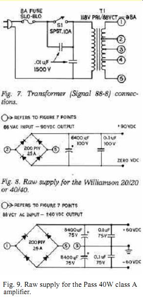
Fig. 9. Raw supply for the Pass 40W class A amplifier.
Table 2
RMS, at ±40V. Construction details for this version of the supply will ac company the power amp construction article.
The ±32 volt supplies shown for the Pass amp are optimized for the demands for the class A amp. With the recommended resistors and heat sinks, the Pass configuration will provide 15 amps for a fraction of a second (transient peaks), dropping to about 10 amps after a second or so.
The regulator thus allows for electrostatic or other reactive loads while providing protection from substantial high-power damage. This circuit's operation depends on thermal capacitance in various components, and thus the wattage rating of R, and R5 is important to correct operation ( see box on Thermal Capacitance, below).
CONSTRUCTING THE RAW SUPPLY
The raw supply feeding the regulator can be any DC supply which gives the desired full-load current and stays within the input voltage limits of Figs. 5 and 6. I think the raw supply described in Pass's article is an admirable choice. We will use a slightly different arrangement than that shown in his article, however, as we must provide a margin to allow regulation and also allow for low line voltage, component variation, and other variables.
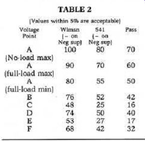
Connect the secondaries as shown in Fig. 7. If the voltage across the transformer is close to zero, reverse the secondary connections; you should get about 90VAC. To develop the raw supply of 90VDC for the 68V supply, we need about 66VAC, which we obtain from the signal 88-8 as shown in Fig. 7. Fig. 8 shows one sup ply arrangement. Note that the ripple rejection of the regulator is in excess of 120dB; thus a large ripple voltage can be tolerated as long as the minimum voltage exceeds the minimum input shown in Figs. 5 and 6.
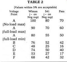
The 88VCT available using the juncture of the secondaries as a centertap is about right to provide the 60VDC no-load, 50VDC full-load capability we need for the Pass sup ply. For this application, use the con figuration of Fig. 9.
SELECTING COMPONENTS
Most parts for the supply are the same no matter what voltage and current you desire; Fig. 6, the negative supply, shows values for a negative bi-polar supply, as required for the Pass amplifier.
As shown in the construction details, the board is designed to be mounted right on the heatsink. This will keep the lead lengths to a minimum, which is important to improve transient response. Arrange things so the regulator is mounted quite close to the transistor TR2, so good thermal conduction occurs; this will ensure that the regulator can protect the transistor from overheating.
TESTING THE SUPPLY
Test each section of the supply before going on to the next section. The pre regulator section is really a completely independent regulator, with fairly good characteristics. If it tests out, we know the zener references Z, and Z2 and the IC overvoltage protection circuits are working correctly. Next we verify the IC voltage. We then test the IC foldback current limit. The final test is a "go/no-go" test of the complete regulator.
To test the pre-regulator, mount all the components except TR2 and IC,.
With voltage applied, you should be able to read the voltages shown in Fig. 5 ( or Fig. 6 for a negative supply) at the zener Z,, Z2 , and at the emitter of TR,. If possible, verify that this voltage is constant as long as the in put voltage is between the minimum and maximum values shown. Now test the overvoltage protection by shorting the cathode of D, (this is also the regulator output) to ground. Do this only if the IC and TRz are not in stalled! The voltage at the emitter of TR, should drop immediately to about 25 volts. This test must be passed for the overload circuit to function.
Next install IC,. You should be able to power up the regulator and measure all the voltage levels on Figs. 5 or 6. You should also be able to adjust the voltage around the nominal value by several volts. Now you are ready to test the overload circuit. To perform this test, you will need a 10 ohm, 10 watt resistor and either a 22 ohm, 10 watt (for the 32 volt circuit) or a 50 ohm, 10 watt (for the 68 volt circuit). Some components will get hot during this test, so perform it quickly and be careful not to burn yourself on the resistors.
After mounting the IC and TR, on a heatsink, power up the regulator and place a voltmeter across the output.
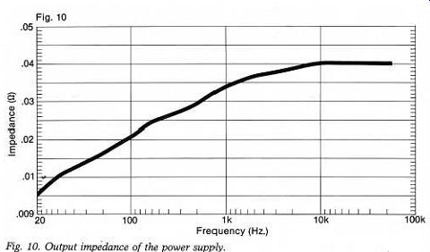
Fig. 10
Adjust the regulated voltage to the desired output level. Now place the higher valued resistor (22 ohm for the 32 volt version, 50 ohm for the 68 volts) between the output and ground.
The voltage should remain constant indefinitely. If the regulator will not supply this load, it does not have enough output current capability to work in this circuit, and you must try another IC. If the IC can deliver this current without dropping more than a fraction of a volt, then place the 10 ohm resistor across the output. The voltage should immediately drop to a low value.
Now mount TRz and install every thing back on the heatsink. Unless you have some very large resistors on hand, this is all the testing you can perform (the supply can deliver over 300 watts). Check the output to be sure that it is still in regulation by varying the output voltage with the trimmer pot.
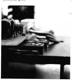
Fig. 14. Closeup of one of the author's early prototypes showing the board mounted on standoffs to a flat-sided heatsink. Three of the power devices, TR,, TR2, and IC, are mounted in such a way that their leads are soldered to the board, bent at right angles and then mounted on the heat sink with insulating hardware and thermal grease.
-----------
THERMAL CAPACITANCE
The regulator design takes advantage of the heatsink's thermal capacitance to provide a transient peak current capability about 50 percent higher than the RMS maximum. Thermal capacitance is really a measure of a component's ability to remain cool despite a heat input exceeding the device's heat output capability. For example, when the Pass amp delivers the 15 amp peak currents shown in his article (Figs. 22a and 22b, TAA 4/78, p. 11), the RMS value of the power required is small. When the regulator is cool (i.e., no signal), R, maintains its nominal value and the peak available current is 6.6 times the maximum LM340T current. The LM340T can deliver more than 2 amps in this configuration, if the junction is cooler than about 500C.
Thus the maximum transient current for a cool regulator is 6.6 x 2 or nearly 14A. If this current is maintained for more than a fraction of a second, however, the 12 amp current through R, (which develops more than 14 watts) rapidly heats the ni chrome of which the resistor is made, and as it has a strong coefficient of resistance vs. temperature, its resistance rises also. This reduces the maximum current available.
At the same time, the LM340T is heating. At 850C the maximum available current is reduced to 1.5 amps. This results in an equilibrium point with total current available at about 10 amps. R, is dissipating about 5 watts, the LM340T is at or below 850C, and stability is achieved. The regulator can thus supply 10 amps steady-state, or a recurring peak transient of over 14 amps.
------------------
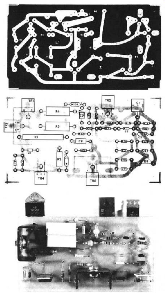
Fig. 11. Full sized negative of the author's circuit board. Fig. 12, center is a stuffing guide for the circuit card. Fig. 13, bottom, is a photo of the author's board. The on-board heatsinks have solderable tabs for attaching to the board. The three devices at the top attach to a flat sided heat sink, as does the board itself.
A NOTE ON WIRING
The regulator senses voltage at the IC's output terminal. The wiring from this point to the amplifier should be substantial to avoid degrading the regulator response.
The output impedance is only 0.05 ohm; this much resistance can be found in only a few feet of #18 wire.
To keep performance up, use #14 wire and keep the lead lengths short. Also, return the speaker leads right to the ground of the raw supply rather than to the amp or regulators, to eliminate ground return IR losses.
The best approach is to mount the regulator and its heatsink right next to the power amp, arranging things so that the least possible lead length is required to bridge the gap. The leads going to the regulator are not as critical, and can be long without problems. The output impedance can be reduced, especially at high frequencies, by adding a capacitor from output to ground (i.e. in parallel with C,). This will also give the regulator the ability to withstand a dead short more easily, by increasing the risetime of the overload current waveform. This can be a two-edged sword, however, as the same increase shows up in the fall time of the output voltage. The load must therefore be able to withstand a longer and larger overload pulse. Among the amps we are considering, the only one which might have a need for the fast limiting is the original 20-20. All the rest are self-protecting to one extent or another. If you figure about 1000uF per RMS amp of load current, you should be on safe ground.
For best results, place this cap across the supply as close to the power amp as possible. This value of cap will flatten the impedance curve at about the 100Hz value, or about 0.02 ohms.
The supply will provide thermal protection to the amp if the regulator and amp share a common heatsink, as long as the overload points are those suggested in the article. If the regulator is added to an existing amp, thermal protection can still be provided, as long as the heatsinks on the supply are no more than half as large as those on the amp (i.e. twice the thermal resistance in C/W). This assumes a physical placement where the airflow for all sinks is similar.
FOR THOSE WITH OTHER POWER NEEDS
You can easily scale the output voltage by changing the value of Z2 and the capacitor C2 The maximum output voltage with the transistors shown is about 80 volts (from a Z2 value of about 65 volts).
Output currents in excess of the 10 amps (RMS) maximum can be obtain ed by using a pair of 0.1 ohm resistors in parallel to improve the wattage rating and reduce the resistance. You must also increase the transistors TR1 and TR2 to avoid the danger of secondary breakdown on an overload.
A FINAL CAUTION
This supply will source a tremendous amount of power. It is designed to drive an active load, not a crowbar. It may survive a dead short across the supply output; but then again, it may not.
The overload response is improved if an additional output cap is added as described above. If you intend to short the supply (as you might on a bench supply be sure to add this cap.
Remember that this protects the supply, but reduces load protection.
Also see:
Are Those Ears Really Golden? (Or only Iron Pyrites?) -- Extensive explorations of whether listeners detect differences in equipment, by Thomas H. Smith, Michael R. Peterson and Peter O. Jackson
A High Accuracy Inverse RIAA Network -- New light and hardware for the phono curve's basic shape, by Stanley P. Lipshitz and Walt Jung