THE BORBELY PREAMP: PART 1
DESIGNING A PREAMP is probably the most challenging engineering task in the audio chain, and many designers have invested a lot of time and effort in it. We have come a long way from the two-transistor RIAA and line amplifiers typical of the late sixties to today's sophisticated discrete and monolithic operational amplifiers. Nevertheless, the subject still elicits lively discussion in hi-fi magazines (including TAA).
The controversy includes varying opinions on topics such as tube versus transistor sound, op amp versus discrete design, feedback versus no feedback, tone controls and regulated supplies. These discussions can be come quite emotional, lacking the necessary scientific reasoning. But if everything could be explained scientifically, I probably would not be writing about yet another preamp design.
Why Another Preamp?
My reason for designing this preamp (Photo 1) is quite simple: I wanted to have a top-quality preamp without paying megabucks for a Levinson or Accuphase unit. It is up to you to decide whether or not I have succeeded in achieving the same quality.
These were my design goals and decisions:
1. Input switching. My hi-fi set up at home is fairly simple. I use one turntable, a compact disk player and one tuner in my permanent installation. Occasionally, I add a tape ma chine to this. Consequently, one phono input, two line inputs and a tape monitor input are all I need in a preamp. This should not, however, prevent you from adding several more inputs and tape features if you need them.
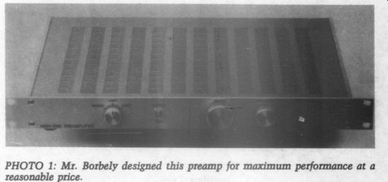
PHOTO 1: Mr. Borbely designed this preamp for maximum performance at a reasonable price.
2. Tone controls. I never use tone controls because they usually do not provide the required frequency range and boost/cut. Theoretically, I am not against tone controls, and if there is sufficient interest, I will be more than happy to suggest a professional one.
3. Circuit design. If I am a minimalist in terms of switching and other features, it certainly does not apply to circuit design. The circuitry is the heart of the amplifier, and I try to avoid compromises there. One important decision based on this philosophy was to use discrete circuitry in stead of the more convenient integrated circuit (IC) op amps. I believe that a well-designed discrete amplifier produces better sound than one with op amps. I have drawn freely on previous experience (mine and others) in the audio field and in other electronics disciplines, notably instrumentation. I hope I have given credit where it is due.
4. Mechanical components. Al though not claiming to hear a difference between silver and gold contacts, I prefer the gold ones because of reliability. I want my preamp to work and sound the same three years from now, and I think only gold plated connectors and switches guarantee this.
RIAA Design Considerations The two most important considerations when designing RIAA amps are dynamic range and RIAA accuracy.
The dynamic range is limited on one side by the maximum input level it can accept without overloading the amplifier. The other limiting factor is the input noise of the RIAA stage.
The range of input signals we can amplify lies between these two limits. Optimizing the dynamic range of an RIAA amplifier (or any amplifier, for that matter) means getting as much overload capability and as low noise as possible.
Generally, you can increase the overload margin or upper limit by two means: operating the amplifier at very high supply voltages and keeping the gain as low as possible. When using IC op amps, the supply rails are automatically limited to approximately +/- 57 because this is the maximum voltage the IC can handle.
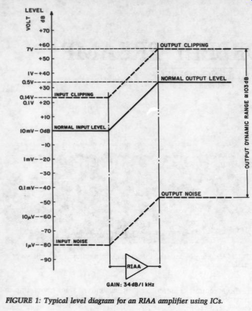
FIGURE 1: Typical level diagram for an RIAA amplifier using ICs.
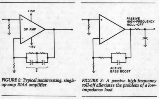
FIGURE 2: Typical noninverting, single op-amp RIAA amplifier.
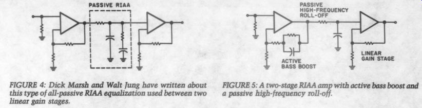
FIGURE 3: A passive freq. roll-off affects low impedance load.
This limits the maximum output swing to around 7V RMS. Discrete designs have practically no supply voltage limit. Indeed, some manufacturers use +45V and +90V on the RIAA amp.! Tube preamps use even v higher voltages.
We cannot do much about the gain because it is dictated by the sensitivity of the cartridge used. For moving magnet cartridges, 34dB (or 50 times) seems to be a standard. This will pro duce a 0.5V output with a 10mV in put. Assuming an IC-based RIAA amp with a maximum output of 7V RMS, he amp will accept an input voltage of 140mV maximum, which corresponds to an overload margin of 23dB. Figure 1 shows a level diagram or such an amplifier. With an input noise of pir 1uV, which is Sp. or op amps, you will have a dynamic range of 103dB for this RIAA at.
Up to now, I have considered signal levels at only 1kHz. Due to the RIAA characteristics, the gain varies considerably at different frequencies.
Compared to 1kHz, the gain at 20Hz is almost 20dB higher, and at 20kHz it is approximately 20dB lower. Again assuming a 1kHz gain of 34dB, we have to cope with a gain range of 14 to 54dB through the audio band. At 20Hz, where the gain is 54dB (or 500 times), the IC amp will accept only 7V/500, which equals 14mV; at 20kHz, where the gain drops to 14dB (5 times), the input overload is 1.4V.
These numbers are based on the non inverting, single-op-amp RIAA stages most often used in preamps (Fig. 2).
They are also theoretical numbers.
Practical circuits with different op amps and feedback circuits might offer slightly better or slightly worse specifications.
The single-stage RIAA amp shown in Fig. 2 has several disadvantages.
The feedback network, which pro vides the RIAA correction, has a varying impedance with frequency. This impedance is lowest at high frequencies, which puts a very heavy load on the amp in the 10 to 20kHz range.
Also, because the configuration is noninverting, the gain will flatten out at 1 (or 0dB) even if you reduce the impedance of the feedback network to zero. This tends to give an equalization error around 20kHz.
We have another problem at low frequencies, where the gain is very high, flattening out at around 54dB below 20Hz. To avoid equalization error, the open-loop gain of the amplifier must be significantly higher than the 54dB closed-loop gain.
Traditionally, this was the biggest problem with early transistor RIAA amplifiers. With today's high-gain op amps, this problem is significantly reduced.
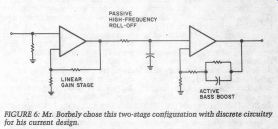
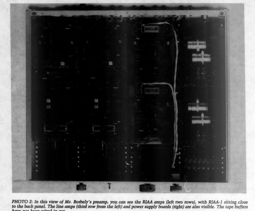
Photo 2.
[...] general and FET input stages in particular, so I wanted to replace the bipolar input transistors with JFETS, as shown in Fig. 8. As a matter of history, I tried to do this back in 1980, but could not find good enough complementary JFETs at that time.
(That search resulted in the adaptation of the AH50xx P-channel JFETs in my designs, but as I described in my article in TAA 5/83, p. 7, they were not good enough for low-noise applications.) In 1981, I learned about the low-noise complementary JFET family from Toshiba, but it took me more than two years to get the first samples. The FETs in question are the 2SK147 N-channel and the 2SJ72 P-channel devices.
Apparently developed for low-noise audio applications, these FETs have a very high transconductance (gm).
Typically, gm equals 40mmbho at a drain current of 5SmA. This is significantly higher than “normal ” JFETs.
The 2N5565, which I am sure you know from previous TAA designs, has a typical gm of about 10mmbho at the same drain current. Since the equivalent input noise is inversely proportional to gm, it is quite natural to expect very low input noise with these FETs. Indeed, the 2SK147 has an input noise of 0.75nV/ Hz at a drain current of 2mA, which is equivalent to the thermal noise of a 35 ohm resistor. This compares quite favorably even to a low-noise bipolar transistor such as the LM394, which has an equivalent spreading base resistance of 40 ohm.
Unfortunately, you do not get anything for nothing, and in this case, you have to pay with a fairly high gate-to-source capacitance (Cgs).
Cgs equals 60pF for the 2SK147 and 130pF for the 2SjJ72. Worse yet, the feedback capacitance is also quite high-15pF for the N-channel and 55pF for the P-channel. When used in a normal common-source circuit, these FETs have a very high input capacitance because of the Miller effect. (The phenomenon by which an effective feedback path between the input and output of an electronic device is provided by the capacitance between specified electrodes. This can affect the total input impedance, which results in the total dynamic in put capacitance being always equal to or greater than the sum of the static electrode capacitances.) You must
[...]
------------------
PARTS LIST THE FIRST STAGE (RIAA-1)
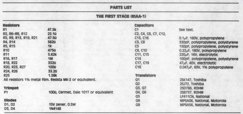
Resistors R1 47.5k R2, R6-R8, R12 2210 R3, RY, R13, R19, R21 47.50 R4, R14 5620 RS, R15 1K R10 4750 R11 5.62k R16, R17 Mm R18, R22 3320 R20, R23, R27 1000 R24, R26 33.20 R25 1.58k
Capacitors C1 See text.
C2, C4, C6, C7, C12, C13, C16 C3, C8 CS C9, C10 C11, C15 cia C17, C19 c18
Transistors
All resistors 1% metal film. Resista MK-2 or equivalent. 1 1000, Cermet, Dale 101T or equivalent 15V zener, 0.5W 1N4148 Q2 Q3, Q7 Q4, Q6 Qs Q8 Q9
0.1uF, 160V, polypropylene 330pF, polypropylene, polystyrene 150pF, polypropylene, polystyrene
0.22uF, 160V, polypropylene 220 uF, 16V, electrolytic 100pF, polypropylene, polystyrene 47uF, 40V, electrolytic
0.047uF, 63V, 1% polypropylene 25K147, Toshiba 25J72, Toshiba 25D786, ROHM 2SB737, ROHM LF411CN, National MPSAD6, National, Motorola MPSAS6, National, Motorola
------------------
... take special precautions to avoid this in the final circuit.
The simplified bipolar circuit in Fig. 7 does not show the necessary biasing for the input transistors. If you use JFETs that are normally “on, ” theoretically no biasing is needed. In a practical amplifier, how ever, you must reduce the rather large variation of Ipss (saturation drain current measured with Vgs = 0). In the case of the 2SK147/28])72, Ipss equals 5 to 30mA.
The FETs are available in three Ipss groups from Toshiba: GR:5 10mA, BL:8-16mA and V:14-30mA.
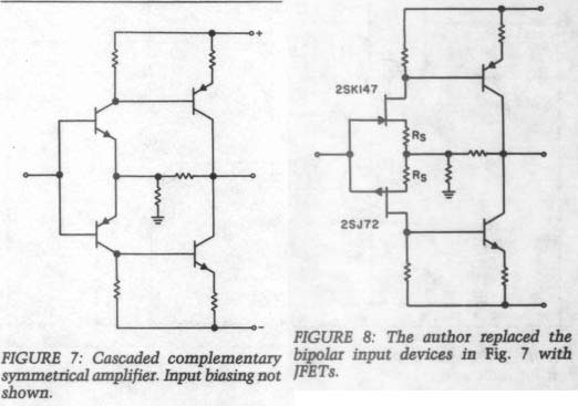
FIGURE 7: Cascaded complementary symmetrical amplifier. Input biasing
not shown.
For optimum noise in this application, the FETs should be operated at Ip (actual drain current) greater than 2mA (Fig. 9). I have chosen to operate them at around 5mA, which further improves noise performance and also increases gm. To stabilize the drain current at 5SmA, I inserted a resistor (Rs) in the source, as shown in Fig.
8. To select this resistor, you must look at the Ip-Vps (drain-source voltage) characteristics. Figure 10 shows typical characteristics for the 2SK147. You can read the gate-source voltage (Vgs) off this figure: for an Ip of 5mA, you need a Vgs of approximately 0.1V. Therefore, Rs will be determined as follows:
Ideally, the N and P-channel FETs should come from the same Ipss group, and if possible, only the lowest two Ipss groups should be used. (Old Colony will offer them in pairs like that.) If you get different Ipss groups, you can still use them, but make some measurements to ensure proper operation. When supply voltage is applied, measure the voltage drop across the drain resistors. It should be about 2.8V. If it is more than 20 percent off (less than 2.2V or more than 3.3V), you must adjust the source resistors.
When the voltage drop is too high, in crease the source resistors; when it is too low, decrease them. Unfortunate ly, I cannot give you the correct Rs values for all combinations of Ipss, so you must do some experimenting yourself. If this is beyond your re sources, I suggest you buy this module fully assembled and tested from Old Colony.
Figure 11 shows the complete schematic of the input stage. Because the FETs have negligible gate current, the cartridge is DC-connected to the input. C1 is the loading capacitor for the cartridge and should be selected according to the manufacturer's specifications. The amplifier's input capacitance is approximately 60pF, which should be deducted from the 2SKi47 FIGURE 8: The author replaced the bipolar input devices in Fig. 7 with J-FETSs.
FIGURE 9: The 2SK147 has a very low equivalent input noise for an Ip greater than 2mA.
recommended value. You may solder C1 on the board. EE the input stage, cascoded by Q3 and Q4.
I have three reasons for using a quality film capacitor in cascoded input stage. First operated at less than a 15V drain source voltage, according to the Toshiba data sheet. By biasing the cascode stage at 15V, the drain-source voltage will be limited to approximately 14.4V. Second, as mentioned before, the FETs have a very high in put capacitance because of the Miller effect. Using a cascode configuration reduces this significantly. Finally, the cascode configuration is inherently more linear than the single, common-source stage. You need a + 15V supply for the servo amplifier any way, so adding the cascode is easy.
The 15V bias voltage is taken directly from the 15V zeners.
The second stage of the amplifier consists of Q6 and Q7, which are nor mal common-emitter stages with partially decoupled emitter resistors. R19 and R21 introduce local feedback to improve linearity. Connect a high […] parallel with the electrolytic decoupling capacitor.
First, for optimum noise, the FETs should be
Q6 and Q7 (and Q3/Q4) are special.
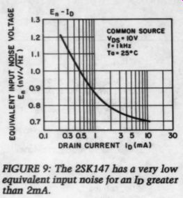
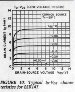
FIGURE 10: Typical Ip-Vps characteristics for 2SK147.
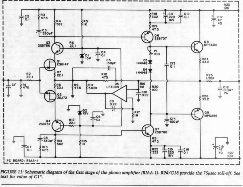
FIGURE 11: Schematic diagram of the first stage of the phono amplifier (RIAA-1). R24/C18 provide the 75 usec roll-off. See text for value of C1.
... low-noise transistors from ROHM.
Best known on the market for the lowest spreading base resistance, they offer extremely low noise with very low source impedances. Consequently, they are often used in pre-pre-amps. Other transistors could do the job from the overall noise point of view, but none offers the low flicker noise and the same linearity. One of the more important features of the preamp described here is the excellent low-level resolution. I at tribute this, at least partially, to the input FETs and the ROHM low-noise transistors.
The output stage is an emitter follower, using the widely known MPSA06/MPSA56 general-purpose bipolar transistors. The bias network consists of P1, D3, D4 and R20. P1 is used to adjust the quiescent current by measuring the voltage across the two emitter resistors. Set it to 1V, which corresponds to approximately 15mA. Put a small snap-on heatsink on these devices, as they tend to be hot. The layout is such that you can use other devices, including the Hitachi 25K216/2Sj79 MOSFETs. In this case, you can experiment with the quiescent current to get the best sound. You do not need D3 and D4 with the MOSFETs, and you should change P1 to 5000 to get the necessary adjustment range.
Feedback resistors R9 and R10 set the gain of the first stage to approximately 11 times (20.8dB). I selected resistor values to produce as low noise as possible with the given drive capability of the output stage.
R25 and C18 provide the 75-usec roll-off for the RIAA equalization. In selecting the value of R25, take into account the output impedance of the first stage and the input impedance of the second stage. R25 should be a 1 percent metal film resistor and C18 a 1 percent polypropylene or poly styrene capacitor.
The servo amplifier is an LF411 BIFET op amp. I selected R16/C10 and R17/C9 to give a -3dB of less than 1Hz. The output of the servo ...
-----------------
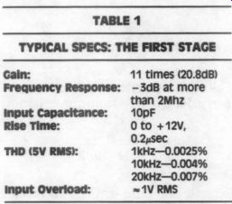
TABLE 1
(20.8dB) Frequency Response: -3dB at more than 2Mhz Input Capacitance: 10pF Rise Time: 0to +12v,
0.2usec 1kHz-0.0025% 10kHz-0.004% 20kHz-0.007%
=1V RMS
----------------------
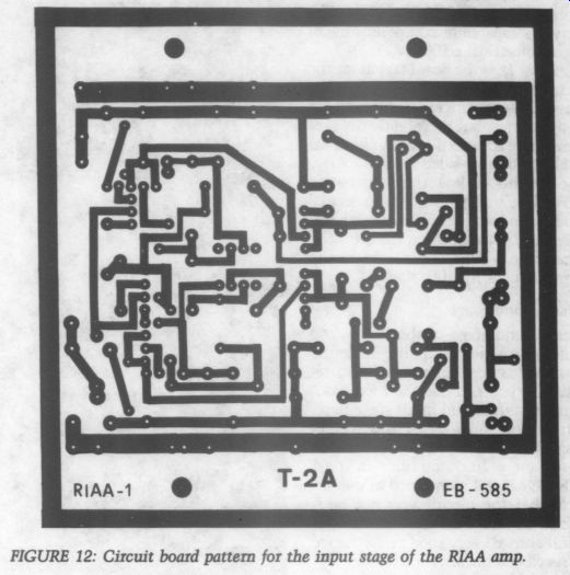
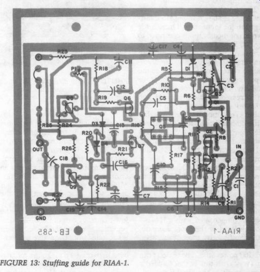
FIGURE 13: Stuffing guide for RIAA-1.
... ed audiophiles making double-sided boards. Also, the layouts follow the schematics very closely. This makes it easier to understand and troubleshoot them.
a BB EL a first stage, while Table 1 shows the typical specs for this stage.
The Second Stage
The second stage of the RIAA amp (Photo 3) is not as critical in terms of noise as the input stage. Consequently, you can use the more con As for the topology of the second stage, | have chosen the same as I pro posed for a line amplifier in TAA 5/83 (Fig. 14). I mentioned in that article that the circuit was not optimized for one particular application, but it showed very good performance in speed and linearity. I have now optimized it for the second stage of the RIAA amp and my line amp.
The complete schematic of the second stage is shown in Fig. 15. Starting with the input stage, I have made Fig. 14. First, I added a cascode stage for basically the same reasons as in the input stage: to limit the drain source voltage to 15V, to reduce the input capacitance and to improve linearity. The second modification is an increased drain current: Q1 and Q2 work at 5mA per FET to reduce noise. This modification, together with on-board regulators, improved the input noise by more than 6dB compared to the original circuit.
I wanted to use the LM334Z cur rent sources instead of the discrete ones consisting of Q7/Q8 and associated circuitry, but the LM334Z cannot handle the power dissipation and the 24V supply voltage. The current sources shown have a partial temperature compensation: the transistor's VBE is compensated with a 1N4148 diode instead of the more accurate, but significantly more expensive, dual-transistor approach I used in the DC-100 power amp. The reason I can get away with this is that I added a servo circuit to the amplifier.
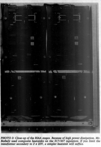
PHOTO 3: Close-up of the RIAA stages. Because of high power dissipation,
Mr. Borbely used composite heatsinks on the 317/337 regulators. If you
limit the transformer secondary to 2 x 22V, a simpler heatsink will suffice.
The second stage of the amplifier is the same as in the original, except for the bias circuit. As in the input stage, I rely on a potentiometer to ad just the bias instead of the Vg multiplier circuit. The output stage is an emitter follower using MPSA06/ MPSAS56 transistors. The layout is again such that you can add the Hitachi MOSFETs.
R20, R22, R23 and Cf make up the low-frequency part of the RIAA compensation. Because the 75usec roll-off is separated from the active compensation, it is easy to calculate this feed back network.? To make the calculation easier to understand, the low frequency part of the RIAA frequency response is shown in Fig. 16. The resistor designations are the same as the ones in Fig. 15.
The f1 = 50Hz breakpoint is given by the equation Ce 2x (R20) (Cf) Selecting a practical value for Cf, you can calculate R20 from the equation 1 R20 = ns 2x (50) (Cf) Because the ratio of the two break--points (500Hz and 50Hz) is 10, the ratio of the two gains (Apc/Anr) is also 10. If the gain at low frequencies (Apc) is given, you can calculate R22 from the equation R22 = 10R20) 9(Apc) Finally, you can calculate R23 from the equation R23 = 20 - R22 Note that the only assumption in this calculation concerns the open loop gain, which must be significantly higher than Apc. This requirement is very simple to satisfy in the two stage RIAA circuit, and the RIAA correction will be accurate. Naturally, the above calculation also applies to other discrete and monolithic op amps.
---------------
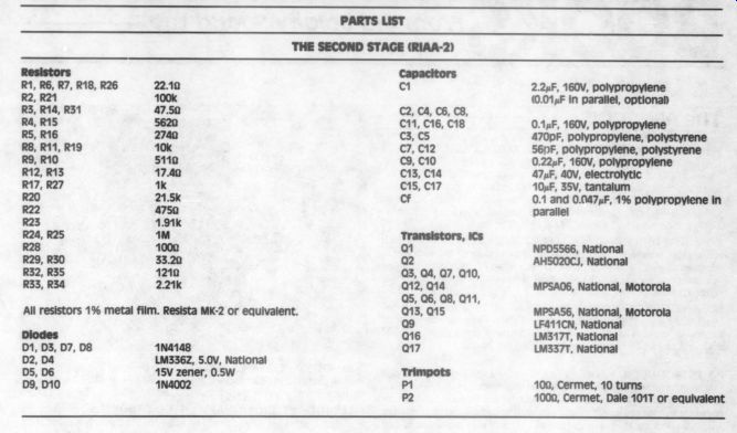
THE SECOND STAGE (RIAA-2)
------------ -----------------
Resistors R1, R6, R7, R18, R26 2210 R2, R21 100k R3, R14, R31 47.50 R4, R15 5620 RS, R16 2740 R8, R11, R19 10k R9, R10 5110 R12, R13 17.40 R17, R27 1k R20 21.5k R22 4750 R23 1.91K R24, R25 mm R28 1000 R29, R30 33.20 R32, R35 1210 R33, R34 2.21k All resistors 1% metal film. Resista MK-2 or equivalent.
D1, D3, D7, D8 1N4148 Capacitors (oy C2, C4, C6, C8, C11, C16, C18 C3, C5 C7, C12 C9, C10 C13, C14 C15, C17 Cf Transistors, ICs (a 1} Q2 Q3, Q4, Q7, Q10, Q12, 14 Q5, Q6, 08, Q11, Q13, 15 Q9 Q16 Q17 D2, D4 LM336Z, 5.0v, National D5, D6 15V zener, 0.5W D9, D10 1N4002 Trimpots m1 P2 2.2uF, 160V, polypropylene (0.01uF in parallel, optional)
0.1uF, 160V, polypropylene 470pF, polypropylene, polystyrene 56pF, polypropylene, polystyrene
0.22uF, 160V, polypropylene 47uF, 40V, electrolytic 10uF, 35V, tantalum
0.1 and 0.047uF, 1% polypropylene in parallel NPD5566, National AH5020C)J, National MPSA06, National, Motorola MPSAS6, National, Motorola LF411CN, National LM317T, National LM337T, National 100, Cermet, 10 turns 1000, Cermet, Dale 101T or equivalent
------------------
Let's go through the calculation of the network I used. In selecting the capacitor Cf, you must consider the overall impedance of the feedback network. For low noise, the impedance should be as low as possible.
There is, however, a limit to how low you can go because the amplifier has to be able to drive it. Also, the lower the impedance of the network, the ...
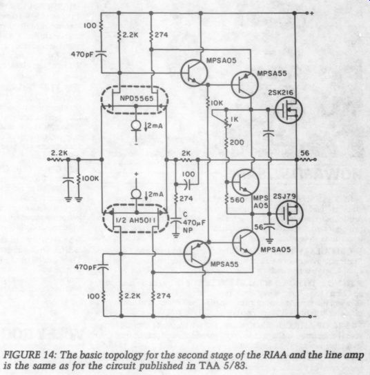
FIGURE 14: The basic topology for the second stage of the RIAA and the line amp is the same as for the circuit published in TAA 5/83.
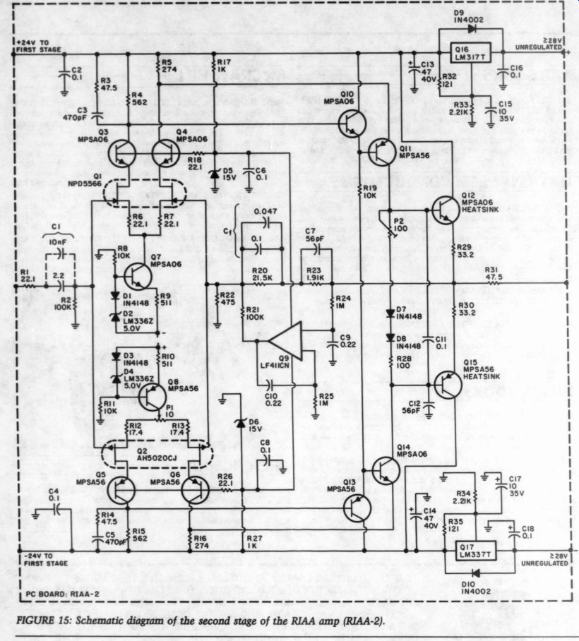
FIGURE 15: Schematic diagram of the second stage of the RIAA amp (RIAA-2).
... larger the value of the capacitor. 1 wanted to use precision polypropylene or polystyrene capacitors, so I had to look at what was available on the market with, say, 1 percent tolerance. Values up to 0.1uF are easy to find, but higher values normally re quire paralleling of smaller ones.
I calculated the feedback network for capacitor values between 0.1uF and 0.33uF, finally settling on 0.147uF, which is 0.1 in parallel with 0.047. (I also used 0.047 for the 75usec roll-off in the first stage.) R20 can be found with the equation R20 = 1 2(50)[0.147uF) ~A-65K0
The closest value in 1 percent metal film is 21.5 k-ohm , so I used this in the amplifier.
To be able to calculate R22, you must know the gain at very low frequencies. If you select a total gain of 344dB for the RIAA amplifier and the first-stage gain is 20dB as shown earlier, then the second-stage gain has to be 14dB (or 5 times) above 1kHz (Aur). Apc is equal to 10 times Aur (Fig. 14), so it must be 34dB [or 50 times). You can now calculate R22 from the equation
_ 10(R20) _ 10(21.5k) 9(Aoc) 9(50) R22 = 4770
The closest 1 percent value is 4750.
R23 is then given by the equation R23 =R20_pop 25K _ 475.1910
This completes the calculation of the feedback network. Measurements using the Lipshitz/Jung inverse RIAA network' show no measurable error in the RIAA compensation. If you have access to a stable audio oscillator and an inverse RIAA network, I suggest you check your circuit as well.
Continuing now with the description of the second stage, you will notice that I have an offset adjustment in the first stage (P1) and a ser vo amplifier. This is a bit of overkill:
you do not really have to adjust the offset if you have a servo, but I prefer doing that just to know what the initial offset is. Also, while I cannot get rid of the servo (FETs have a significantly worse temperature behavior than bipolars), I want it to track temperature drift only, not initial off set. (The same arguments could also be applied to the first stage, but I did not want to put a trimpot there for noise and distortion reasons. Remember the extremely low-level signals we are amplifying in that stage.) Proper setup procedure, in case you choose to use both, is to adjust the output offset to zero before inserting Q9. If you do not use P1 (R12/R13 are then 22 ohm each), simply insert Q9, and it will take care of the offset. P1 should be a cermet trimpot for low noise and good stability.
Q16/Q17 and associated components provide regulated + 24V to the second stage of the RIAA amp and, through a further RC filter, approximately +22V to the first stage. I chose the LM317/LM337 three-terminal regulators for these functions.
I recommend all three capacitors shown in connection with the regulators: C16/C18 for stability reasons, C15/C17 to improve ripple rejection and output impedance, and C13/C14 to improve load transient response.
---------------
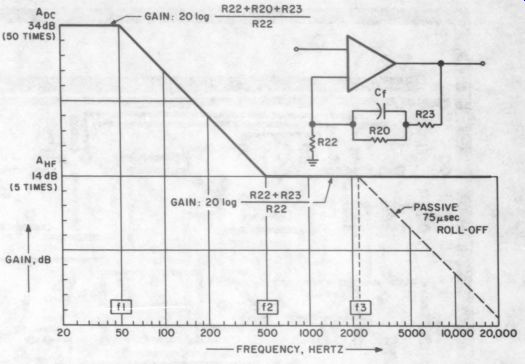
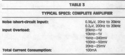
TABLE :
Frequency Response:
Capacitance:
Time:
HD (10V RMS):
5 times (14dB)
-3dB at 1.4MHz 10pF 30V p-p, 0.3 usec 1kHz-0.0025% 10kHz-0.0045% 20kHz-0.007%
------------------
2/C4 are high-quality film caps, helping to improve high-frequency decoupling. In case of accidental shorting of the input to the regulators, output capacitors C13/ 14 will discharge into the output of he regulators. When C13/C14 are larger than 25uF, this discharge can cause damage to the regulators.
Diodes D9/D10 prevent this damage.
The regulators should be mounted with a heatsink, with thermal resistance of approximately 20°C/watt. I used a heatsink that can be soldered to the board, but you can adapt other heatsinks easily.
Although the LM317/LM337 regulators have quite low output impedance up to 100kHz (less than 0.20), there has been some discussion in TAA that this is not good enough for preamps. Without taking sides, I suggest that you make your own decision: if you think that you might gain in sonic quality by using a discrete regulator, do not hesitate to design one. You can simply leave out the regulators when you assemble the board and connect the supply lines to your own regulator.
Figure 17 is the board layout for the second stage of the RIAA amplifier, and Fig. 18 is the stuffing guide. I used gold-plated sockets for Q1, Q2 and Q9; the other components are soldered directly to the board. Table 2 shows the typical specs for the second stage. Table 3 shows the typical specs for the complete RIAA amplifier. Figure 19 shows the pin-outs for the devices used in my design.
---------------
FIGURE 16: Asymptotic presentation of the frequency response of the second stage, which provides the bass boost for RIAA compensation. The passive 75usec roll-off is provided by the first stage.
-------------
TABLE 3 TYPICAL SPECS: COMPLETE AMPLIFIER
Noise (short-circuit input):
input Overload:
0.36xV, 20Hz to 20kHz
0.2uV, 200Hz to 20kHz 20kHz-1V 10kHz-1V 1kHz-240mV 100Hz-50mV 20Hz-25mV 100mA
--------------------
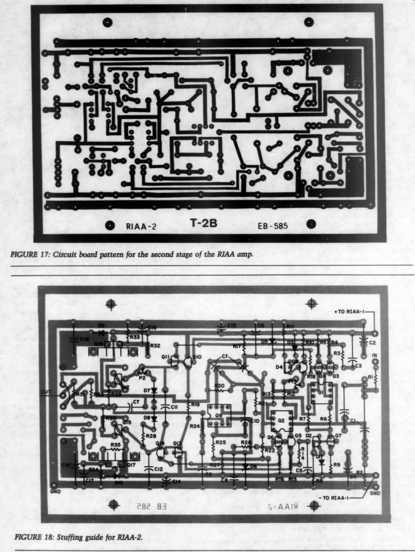
Fig 17, 18
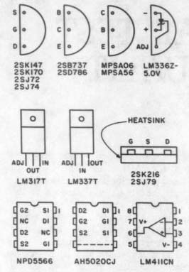
FIGURE 19: Pin-outs for the devices used in Mr. Borbely's design. These are bottom views, except for the LM317/337.
Next time, Mr. Borbely will continue with his design, adding a line amp and the power supplies.
REFERENCES
1. Perreaux SM2 preamp, Audio, July 1984.
2. Baxandall, P.J., 'Letters to the Editor,’ JAES (Volume 29, Number 1/2), January/February 1981.
3. Jung, W.G., “Topology Considerations for RIAA Phono Preamplifiers, ” Preprint 1719, 67th Convention of the AES, October 31/ November 3, 1980.
4. Jung, W.G., and S. Wurcer, “Instrumentation Amplifiers Solve Unusual Design Problems, ” EDN, August 4, 1983.
5. Tape Playback Amplifiers, ” JAES (Volume 13, Number 1), January 1968.
6. Netzer, Y., “The Design of Low-Noise Amplifiers, ” Proceedings of the IEEE (Volume 69, Number 6), June 1981.
7. Lipshitz, Stanley P. and Walt Jung, “A High Accuracy Inverse RIAA Network, ” TAA
By Erno Borbely.
----
Also see:
PREEMINENT PHONO PREAMP, By John H. Roberts