THOSE OF YOU actively involved in designing audio circuits with discrete transistors know that, beyond the selection of the circuit topology, a design's success is very much dependent on the transistors, themselves. You would think all transistors are properly characterized by their manufacturers, and the characteristics are published in datasheets or in data-books. Selecting the right transistor for a particular application should be a simple matter.
This is not always so. Although it is true (at least I hope so) that all transistors are properly characterized before going into production, only part of this characterization data is published in datasheets and data books. Most manufacturers give you typical characteristics in graphics form, and tabulate minimum and maximum values, when applicable. Some parameters, however, are only stated in the “typical” column, with no guaranteed minimum and maximum values.
I have tested a lot of transistors in the last 30 years, and can assure you that many of the characteristics and parameter data didn't look much like the published ones. This is, of course, natural: you can't include all the production tolerances and temperature variations, as well as variations caused by improvements in process technology, among other things, on a two-page datasheet.
Consequently, most end-users, the manufacturers of electronic equipment, including those in audio, run tests on the transistors prior to building them.
Testing in manufacturing can be a fairly simple affair, if it involves only a single or maybe a couple of parameters. Checking a transistor for a minimum hg value, for example, requires a simple test jig with a couple components, a meter and a power supply.
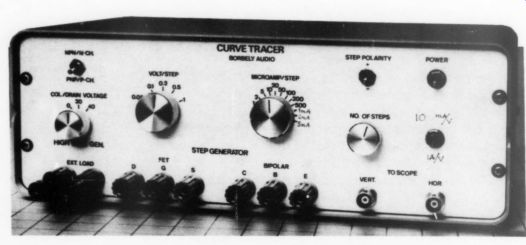
PHOTO 1: The Curve Tracer's front panel layout with one of the test-heads
plugged into the bipolar connectors.
Similarly, if you only have to determine the saturation voltage of a high voltage transistor is always below a given value, you will probably build a special test jig for the job. Even when matching transistors, you don't need very sophisticated equipment.! However, in de sign, where I select transistors for a particular job, I prefer to work with a curve tracer, allowing me to look at many parameters simultaneously, making the selection process more efficient.
To give you an idea what parameters I was looking for when I worked on the very low distortion circuits in Part III of the 'Measuring Nonlinear Distortion' (TAA, 3/90) series, I displayed the transistors' I~ vs. V; characteristics, read/ calculated the values for hg, looked at the hg; linearity (spacing be tween the lines), calculated the Early voltage from the slope of the curves, and checked saturation voltage at the collector current at which I wanted to operate the transistor. I did the same with JFETs and MOSFETs. The critical parameters were, at times, different from those of the bipolar transistors.
Naturally, you can do a lot more ...
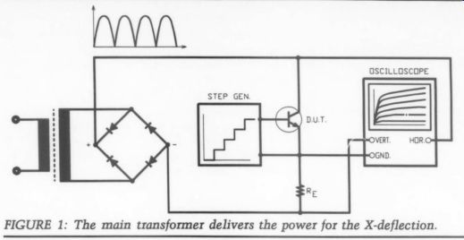
FIGURE 1: The main transformer delivers the power for the X-deflection.
... with a curve tracer. You can easily display semiconductors' input characteristics (I- vs. Vg; or I, vs. Vg) and check temperature dependence by heating or cooling the devices. A simple switching arrangement enables you to compare and match transistors. Building some simple bias circuits into your test-head allows you to display the composite characteristics of cascode connected transistors. Naturally, curve tracers are not limited to transistors: you can test small signal, reference, rectifier, and zener diodes as well. All in all, it is a very useful device when dealing with a large number of semi conductors. Unfortunately, commercial curve tracers are out of reach for most of us. Even if we have access to such machines, building a simple curve tracer adapter is worth considering.
The Step Generator
In the late 1960s and early 1970s, you could find a number of articles on curve tracer design.?" Most of these designs can be described with the simple block schematic in Fig. 1. The collector emitter voltage difference V; is swept in half- or full-wave rectified pulses (full-wave is shown here), and provides the X-deflection for the scope. Current through the transistor flows through resistor Rg, and the voltage drop across it provides the Y-deflection. Base cur rent is stepped in equal increments by a staircase, or step generator, on successive sweeps of the collector-emitter voltage, and recycles back to zero after the required number of steps.
Naturally, you can use other wave forms, such as a saw-tooth used in the scope's own deflection circuit for the Vc; deflection. In that case, however, you must generate this waveform your self. The advantage is: you can run the curve tracer at a much higher frequency, and get an almost flicker-free display. This is practically impossible with 50Hz or 60Hz. The disadvantage is: if you want to test power transistors, you will need a power amplifier for the Vcr waveform. In the circuit in Fig. 1, the main transformer delivers the power for the X-deflection, and this can easily be selected for the particular application.
The curve tracer's heart is the step generator, which provides the base cur rent to the transistor. Most of the de signs mentioned above produced a volt age step, which subsequently was turned into a current step. One of the problems with these early designs is related to this voltage-to-current con version. Most people, myself included, used a series resistor. This created a number of problems, as we will see.
You can make a simple staircase or step generator using a “diode pump” C1 D2 Vm 7] I I |
Your D1 c2 Vour (Figs. 2a, 8, 9).
Assuming both capacitors initially have zero charge, the out put voltage Vy is also zero. The first negative-going pulse will cause D1 to conduct, and assuming that Vp, is greater than Vj, C1 will be charged to Viv. The time constant by which C1 is charged is equal C1 x Rg, where Ry is the sum of source and the diode resistance. When Vj, returns to zero, the summing point of C1-D1-C2 rises and D2 conducts, connecting C1 to C2.
Again, ignoring the voltage drop across D2, the following charge will appear across C2:
At the next pulse C1 will charge again through D1 and when Vj, goes back to zero the charge will be shared between C1 and C2. However, now you already have a voltage across C2, so D2 will not conduct until the volt age at the summing point of C1-D1-C2 reaches Vr. Thereafter, the remaining change in Vj, will be shared be tween C1 and C2, as before. This means that Vr increases by a smaller amount after each pulse, until it reaches Vp after an infinite number of cycles.
The diode pump (also called charge pump) is useful in staircase waveform generation. If all staircase steps are to be practically equal, the number of steps must be relatively small and C2 should be very large. This implies that the steps will be very small. Since the problem is caused by the influence of
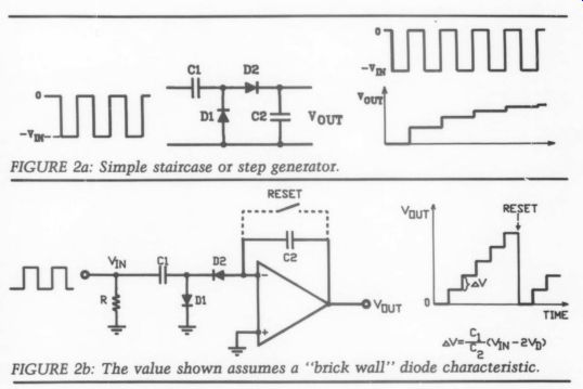
FIGURE 2a: Simple staircase or step generator.
FIGURE 2b: The value shown assumes a “brick wall' diode characteristic.
Vour on the charge and discharge of C1, we can improve the situation by isolating the charge and discharge circuit of C1 from Vr.
This can be done in a number of
---------------
PARTS LIST
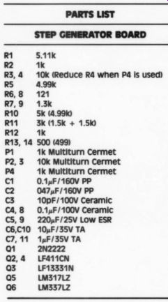
STEP GENERATOR BOARD
5.11k 1k 10k (Reduce R4 when P4 is used) 4.99% 1.3k 5k (4.990 3k (1.5k + 1.50 1k 500 (499) 1k Muititurn Cermet 10k Muititurn Cermet 1k Muititurn Cermet
0.1 uF/160V PP
047uF/160V PP 10pF/100V Ceramic
0.14F/100V Ceramic 2204F/25V
Low ESR 10uF/35V TA 1uF/35V TA 2N2222 LF411CN LF13331N LM3171.2 LM3371.2
------------------------
ways. The one I am using is based on replacing C2 with a Miller integrator (Figs. 2b°>'°).
As I was interested in generating a positive-going step, and the Miller integrator reverses the polarity, I reversed the diodes and fed the step generator from a positive pulse. Each positive going pulse is charging C1 through D1.
As the pulse returns to zero, C1 discharges through D2, drawing current from the op amp's summing input (minus input). The current is, of course, coming from capacitor C2, (the input of the op amp doesn't draw any current} and the current is causing a voltage to build up at the output. The output volt age is increasing by the charge drawn from C1, and if the time constant Rg x C1 is short compared to the pulse-to pulse spacing, C1 will be charged to Viv, and the output waveform is a stair case with equal steps: Vp, x (C1 / C2).
Brick Walling It The simple diode pump could only pro duce (nearly) equal steps if C2 were very large. In this case, however, the steps would be very small. If you re place C2 with a Miller integrator, the effective value of C2 will be multiplied by the open-loop gain of the op amp:
Ao. x C2, so you are approaching the ideal diode pump. The op amp takes care of the small steps associated with a large C2. Its gain amplifies the small steps.
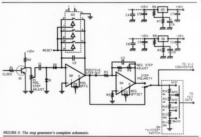
FIGURE 3: The step generator's complete schematic.
Coming back to the staircase generator in Fig. 2b, the actual step size is somewhat smaller than the one mentioned above: there is a voltage drop across the diodes, which we ignored up until now. The value shown in Fig. 2b assumes a “brick wall' diode characteristic, but is good enough for an approximation. In any case, the step's required size is set by adjusting the amplitude of the input pulse, as you will see.
Since you wish to use this staircase or step generator for a curve tracer, varying the number of steps is important. Naturally, the step generator would only run once from zero and up, until the op amp saturates, and then it would stay there forever, unless in some way you reset it to zero. Now, if ...
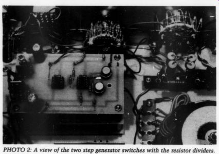
PHOTO 2: A view of the two step generator switches with the resistor dividers.
... you were generating steps with periods of minutes, you could reset the step generator manually. Operating with frequencies of 50Hz to, say, 500Hz naturally prohibits this. Automatic re set can be based either on sensing the amplitude of the staircase, or by counting the number of steps.
Also, the reset can be done a number of ways: using relays, unijunction transistors, or FETs. In my original design, I have been using a unijunction transistor for the reset, which has a disadvantage when used with a Miller integrator: it introduces an offset volt age of approximately 1.2V, which must be compensated to produce the zero base line for the curve tracer. Also, the zero base line changes every time you vary the number of steps. With the many analog CMOS and JFET switches available today, there is no reason to put up with the unijunction transistor's disadvantages.
Figure 3 gives the step generator's complete schematic. Transistor Q1 is used to generate the pulses that drive the charge pump. I have chosen to generate 1V steps, and with C1 = 0.1F and C2 = 0.47F you will need approximately 6V p-p to get it. The step size is adjusted by P1. The reset is done with an analog switch, the LF13331N, containing four switches, three of which I am using. Discharge time is given by R,y x C2, where R, is the
“ON ”-resistance of one FET switch.
With a typical Ry = 200 ohm, the discharge time will be approximately 100uS.
For low-frequency operation, such as 50Hz or 60Hz, one of the switches is enough. (The period of a 50Hz square wave is 20mS, much longer than the discharge time of 100uS.) If you contemplate running the step generator at much higher frequencies, it might be necessary to use the three switches to discharge C2 fast enough. I used three switches because I wanted to try to run the curve tracer at about 500Hz. For reasons described later, I gave up this idea. You might, of course, find other suitable analog switches for this application.
The only critical requirement is it should be able to switch 10V p-p.
CMOS switches also can be used, as long as you supply the necessary RESET signal to them. There will be more about the RESET signal later. The step generator is working with very little offset. As a matter of fact, I have been using it without offset adjustment for quite some time. To enable you to experiment a bit, I included an offset adjustment. All unity-gain stable FET op-amps will work fine in this socket.
Keep It Simple
Obviously, you can also generate negative-going steps by reversing the polarity of the input pulses and the polarity of the diodes. This requires a complicated switching arrangement. To keep the circuit simple, I chose to generate the negative-going steps with an inverting op amp. Step polarity is then selected by switching between the output of the step generator (+ polarity) and the output of the inverter ( polarity). Again, I included a trimpot to adjust the offset of the inverting amplifier (P3), and to fine-trim the amplitude of the negative going steps (P4). These last two adjustments are not absolutely necessary. Sufficient accuracy can be obtained without them.
The step generator's output is driving two things. The first is a voltage divider, which allows you to set the steps necessary to test FETs. R10-R14 make up a 10 k-ohm divider, giving 1V-0.5V-0.2V-0.1V and 50mV steps. The larger steps are for power MOSFETs and general purpose JFETs. The 50mV steps are necessary for the low-noise Toshiba JFETs you might remember from my RIAA and MC-preamps. If needed, you might select different steps by scaling the voltage divider differently. The second output is driving the voltage-to-current converter, necessary for testing bipolar transistors. Before we embark on this circuit's description, we should look at how the clock and reset signals are generated.
The method described above is only one way to make a staircase or step generator. My friend, Kalman Molnar, suggested trying the circuit based on the LF398 Sample and Hold circuit, whose schematic is in the LF398 datasheet! By replacing the reset-transistor Q1 with an analog switch (LF13333), and using two references at the output, you can generate both positive-going and negative-going steps. The step size is adjusted by a trimpot across the reference diodes. The clock and reset signal requirements are the same as for the step generator described above. This circuit yields extremely precise and stable steps, and can be used in precision instrumentation.
Clock and Reset
As I mentioned before, one way to reset the step generator is to count the number of steps, and, after it reaches the desired number, to send a signal to the analog switch across C2, which then discharges it. Since I decided to generate 1V steps and I am using op amps with + 15V supply voltage, I thought I should be able to generate steps up to + 10V. This means I should be able to count from zero up to 10, continuously.
Molnar easily solved the problem: he suggested using a synchronous decade, or a binary counter from the 74160 family. Figure 4 illustrates the clock and counter circuit.
I am running the curve tracer at 50Hz, so I use a 15V AC signal from the ...
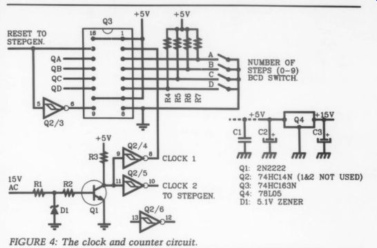
FIGURE 4: The clock and counter circuit.
... power transformer to generate the clock signal. I clamp the positive-going half cycle of the signal to approximately 5V peak with a 5.1V zener diode D1. This is then amplified with Ql. The rise and-fall time of this signal is not fast enough to run the CMOS counter, so I use a Schmitt-trigger (1 of 6 in a 74HC14 package) to speed it up. The clock 1 output is driving the clock in put of the counter, a 74HC163. The counter is counting up from zero until it reaches the number programmed by the data inputs: A, B, C, and D (pin numbers 3, 4, 5, and 6, respectively).
I program with a coding switch, a BCD (binary coded decimal) switch, which allows me to count from 0-9.
The data inputs normally are connected to logic "1" or +5V supply, through resistors R4-R7. When a logical 0" is called for, the switch connects those in puts to ground. In case you have problems getting such a switch, I have given you the logic combination for the 0-9 steps, which can be generated by four simple toggle switches (the A input is the LSB, or least significant bit, D is the MSB, or the most significant bit):
PARTS LIST
CLOCK /COUNTER BOARD 2.21k 5.11K 1K 10k
0.1uF/100V Cer.
2204F/25V Low ESR 14F/35V TA.
2N2222 74HC14N 74HC163N 78L05 5.1V zener/0.5W
The counter, after reaching the programmed number of steps, is generating a signal on pin 15, called the 'Ripple Carry,” used as a reset signal for the step generator. Incidentally, this signal also is used to reset the counter itself: it is connected through an inverter to the 'Load' input of the counter (pin 9). The outputs of the counter: QA, QB, QC, QD, are not used in this application.
The clock 2 output is used to drive the clock input of the step generator.
Voltage-To-Current Converter
You can produce steps between 0 and 9 with the clock and counter circuit and the step generator. These are, how ever, voltage steps, and can only drive FETs, which are essentially voltage driven devices. To plot the I--V characteristics of a bipolar transistor, you need to generate current steps for the base: I;. In most of the curve tracer designs mentioned in the references, this was accomplished by using a series resistor at the output of the voltage-step generator.
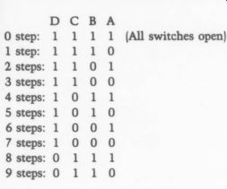
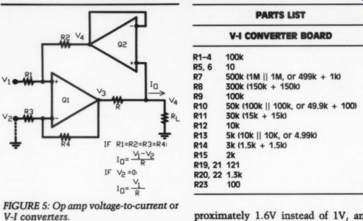
FIGURE 5: Op amp voltage-to-current or V-I converters.
Imagine you have a voltage step of 1V/step, and you want to generate I steps of 1uA. All you need do is connect a resistor of 1M ohm in series with the base of the driven transistor, and each 1V step will produce a 1V / 1 M-ohm =1uA base current step. This is simple enough. You must, however, remember you need about 0.6V to turn on the base-emitter diode, so the first current step would actually be: (1V-0.6V) / 1 M-ohm = 0.4uA instead of the 1uA you wanted.
The next step would, of course, be properly spaced relative to the first one, because (2V-0.6V) / 1 M-ohm = 1.4uA, which is exactly 1A more than the first, and so forth. At first glance, only the first step is “wrong.” The first problem using a series resistor to convert a voltage step to a current step is an off set problem with the first step. An off set problem is easy to solve: ‘compensate' for it. Most of the designers mentioned in the references offset the volt age step to start the first one from approximately 1.6V instead of 1V, and then all of the steps should be correct.
This offset was adjustable to make sure the base line was, indeed, at zero for the different transistors.
------------------------
PARTS LIST (see above)
------------------------
The second problem stems from the fact the base-emitter diode doesn't have "brick wall" characteristics. In other words, the base-emitter voltage is not the same at all collector currents; it is increasing exponentially (refer to Fig. 13a in Part III of my series, TAA 3/90) so even if the first step is adjusted correctly, the second one will be slightly off, the next one a bit more, and so on.
This makes large differences, especially with power transistors, when you are entering the saturation region, and the base-emitter voltage starts to significantly increase. You might ask: what is the solution? Fortunately, we can easily build a true voltage-to-current converter using a couple of op amps.
I have found the two op amp voltage to-current or V-I converters (Fig. 5) in one of the op amp data-books.
Although this circuit can handle a differential input, I am using it with a single, non-inverting input, that is, V2 = 0 or ground.
The actual input voltage on the positive input of the op amp is the sum of V1 and the output voltage V4 (which also appears on the output of follower Q2), divided down with R1 and R2:
R2 R1 Vier tre
Note the contribution from V4 is in phase with the input signal, that is, you have a positive feedback. This is what makes the circuit a nearly perfect V-I converter: the positive feedback in creases the output impedance to a very high value, the characteristic of a true constant current source.
The input signal is amplified by the gain of Q1, which is equal: (R3 + R4) / R3. If you make all resistors equal (R1 = R2 = R3 = R4), the output current ...
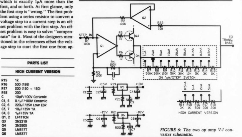
FIGURE 6: The two op amp V-I converter schematic.
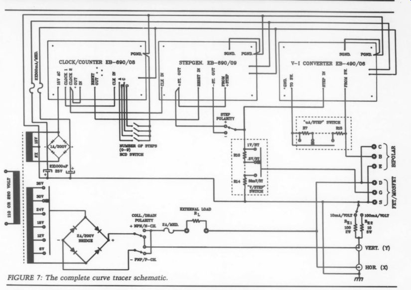
FIGURE 7: The complete curve tracer schematic.
... will be governed by the following simple expression:
Assuming 1V steps are coming from your step generator, you can then ad just the current steps by changing a single resistor: R.
What is the difference between the series resistor and this two-op amp V-I converter? The difference is the V-I converter's compliance, which means it delivers the current set by R, independent of the load resistor, even if the other side of the load is not sitting at zero or ground potential, or if the load resistor changes. In other words, it can automatically compensate for the base emitter voltage of the transistor, and it does that at any collector current. You don't have to adjust the first step any longer, and the steps will be correct, in dependent of the collector current.
Figure 6 shows the two-op amp V-I converter schematic. Notice I have added a complementary two-transistor buffer at the output, because in the 'high current version,’ in Fig. 6, I am drawing approximately 50mA peak cur rent from the V-I converter, when using it with the maximum number of steps.
I have been using old TO-5 transistors from my 'jolly box,’ but feel free to use any transistor delivering 50mA with good hg; linearity. No heatsink is necessary under normal conditions.
The Complete Tracer
Figure 7 is the complete curve tracer schematic. Starting at the schematic's lower left-hand side, notice the power transformer with two secondary windings. (You can use two separate trans formers, probably a good idea if you wish to test power devices.) The upper one is 2 x 15V at approximately 200mA, supplying + 18V to the three boards. The lower one's rating depends on what you intend to do with the curve tracer. If only testing small signal bipolar transistors and small signal FETs, the rating can be the same as the upper one.
The chosen voltages are arbitrary, but when testing new devices always start with a relatively low V; voltage.
This limits the power dissipation in the device, just in case you are running without the external load: R;, and you forgot to set the step generator to its minimum value. The next increments can be equally small, or if you are sure the device can take the higher dissipation, also significantly higher. For convenience, I have selected equal increments of 6V AC, equivalent to approximately 8.5V peak, which gives you a maximum of 50V peak with six taps on the transformer. Naturally, you are free to choose any increment and any number of taps, including much higher volt ages, when checking the transistor's breakdown voltage.
Some designs mentioned in the references used a high power wire-wound potentiometer to set the Vg voltage.
This is possible up to several hundred milliamperes, however, it is not practical for the high current version. A switch and a potentiometer is probably a good idea when you need continuous adjustment. A two-pole switch can connect a 100 / 50W wire-wound potentiometer between two taps of the trans former. This preserves the relatively low internal resistance of the transformer, and gives you the possibility of continuous adjustment. I emphasize again, however, this only works up to a few hundred milliamperes.
Get Thee To A Lab
If you are interested in both small-signal (TO-92, TO-18) and medium power transistors (TO-5, TO-126, T0202, T0220), then the lower part must be rated at approximately 1A, as on the schematic. The bridge (2A / 200V), the fuse, (2A / MED.) and the sensing resistor R; are selected for this kind of testing. If you test power devices in TO-3 plastic and metal packages, then the correct transformer is one rated at 100-200VA. This not only satisfies the current/power requirement, but also ensures that the secondary's series resistance is sufficiently low to avoid load-line limitations. In this case, re duce the sensing resistor to 10. Increase the fuse to about 5A for this kind of testing. Some experimenting will be necessary. Start with a lower value and increase it as required.
The power rating for the sensing resistors are: 2W for the 1000, and about 5W for the 100. I am using an 18W for the 10, and it gets hot when I test TO-3 power devices. The external load R; is needed when looking at the characteristics with a given load resistance. You probably need a selection of these, and plug it into the banana jacks, as necessary. The switch at the secondary of the transformer must be able to handle the maximum collector or drain current during switching and measurements.
As in Fig. 7, I have separate connections (bananas) for the bipolars and the FETs, which simplifies the switching.
As you probably already have guessed, you can only test one device at a time.
The two connectors at the bottom right of Fig. 7 are the BNCs for connecting the curve tracer to your scope. If using an “old" single channel scope turn the time-base switch to the X position.
Both the X and Y channels must be DC-coupled, but you don't nc2d a wide bandwidth on any of the channels.
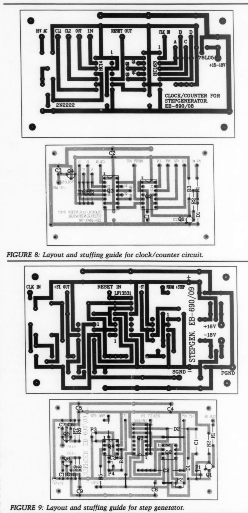
FIGURE 9: Layout and stuffing guide for step generator.
CLOCK/COUNTER FOR STEP GENERATOR.
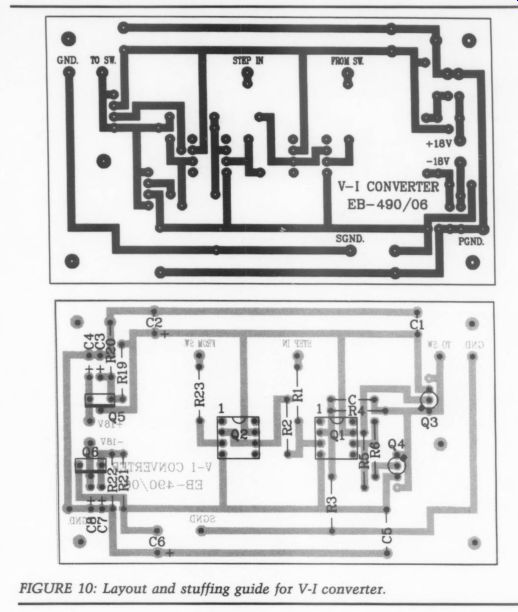
FIGURE 10: Layout and stuffing guide for V-I converter.
With modern, two-channel o-scopes, one channel is normally working as the X and the other as the Y channel, when you turn the time-base switch to the XY position. Follow the instructions in your scope's manual for XY operation and for sensitivity settings.
The upper part of the schematic shows the three boards: the left-hand one is the clock/counter, the middle one is the 1V step generator, and the right one is the voltage-to-current converter, providing current steps for bi polar transistors. Four switches are associated with the three boards. The clock/counter board switch allows selection of the required number of steps. The ‘step polarity' switch is set according to the device tested, and goes hand-in-hand with the collector/drain voltage polarity setting. The following table is an overview of the settings:
COLLECTOR/ DRAIN STEP VOLTAGE: POLARITY:
+ (NPN) +
- (PNP) =
+ (N-CH) -
- (P-CH) -
+ (N-CH) +
- (P-CH) -
NPN (bipolar) PNP (bipolar) N-ch. JFET P-ch. JFET N-ch. MOSFET P-ch. MOSFET The "V/STEP ” switch is for JFETs and MOSFETs.
I test most of Toshiba's low-noise JFETs with the 50mV/STEP setting.
Other general purpose J-FETSs might require the 0.5-1V/STEP setting. The TO-220 and TO-3 Hitachi MOSFETs are tested with 0.2-1V/st settings. You may leave the “V/STEP" switch in any position when no FET is connected to the curve tracer. I suggest you “park” both step switches in the minimum positions between measurements for safety reasons.
Don't Play With Fire
The “uA/STEP" switch allows you to test small signal and medium power transistors with the normal resistor values shown. If you need high current capability, extend the switch with the 'high current version” (Fig. 6). I use a 12-position switch for this version. Incidentally, my highest current step in this version is the same as that offered by general purpose, professional curve tracers.
A word of caution again: this base current is enough to drive most power transistors to approximately 10A collector current! Obviously, the transistors will heat up rapidly when testing them at this high base/collector current, and when you have selected a high value of collector-emitter voltage at the same time. This high-power testing requires utmost care and is not recommended for novice curve tracer users. If you have never before used a curve tracer, I strongly recommend you first build the low-power version, and use it for a while, but design the unit so it can be upgraded later.
I show no details of the power transformer's primary, but use a switch and a slow-blow fuse in series with it, whose size depends on the curve tracer version you are building. Start with a smaller fuse and increase it until you can safely run all your tests. An “ON” indicator, either on the primary or secondary side is prudent. An LED with an appropriate series resistor connected to the +18V is a good solution.
Figures 8, 9, and 10 show the layouts and stuffing guides for the three boards.
You will notice a lot of unused real estate on them. I found it convenient to keep the circuits on separate boards.
If you make your own layout, you may consider putting all circuitry on one board. I have not included a layout for the + 18V supply. You can make a simple one yourself, or you can build it up on a perfboard, possibly locating the fuses there, as well.
(Continued in our next issue.)
REFERENCES
1. Audio Video No. 4, 1989. p. 74.
2. Fasal, J.H., "Build This Transistor Characteristic Plotter,” Radio-Electronics, Sept. 1967.
3. Brassine, P.C., “Automatic Transistor Curve Tracer," Radio-Electronics, Dec. 1969.
4. Mullett, C.E. and C. Caringella, “Build This Transistor Curve Tracer,” Radio-Electronics, June 1972.
5. Metzger, D., 'Transistor and FET Curve Tracer,’ Electronics World, Aug. 1971.
6. Clayton, G.B., "Transistor Curve Tracing," Wireless World, June 1967.
7. Sargent, A.]., 'Electronically Stepped Curve Tracer,' Wireless World, Dec. 1969.
8. Hemingway, T.K., Electronic Designer's Handbook, Business Publications Ltd., 1967, pp. 215-224.
9. Millmann, J. and H. Taub, Pulse, Digital and Switching Waveforms, McGraw-Hill, Inc., 1965, pp. 706-713.
10. Philbrick/Nexus Research: Applications Manual for Operational Amplifiers, 1968, p. 73.
11. Linear Databook, No. 2, National Semiconductor, 1988, pp. 5-13.
12. Burr-Brown Integrated Circuits Data Book, Vol. 33., INA-105 Datasheet, pp. 3-154, Fig. 24.
++++++++++++++++
Also see:
A SIMPLE CURVE TRACER--Part II, By Erno Borbely