LEVEL CONTROL IS one element in music systems that has not yet “gone electronic." We are so familiar with mechanically adjusting gain by rotating or sliding a resistance control element we take it for granted.
Why bother to replace such a simple and reliable element as a sliding control or stepped-resistor attenuator with a 'high-tech' equivalent? Consider a stereo system's requirements. A mono channel needs not be constructed to close tolerances, since a roughly logarithmic (audio) taper of resistance versus position is all that is required.
Matters are more difficult with stereo channels. The best channel balance (tracking) specifications available for dual-channel gain pots seem to be about + 1.5dB. The imbalance can get worse when the signal is turned to low levels.
Another problem with most audio systems volume control is its output resistance variation. As the level changes, the resistance seen by the subsequent electronic stage varies from zero up to a maximum of about one-fourth the control resistance. This variation in resistance causes the audio bandwidth, and the noise floor of the system, to vary with the gain setting. To date, we have had to put up with this effect.
ABOUT THE AUTHOR: William Chater has a BS in electrical engineering, (Cornell '49) and has worked in the nuclear instrumentation field, and more recently with experimental payload design. Mr. Chater builds loudspeaker and hi-fi projects, and is also an amateur violinist.
Just the Benefits
What improvements can we expect from replacing the conventional potentiometer control with an electronic substitute? Here are some of the benefits:
A gain step of, say, 1dB can be made, constant in step size over the whole range.
Two (or more) channels can have the same attenuation on all steps, even to the lowest output level.
Channel balance adjustment can be built into the control by causing one channel to step ahead of the other by one or more steps.
A panel display of each channel's level can be included, showing at a glance the relative signal gain, as well as the system's loudness in advance of a signal.
The electronically controlled attenuator's impedance level can be operated at a mid-impedance level, such as 10k or lower. This impedance reduces the noise floor, and the impedance variation of the circuit output. A conventional volume control can be driven with a unity gain buffer to reduce resistance, but this is seldom done.
An electronic control circuit can include a “default" setting, whereby pressing a panel switch resets the signal channel gain to a pre-set level. This feature is useful in case we desire a standard level, or quick selection of a stand-by gain is needed. The actual default gain can be selected from any level of attenuation available in the design.
Control that Attenuator
How do you make a controllable attenuator? The function can be provided by a basic switchable element, such as an L-pad (Fig. 1). This rudimentary attenuator section produces two gains, approximately unity if the output is sensed by a high-impedance load and the switch is open, or a gain of 1 / (1 + A/B) if the switch is closed. The L section is not designed for matched load use. We could use a more involved ...
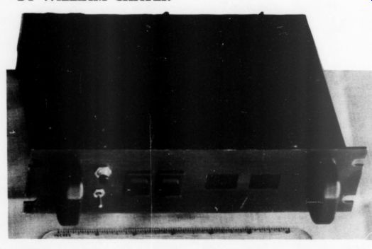
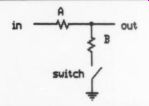
FIGURE 1: A basic switchable element, such as an L-pad.
... matched-load T-section, but it would include more parts, and would com plicate the required switching. For small values of attenuation, the values of resistors A and B in Fig. 1 are com parable: if A = B, the loss becomes 6.02dB. For large values of attenuation, the shunt arm B becomes a small value of resistance: 100 ohm for a 40dB pad having A = 10k.
This scheme naturally produces impedance variations, as seen by the in put signal. A unity-gain amplifier to buffer the input is a solution. Since the system needs buffers for its successful operation, including one such input buffer is not much of a complication.
How can we make a useful attenuator with these L-sections? We can hardly afford 50 or 60 of these, each operated with its own switch, to pro vide a reasonably satisfactory attenuation range. A better way is to use a 1-2-4-8 attenuation step organization
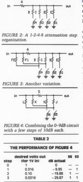
(Fig. 2). Switches S1 through S4 would
----------------
FIGURE 2: A 1-2-4-8 attenuation step organization.
FIGURE 3: Another variation.
FIGURE 4: Combining the 0-9dB circuit with a few steps of 10dB each.
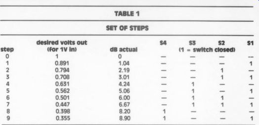
TABLE 2 THE PERFORMANCE OF FIGURE 4 desired volts out (for 1V in)
TABLE 1 SET OF STEPS
... be operated in various combinations. If we make switch S1 cause a 1dB loss, $2 a 2dB loss, S3 a 4dB loss, and S4 an 8dB loss, then we can realize a total of 0 through 15dB in 1dB steps could be realized.
Unfortunately no real set of resistors A through E, as Fig. 2 illustrates, will produce the desired result.
Mathematical solutions for the resistor values show contradictory choices, or negative resistor values. We need another arrangement. The wider our range (0-15dB) the worse this problem gets. If we remove resistor E and reduce the range to 0-7dB with only three switches, the result is less impossible, but still not right.
Figure 3 is another variation. In this case, add new resistor F and relax the range to 0-9dB and we obtain a real set of resistor values. The resulting set of steps is listed in Table 1.
Step Easy
We can now expect to cover the range of attenuation from 0-9dB with four switches. A price has to be paid in steps 4, 7 and 8, which show a 0.2-0.3dB error. Note the switch settings follow the binary pattern from 0-9 in the “binary-coded-decimal” (BCD) code.
Other dB assignments are possible.
Our choice of 1dB per step is arbitrary.
We could use a step size of 1.5dB or some other value, as is often the case in mechanical rotary switch pads. Since we intend to display the step value on a panel readout, the 1dB step is easier to use and is assumed in the design to follow. Again, we could use a straight binary design based on a 0-7dB group, but this would require conversion complications from the binary code to a BCD code for panel readout. (A straight binary readout of bits would work, but would only appeal to the digitally trained user, or to a computer.) To retain the readout feature in decimal characters, I prefer to use the version in Fig. 3 and Table 1, in spite of its step errors.
A 0-9dB attenuator is a good start, but hardly sufficient for an audio sys tem. To extend the design, we need to combine the 0-9dB circuit with a few steps of 10dB each. We see such a design in Fig. 4. This group uses only two switches, and has enough resistors to enable an exact mathematical solution for each resistor value. The performance of Fig. 4 is given in Table 2.
Slight errors result from using standard 1% resistor values.
We see the binary combination of switches S5 and S6 is an extension of the code for the first four switches. To combine the Fig. 3 and Fig. 4 circuits, we need a unity gain buffer to isolate the output impedance of Fig. 3's circuit from the input impedance of Fig. 4's circuit. I suggest a design for the unity gain buffer below.
The combination of Figs. 3 and 4 results in a 0-39dB attenuator in 1dB steps, controlled by six switches. A practical attenuator requires at least 60dB, Fig. 5 be operated in various combinations. If we make switch S1 cause a 1dB loss, $2 a 2dB loss, S3 a 4dB loss, and S4 an 8dB loss, then we can realize a total of 0 through 15dB in 1dB steps could be realized.
Unfortunately no real set of resistors A through E, as Fig. 2 illustrates, will produce the desired result. Mathematical solutions for the resistor values show contradictory choices, or negative resistor values. We need another arrangement. The wider our range (0-15dB) the worse this problem gets. If we remove resistor E and reduce the range to 0-7dB with only three switches, the result is less impossible, but still not right.
Figure 3 is another variation. In this case, add new resistor F and relax the range to 0-9dB and we obtain a real set of resistor values. The resulting set of steps is listed in Table 1.
Step Easy
We can now expect to cover the range of attenuation from 0-9dB with four switches. A price has to be paid in steps 4, 7 and 8, which show a 0.2-0.3dB error. Note the switch settings follow the binary pattern from 0-9 in the “binary-coded-decimal” (BCD) code.
Other dB assignments are possible.
Our choice of 1dB per step is arbitrary.
We could use a step size of 1.5dB or some other value, as is often the case in mechanical rotary switch pads. Since we intend to display the step value on a panel readout, the 1dB step is easier to use and is assumed in the design to follow. Again, we could use a straight binary design based on a 0-7dB group, but this would require conversion complications from the binary code to a BCD code for panel readout. (A straight binary readout of bits would work, but would only appeal to the digitally trained user, or to a computer.) To retain the readout feature in decimal characters, I prefer to use the version in Fig. 3 and Table 1, in spite of its step errors.
A 0-9dB attenuator is a good start, but hardly sufficient for an audio system. To extend the design, we need to combine the 0-9dB circuit with a few steps of 10dB each. We see such a design in Fig. 4. This group uses only two switches, and has enough resistors to enable an exact mathematical solution for each resistor value. The performance of Fig. 4 is given in Table 2.
Slight errors result from using standard 1% resistor values.
We see the binary combination of switches S5 and S6 is an extension of the code for the first four switches. To combine the Fig. 3 and Fig. 4 circuits, we need a unity gain buffer to isolate the output impedance of Fig. 3's circuit from the input impedance of Fig. 4's circuit. I suggest a design for the unity gain buffer below.
The combination of Figs. 3 and 4 results in a 0-39dB attenuator in 1dB steps, controlled by six switches. A practical attenuator requires at least 60dB,...
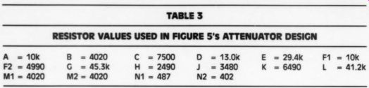
TABLE 3: RESISTOR VALUES USED IN FIGURE 5's ATTENUATOR DESIGN
...which one more buffer and one more attenuation group provides. This final group is a single 40dB pad driven by one switch. Because this attenuator section provides the largest loss in a single step, it is better to use a four resistor 40dB section driven by a double-pole two transistor switch (Fig. 5). This modification produces a 40dB loss without making use of very small resistor values in the shunt arms. The benefit is in removing the need for very small S7 switch
------------------
APPENDIX 1
Expected noise levels in the digital attenuator output.
The attenuator is a mix of active and passive parts, so you might wonder how to estimate the system's expected noise output. With active circuitry, noise performance might well be worse than in a simple passive attenuator. The digital attenuator’s output noise level is determined partly by the three unity gain buffers, and partly by the resistors, which make the various dB steps.
The thermal noise of these resistors is that of Fig. 5's three resistance groups connected in series. This is worst case at the 0-dB setting, because the three groups add their noise powers without attenuation. With the A group = 3730 ohm, the G group = 6418 ohm, and the M group = 80400, the expected thermal noise floor from these resistors at room temperature is 2.454V RMS in a bandwidth of 20kHz. This is 112.2dB below 1V RMS.
Expect further noise from the three unity gain buffers of about 1xV RMS each in a 20kHz bandwidth. We can vectorially combine all these noise sources, and tabulate the sum for each attenuator setting (Table 4). From this tabulation the noise output is evidently greatest on the 0dB step, and smallest at the largest attenuations.
How do these noise levels compare with a conventional potentiometer? A 100k pot alone at room tempera ture would have a thermal noise across it of - 105dBV (about 5.75uV).
In a circuit, however, it would have its greatest noise output when set to a 6dB loss, where equal resistance is presented above and below the center tap. The circuit would see these equal resistances in parallel, or half the above noise, about 2.9uV (-111dB).
The pot circuit's signal-to-noise ratio at the 6dB setting would be 105dB. We find the same performance with the electronic attenuator. The two methods follow closely over the dB range from 1dB down to about 20dB of attenuation. Below this, the potentiometer noise is less, because of the buffer amplifier's noise floor in the electronic version. The new circuit will operate as well as the part it replaces, from a noise point of view.
OUTPUT NOISE IN dB BELOW 1V
------------------
... resistance. (Dependence of the 40dB attenuator on switch S7 resistance is about 0.22dB/Q of S7 resistance change for the one-transistor design. Changing to the two-transistor design (Fig. 5) reduces this dependence to about 0.033dB/9.) Our circuit now looks like the design in Fig. 5, with three unity gain buffers.
The circuit covers the range from 0 79dB in 1dB steps with seven switches.
This control should give sufficient range for an audio system. We could add a fourth unity gain buffer at the output, but since the circuit to follow will probably have relatively high impedance. I did not include it. If the output load is 100k, then we can design the final attenuator to give a 40dB loss when we close switch seven, compared to the loss with switch seven open. I have included this adjustment in the circuit in Fig. 8. The 1dB fixed loss can be made up by raising the third buffer's gain to 1.12, or the 1dB loss can be accepted because of the 100k load, resulting instead in a 1-80dB design. Resistor values used in the attenuator sections are given in Table 3.
Our design uses seven switches. This requires a seven-bit BCD switch controller, which operates the attenuator over its code range of 80 steps, and controllable from the panel. The seven switches must be capable of good linear bipolar action. Let's consider this “analog” switch's details.
The Switch
We see from Fig. 5 the analog switch must be able to provide low resistance, compared to the lowest value of the shunt arm of the attenuator stages.
Resistors N1 and N2 are the design's lowest values, and call for switch resistance as low as 10 ohm. If the actual switch resistance is known, it should be subtracted from the shunt arm resistor to maintain accuracy. (The values in Table 3 already include this correction.) Various switch designs are possible.
For example, a simple npn transistor can short the bottom of the shunt elements to ground, when switch conduction is called for. A bipolar device has the drawback of a feedthrough voltage off set. It also exhibits a nonlinear resistance, different for positive than for negative collector currents. This resistance is also likely to be larger than we would like for negligible effect on attenuator distortion. Also, a bipolar is unable to stand off more than about 0.5V peak ...
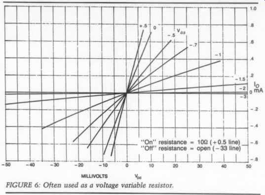
FIGURE 6: Often used as a voltage variable resistor.
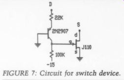
Fig 7 .
... before the reverse collector-base diode comes into conduction. Some of these faults can be avoided, but some could cause audio signal distortion.
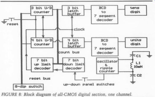
FIGURE 8: Block diagram of all-CMOS digital section, one channel.
A junction FET makes a better switch. Often used as a voltage-variable resistor (Fig. 6), the JFET has the advantage of showing no feedthrough offset, the only error current being one through the reverse drain-to-gate capacitance (Cgrss), which is usually very small.
Resistance the JFET provides can be modulated from open circuit to some small resistance value, and is quite linear and straight-line through the origin. This performance produces a low-distortion output signal, even if the Ips (on) is a noticeable fraction of the attenuator shunt resistors. The JFET I chose is the J110, an n-channel JFET having a cut-off gate voltage rating from 0.5-4.0V (Vg off) and an 15 (on) of 101 (typical). The J110 Cg rating is 15pF.
A Better Mousetrap
Other switch design choices are possible, as in Fernando Viesca's article
“Digital Gain Controls,” in TAA 3/89.
Other switch designs might work here:
the diode bridge, the MOSFET transistor, and, of course, the relay. A diode bridge is often used in radio-frequency designs, where it needs a transformer easily fashioned for high frequencies.
The transformer's presence, and low level audio nonlinearities, make the scheme a dubious one for audio work.
The MOSFET offers a good linear, low ON-resistance, but has two features we don't want: a relatively large capacitance, and a reverse substrate diode. Ad ding a series MOSFET of the opposite polarity is a way of coping with the reverse diode, but the resulting switch, although very good, is a little too complex to be replicated seven times. A reed relay is an ideal switch for our purpose, but creates an unwelcome power demand.
If this were the only cost, I would accept the power loss and use the reed in each of the seven switch points, but its slow operate time, and even slower release time are undesirable. The design would require some rather carefully adjusted and complicated delay circuits to prevent the step-by-step dB settings from momentarily faulting to an un wanted dB value, not necessarily intermediate to the step points; not a trivial problem. Consider the case when stepping from - 39dB to -40dB. If the 40dB relay closes before the 39dB can drop out (that is made up of the 20, the 10, the 8, and the 1dB switches when closed), there would be a few milli seconds of -79dB gain.
This flaw would sound like a signal drop-out, and would require a delay in the application of drive current to the 40dB switch, so as to fill in the gap.
Switching from -40 to - 39dB would again switch the attenuation via the -79dB step. Relays almost always display faster pick-up time than drop out time, and reeds are no exception.
Since their actual delays are not accurately known, driver delay adjustment would be complicated. Finally, if the delay were over-compensated, a step from - 39 to -40dB via zero dB would result, which would be unpleasant indeed.
I have chosen to use the JFET as our switch device whose circuit is in Fig. 7.
Seven copies occupy relatively little card space. A logic input of zero volts or + 5V is applied at the digit terminal D, which:
1. $1 and S2 are either DPDT center-off panel toggles (as shown) or can be dual DPDT normally-open push-button switches (4 buttons for a stereo channel) (see Fig. 16)
2. A different tap at the clock take-off (pins shown on right edge of 4060 oscillator chip) can be selected to alter the step rate clock. If desired, the additional rate Fig. 17. selector switch S4 can be included (see dotted box).
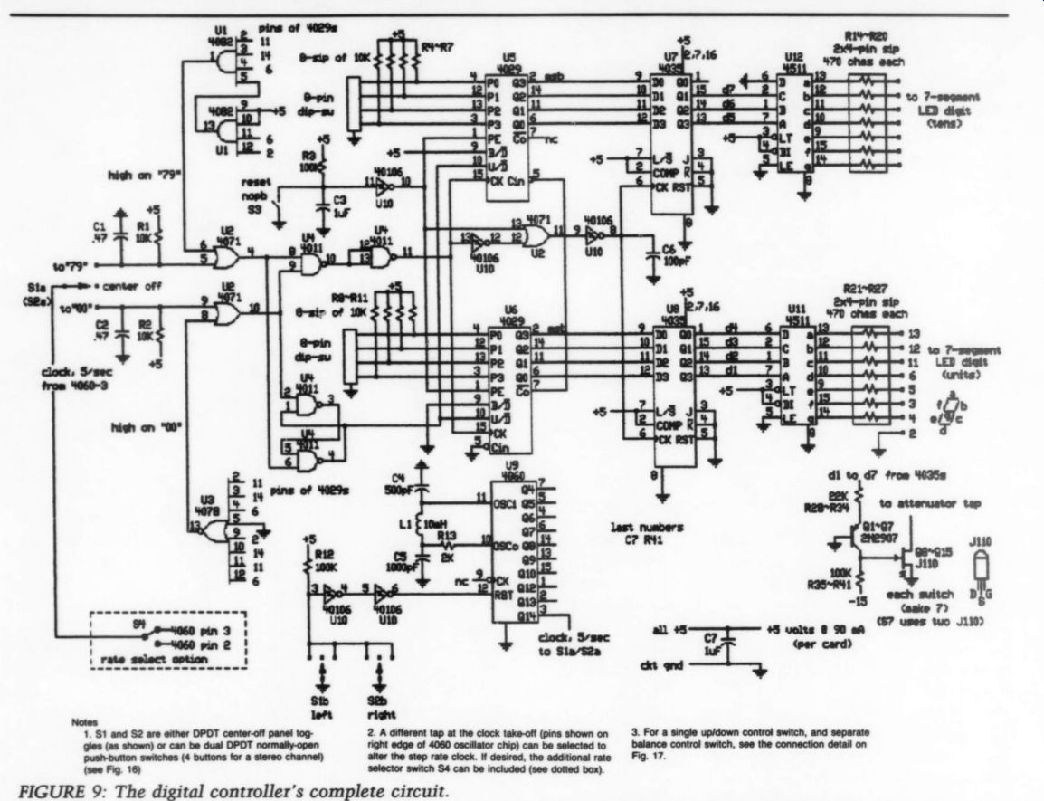
FIGURE 9: The digital controller's complete circuit.
3. For a single up/down control switch, and separate balance control switch, see the connection detail on drives the JFET gate with two levels, +0.6V or - 15V. Since the JFET is sym metrical, its source and drain can reverse roles when the audio signal voltage at the switch point S crosses zero. A negative audio voltage at S of up to - 10V can be applied to a JFET having a Vg (off) rating of 5V or less, before undesired reverse switch conduction occurs. Our J110 meets this requirement. A positive audio voltage at S of up to the V_DS transistor rating is allow ed (25V for the J110). When ON, the device shows the small linear resistance value 1, (on) to either audio polarity (Fig. 6). The J110 is appropriate for use in all seven switch positions.
The Digital Driver Circuit
Now let's turn to the digital control requirement: how do we drive the seven digit (D) switch points? We can take ad vantage of the plenitude of low cost binary circuits, having almost any binary function desired. One channel's
[...]
A seven-bit binary up-down counter Storage latches Two BCD-to-seven-segment decoders Logic gates for up and down limits An LC oscillator A default code selector switch
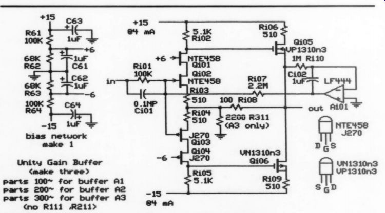
FIGURE 10: Roll your own when it comes to the buffer.
The counter keeps track of the dB set point for each channel's attenuation, and steps up or down in the range 0 to -79dB, at a rate set by the oscillator.
When the step at zero is reached, the gate logic decodes this condition and stops the clock pulse train to prevent the count from rolling over to the - 79 step.
Likewise, a decoder chip at the - 79dB step prevents a roll-over from - 79dB to the zero dB step. The dB setting is displayed by connecting a pair of seven segment LED chips to the output lines of the BCD decoder. All the logic chips are readily available low-power CMOS, operated on a + 5V bus.
Pressing either the up or down panel push button starts the oscillator and steps the up-down counter until the button is released, or the range ends. I chose the oscillator rate for stepping at about 5dB per second, fast enough to change gain, but not so fast to prevent selection of a single dB step. Change L1 or its associated capacitors to alter the rate. You can also change step rate by reconnecting the clock's binary take-off point. Since the oscillator chip is a ripple binary counter, all factors of two (except Q11 of the oscillator chip) are available.
Wiring more sets of switches to the panel allows you to tailor the system for multiple step rates. The oscillator could be a crosstalk source from binary noise in the system. To prevent this, I designed the oscillator to operate above the audio band, at a base rate of approximately 81kHz. When you release the panel switch, the oscillator reset line is activated, stopping the oscillator. Only when a call for a new attenuator setting (of either channel) is made does the 81kHz oscillator start.
The audio signal thus is free of any binary system noise.
Click-free Stepping
The digital buffers hold each binary count value, and only re-load at the '“half-clock” time to prevent a false counter code from momentarily sending the switches an unwanted attenuator setting. False timing might occur if a clock were to set the two counter chips at slightly different times, per haps making a click in the output. The digital buffers assure that only legitimate codes are sent, and that all the dB switches operate at the same instant, within a fraction of a microsecond, pro viding click-free stepping. The preload inputs of the up-down counters force the counters' binary value to copy the default code value previously set into the eight-point dip-switch. At power on, the default value is forced into the counter to preclude having to manually reset the system. The whole digital sys tem operates from + 5V at a few milli-amperes, mostly for the oscillator.
The binary circuit's low-power operation has one exception. The displays use seven-segment LED chips, which use about 7mA per segment at average brightness. A total + 5V bus demand of up to 180mA is thus possible, which will vary with the numbers displayed.
A + 5V regulator is useful to isolate this varying demand from the rest of the sys tem. If you choose an LCD instead of the LED chips, most of this 1W power demand can be averted.
-----------------
APPENDIX II.
The servo control loops' time response.
It is puzzling at first to see the turn on transience of the unity buffer's servo loop controls as it slowly adjusts to the DC conditions. Why is the apparent time-constant so long? We would expect it to be something such as the 1uF-1 M-ohm (one second) response of the parts in the LF444s.
The following analysis explains how the circuit lengthens this one second time constant. (It is not a problem;
once it settles, the action is over.) Refer to Fig. A. We can write from inspection of the circuit:
1. nV -E -iR =xand2. Vp =x - 1/C (integral of i (n = loss factor of the 100k, 2.2M divider;
n = 0.0435) since the gain G of the op amp is very large, x = -Vp / G will be very small and can be dropped:
3. so from 1)nVp = E + iR 4 and Vp = - 1/C (integral of i) the derivative of 4) gives:
5. dVp/dt = -i/C substituting this into 3):
6. nVp = E - RC (dVp/dt) taking the LaPlace transform of this gives: oV, = -Gy
7. nVp(s)] = E(s)-sRCVp(s) which gives
8. Vols) = Efs)/fn + SRC) =
E(s)/RC{s + n/RC) Here we can introduce a form for the error E.
The step E = E/s is the form to show how the circuit reacts in its effort to null out this step.
9. Vols) = [E/RC|;1/s(s + n/RC}s
10. Vpis) = (E/n) [1/s - 1/{s + n/RCJ]
This transforms back into the time domain as:
11. Volt) = E/n [1 ~ expftn/RC}]
This shows the system will respond with a time constant of RC/n. Since n is the fraction by which the circuit multiplies the servo output before applying it to its own input again, the factor n of about 0.04 changes the time response from a 1 second RC to:
that of a time constant of about 25 seconds. When watching the servos settle, one sees they creep until passing through not one, but three or four of these 25 second time constants.
No wonder it takes a minute.
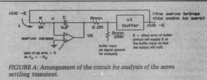
FIGURE A: Arrangement of the circuit for analysis of the servo settling transient.
---------------------
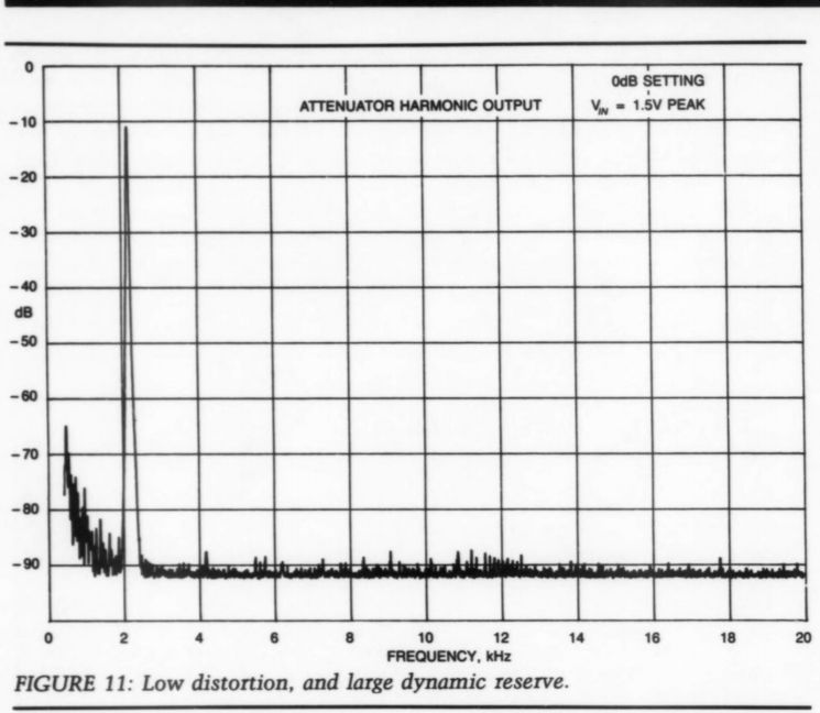
FIGURE 11: Low distortion, and large dynamic reserve.
The Amperex series, available from Digi-Key, is one such LED chip. I have not included it, mainly because its visibility is not as good as that of the LED display. Replacing CD4511 LED with the CD4543B LCD would require re-arrangement of the PC card traces, as these two are not interchangeable.
The LCD also requires a zero DC drive component to keep it from deteriorating. This is usually done by modulating the back-plane of the LCD with a square wave. The possibility of this back-plane drive signal creating audio noise is also reason to prefer the higher power LED.
Figure 9 shows the digital controller's complete circuit, as well as the panel switches and the analog switches needed in the signal path. I suggest a power supply circuit in the design which follows, plus a printed circuit card layout and parts list for all circuitry.
Unity Gain Buffers
The isolation we need at three places in Fig. 5 can be simple op amp buffer.
For example, the BUF-03 of Precision Monolithics Inc. (PMI) can be used, powered from + 15V lines. This chip is specified for linearity to no more than 0.002% errors. Such a buffer should perform well in our circuit. It is a very high speed device, but it operates at a rather large power level, thus requiring a good heatsink. The PMI SSM2131P is also appropriate for low distortion audio. The 2131 operates at a lower power level, and has a very good sym metrical slew-rate of 50V uS. This chip is new on the market, and may be difficult to obtain.
I prefer to roll my own when it comes to the buffer. If you also prefer this approach, I suggest the circuit in Fig. 10, which is a design of quite familiar topology occupying a very small space. It has low distortion, (Fig. 11) and a large dynamic reserve. Since the input signal level will probably always be 1V or less, the circuit has ample headroom. It is controlled by a servo feedback loop to minimize the output offset of each amplifier. The three buffers are served by a single LF444.
Our design has all the sections needed for a complete signal channel, which is comprised of three buffers and the switched attenuator set (Fig. 5), plus a digital control system (Fig. 9). It is practical to assemble one of the attenuators on a single printed circuit card. You can then make multiple channels by duplicating the card. By careful layout, I was able to combine the attenuators and their buffers with the binary controller, without undesirable crosstalk or binary interference. I wanted a small card to permit fitting the attenuator system into existing equipment.
----------
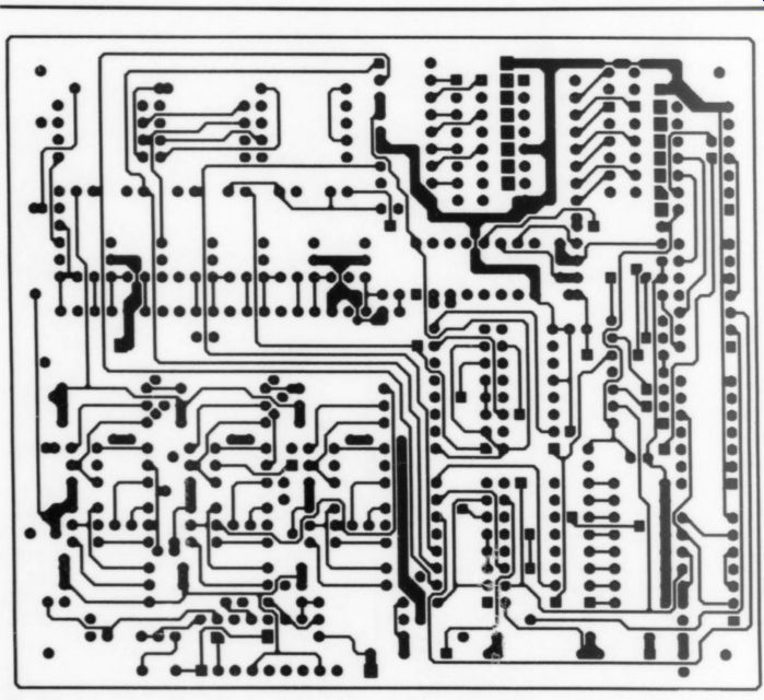
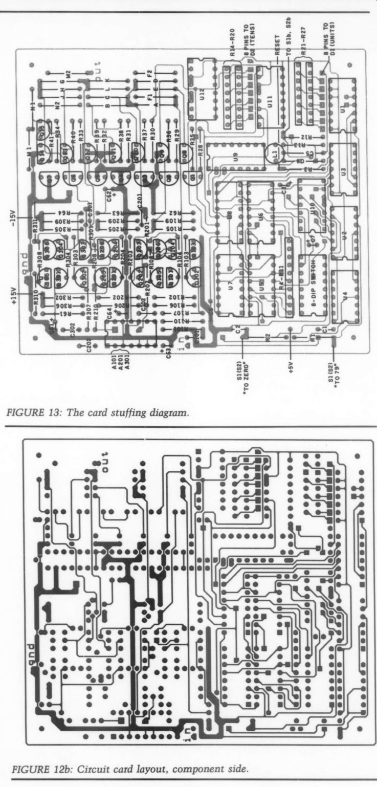
Fig. 12 a
FIGURE 12b: Circuit card layout, component side.
A Printed Circuit Card
Figure 12 shows a suggested printed circuit card layout for one channel of the attenuator circuit. The card stuffing diagram is given in Fig. 13. This 4" by 4.5" densely-packed card includes all the attenuator resistors, unity gain buffers, and digital circuits for one channel. You need two such cards for a standard stereo signal channel. The CD4060 oscillator need be only built on one of the cards, since one oscillator will step both channels. You can also omit parts L1, R13, C4, and 5 on that card.
All other parts are mounted like the card having the U9 oscillator chip. The panel switches are arranged adjacent to each other, so you can easily run both channels in either direction, or step one channel alone. The clock oscillator starts when the switch for either channel is pressed. A separate panel push button resets the two channels to the default setting. The default condition is stored in the eight-pole DIP switch on each printed circuit card.
If you stack the two channel cards, leave enough space between them to set the lower card's DIP-switches. A shield plate of blank printed-circuit card, insulated from the mounting hardware, but grounded to the signal ground minimizes channel crosstalk.
The Power Supply If you choose to add the attenuator sys tem to existing equipment, you'll need +15V at about 12mA and +5V at 90mA at each card. Use a regulator chip, such as the LM7805 with an adequate heatsink for the 5V bus. With the exception of the display power, these requirements are very modest, and can perhaps be taken from the host chassis.
A 5V at 180mA supply can be made up separately for the display circuits. The 5V regulator keeps the LED demands from modulating the logic bus voltage.
A small 6V RMS power transformer secondary voltage would serve to drive such a regulator with about + 8V rectified bus voltage at the regulator input terminal.
If the attenuator chassis already has a toroid power transformer, you might be able to steal a V/A of power directly from it by winding a new secondary of small-gauge insulated wire through the toroid center hole. If you do this, be very careful to avoid shorted turns, as even one small wire shorted through the toroid can damage the transformer.
I suggest you experiment by winding 10 turns first, and measure the open-circuit voltage. From this test you can calculate the volts per turn, and thence the correct number of turns needed to produce about 9V peak (about 6.3V RMS). You can then install a new winding with the correct number of turns, and drive a bridge rectifier and filter capacitor to supply the + 5V regulator.
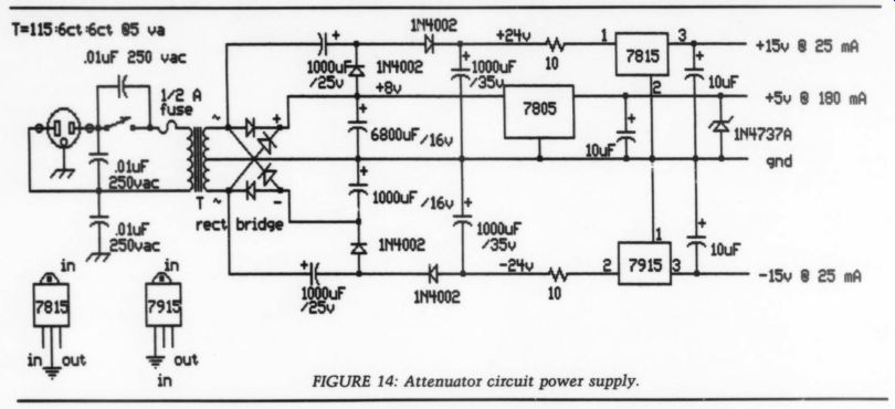
Fig. 14
Before doing this, be sure your toroid transformer can take the additional load.
Avel-Lindberg has suggested a good set of rules to follow:
1. Use correctly rated P.T.F.E.
stranded wire.
2. Space the turns evenly around the core.
3. Avoid a build-up of high spots, if using a disc mount clamp.
4. The transformer's total VA rating must not be increased.
5. Wind the new secondaries over the existing insulation.
You can also build a stand-alone version of the attenuator. In this case, the circuit could be used externally to a preamp chassis, and connected to a tape output, instead of being internally wired into the preamp's circuit. For such a version, I include in Fig. 14 a suggested power supply circuit which would provide all the bus voltages required by a stereo system's two attenuator cards.
Assembly
The PC card (Fig. 12) is double-sided with 591 holes. Circuit continuity assumes a connection is made through the card at many points. A card without plated-through holes can also be used, but you will want to check, as you mount parts, and solder them to the...
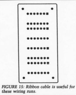
FIGURE 15: Ribbon cable is useful for these wiring runs.
...solder side, to see if a component-side circuit trace is present, which must also be soldered. In some cases a jumper needs to be inserted to join the opposite card traces together through the card (a "Z'-wire”). In some cases, there is no mounted part which will provide the necessary through-card connection.
Install parts in the cards in the following order: all passive parts, resistors, SIP resistors, and capacitors first, then the JFET and bipolar transistors. Mount the 12 CMOS chips and the DIP-switch last, taking care to use a static-free assembly technique, minimizing the possibility of electrostatic damage to the CMOS parts. When assembling the parts next to the DIP-switch, insert the switch first, then the Sip resistor, and then the CD4011 near it, to avoid soldering difficulty.
After assembling all parts on the card, identify and connect to the various power leads, and the points that must be brought out to the panel switches S1, 2, and 3. These connections can be the actual final harness wires, or can be test leads for temporary use. You can make a temporary connection to the panel digit chips, facilitating logic circuitry check-out.
You will want to make a small 1.25" by 2.5 " circuit board to mount the four display chips. Fourteen pin DIP sockets should be mounted on this small board, enabling you to wire the seven-segment display chips to the PC card. Ribbon cable is useful for these wiring runs (Fig. 15). Mount a piece of red plastic as a window over the display with the small board's mounting screws to enhance digit visibility.
Panel Switch Alternatives
Figure 9 shows suggested wiring for a toggle version of switches S1 and 2.
One segment actuates the 81kHz oscillator, while the other sets the desired dB level. You may prefer the center-off DPDT switch as shown, or else four individual momentary DPST push-but ton types. Figure 16 is an example of the connections. The switches in the photos are the Dial-light 572 series.
Reset is a SPST normally-open push button.
The above style of switching gives the operator independent control of each channel's gain. Adjust balance by moving one channel up or down with respect to the other one. Other configurations are possible. Some of you may prefer one control switch to set both channels
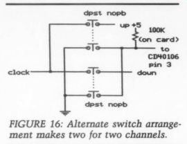
FIGURE 16: Alternate switch arrangement makes two for two channels.
... gains, and another switch for the balance adjustment. The slightly different switch connections (Fig. 17) relieve the user of the need to keep the two channel settings alike as they are adjusted.
Unfortunately, the balance control is now arranged only for reduction of one channel's setting. This scheme leaves one channel unchanged while dropping the other, as is the case with a conventional analog pot balance control. Un fortunately there is no direct way to restore the drop in the lowered channel. Resetting the channels to equa
gains requires lowering the other channel to the same level, and then raising them both. (You could also just push the reset button, which would establish a balance at the default gain setting.
Figure 17's circuit uses two diodes i a logic and gate connection which can easily be mounted on the pane switches. More advanced versions o this diode gating can be invented t customize your design. Another pane switch could be used, for example, t permit raising, as well as lowering the balance control settings.
Testing
First test the digital circuit. A single + 5V power connection is all you need Without the display chips installed, the + 5V bus current should be only a few milliamps, the current required to operate the CD 4060 oscillator. This L-C oscillator's squarewave should be about 81kHz at the 4060's pin 9. The bottom of the frequency divider chain at pin should be about 5Hz. The oscillator should operate only when switch con tact S1b.or S2b is closed, thus applying a ground to pin 3 of the CD40106 chip Grounding pin 3 removes the res term at pin 12 of the 4060, permitting the oscillator to start.
With the LED display chips connected, the + 5V bus current requirement will vary from 25-90uA per channel, depending on the characters displayed. Connecting the oscillator clock source at pin 3 of the 4060 to either the up-line (that is, to 79) at pin 5 of the 4071 or to the down-line (that is to 00) at pin 9 of the 4071 should cause the display to count through its range to the up-limit at a displayed 00, or to the down-limit at a displayed 79. The count should stop itself at these limits.
Do any troubleshooting to obtain this action before proceeding with analog section testing.
You'll use the digital section to help test the remainder of the circuit. When the + 15V power is applied, a bus line current of about 12-15uA each (per channel) should be expected. You can measure this by temporarily inserting some (say, 100) test resistors in the 15V lines to one channel card at a time. If you are using the Fig. 14 power sup plies, check these bus currents by measuring the drop in the 1 0-ohm limit resistors at the input lines to the 15V regulators. Expect variation from the predicted 15mA values, since the operating bias current of the three unity gain buffers is not regulated, but is set ...
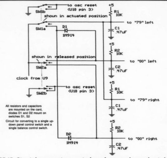
FIGURE 17: Circuit for converting to a single up-down panel control switch, and a single balance control switch.
...in a few millivolts of zero at each buffer output. When these servo adjustment transients have settled (it takes about a minute), the three LF444 op amp outputs should have settled to about zero to + 5VDC. (Refer to the appendix to understand why the bias condition of the servo control loop LF444 of each unity buffer is so slow to settle.) These bias controls will most likely run above zero because the NTEA458's bias voltage requirements are usually smaller than those of the ac companying J270 p-channel units. If the NTE458's match to its J270 mate in each amplifier input pair were closer to equal, the servo would settle at a lower positive voltage.
Socketing one amplifier's NTE458 and J270 input pair, and trying your luck at such a balance is a good way to select minimum-offset pairs of transistors for each amplifier. Unfortunately, the spread I have found is such that the NTE458 is almost always the lower pinch-off voltage unit. You are not likely to find a nicely balanced pair for ever buffer. A closer matching p-channel unit than the J270 would be desirable.
Perhaps you could find a candidate. (I stayed with the J270, in spite of this in equality, because it has a reasonable gain match to the NTE458. Simply discovering a bias match is, of course, not all there is to it). Do a gain test to ensure the attenuator system is working properly. Connect a 1V peak level 1kHz sine wave at the channel input, one card at a time. (If the card power is already turned on when you make this connection, there may be a servo correction transient to accommodate the change in the input resistance you cause by connecting the sine wave generator.)
The test signal should come through the attenuator at unity gain, when the attenuator channel gain is run up to the 00 setting on the LED. Testing for agreement with Table 1's steps should be easy, if you watch the channel's out put with a dB calibrated meter. At each upward (toward 79) dB step, the sine wave amplitude at the output should drop according to Table 1. Lacking a dB meter, simply note the loss from the in put should be a factor of two for each 6dB change. At -6, -12, - 18, -24, and - 30dB the output should be 0.5, 0.25, 1/8, 1/16, and 1/32”, of the input. You could also test this output sequence on a 'scope, or with a linear AC voltmeter.
Circuit Stepping Noise
With each dB level step, the resistance presented to a unity gain buffer changes.
If this resistance change is significant, there will be a slight offset, forcing the LF444 servo to readjust itself. This action is automatic, and causes a slight effect in the audio output. You may notice this in test. For example, when the dB setting steps from 39 to 40, analog switches S1, 4, 5, and 6 (Fig. 5) will open. This causes the signal source resistance at the input to the unity buffer A3 to change from 1406 ohm-6418 ohm. (A much smaller resistance shift also occurs at the input to buffer A2.) The A3 input shift actually adds 5 k-ohm in series with the 100 k-ohm resistor, al ready part of the unity buffer input circuit. This 5% resistance shift causes the small bias correction referred to before. The result is a signal channel transient of about 5% of the servo bias, which makes a small signal disturbance ...
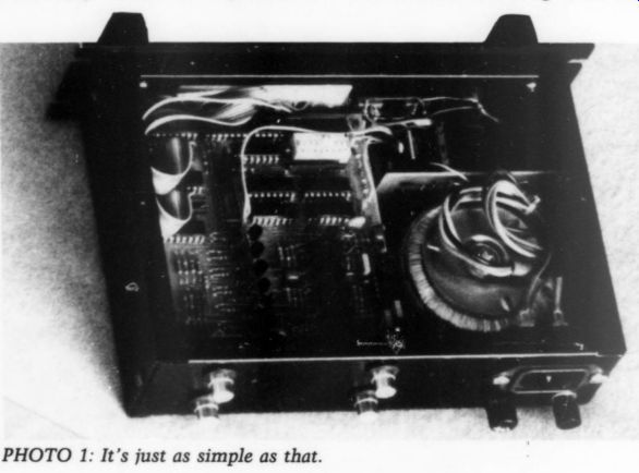
PHOTO 1: It's just as simple as that.
... in the audio. Since this small transient is attenuated in the following section (the A3 attenuator section is set to 40dB loss), the attenuator stepping through its range won't be audible. Signal gain seems to run off smoothly to the inaudibility of the low-end dB settings.
Transient Channel Response
After testing both signal channels, check the transient response if you have a 1kHz square wave test signal and a 'scope. The rise and fall times will be about 1-2uS time constant transients, with the slower response in the upper 40dB (0-39 settings) because of the load capacitance at the output. In the 0-39 settings, the A3 circuitry's output resistance is about 8 k-ohm, giving a 1.6uS response time if loaded with about 200pF.
The noise level should be quite small, and probably hard to observe.
Operation of the complete system is probably the best way to evaluate this noise. Appendix 1 lists the attenuator's theoretical noise level at each step.
Check the system's high-level signal capability, using an input signal large...
---------------
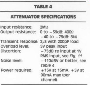
TABLE 4 ATTENUATOR SPECIFICATIONS
Input resistance:
Output resistance:
2 M-ohm
0 to -39dB: 4000
-40 to -79dB: 8k-Ohm 2uS with 200pF load 5V peak input
--75dB re input at 1v RMS input, see Fig. 11
-110dBV or better, see Table 4
+15V at 15mA, +5v at 90mA max (per channel)
Transient response:
Overload level:
Distortion:
Noise level:
Power required:
----------
...enough to see output clipping. Do this at the 0dB setting. The circuit should tolerate an input level of at least 5V peak. One channel's expected 1V RMS distortion is shown in Fig. 11.
Check for crosstalk, too. The shield placed between an installation's two PC cards should reduce any card cross talk. Wiring crosstalk, of course, should be eliminated by care with the signal harness at input and output.
Operation
Before operating the system, I considered possible radio frequency interference (RFI) problems. Some users may find local signal interference, which can introduce undesirable signals into the music. In the attenuator's case, it would be undesirable if such signals entered the circuit's digital controller, and altered the gain setting. I have, therefore, included some precautionary circuitry.
The most likely source of RFI trouble would be from noise entering the switch wiring connected to the up down lines. To prevent this, I designed the R1-C1 and R2-C2 filters with rather low impedances. The 0.47uF capacitors C1 and 2 are mono-lythic ceramics mounted close to the input point, and should suppress any incoming noise pulses before they get to the logic circuitry. The reset line is also filtered in a similar way, with the 1uF tantalum C3. In case of severe interference energy passing through the power supply, I included a zener clamp across the + 5V bus in the power supply circuit.
This should absorb line noises at high frequencies which might get past the power supply's 10uF filter. This clamp
diode also should protect parts from a power surge.
Attenuator operation in listening tests has shown it to be reliable and convenient, and it does not add any "color” to the music. I have tried both the Fig. 9 and Fig. 17 switch connections. It's easy to switch from one circuit to the other, so you might experiment with both. One panel of switches can be used for either circuit hookup.
If the other equipment is powered up when the attenuator power comes on, the attenuator circuit will dwell for a short time (about 100mS) at 0dB gain before the default gain setting takes over. This could give a short full volume start-up.
To avert this, switch to an inactive input for turn-on, or bring up the power to the attenuator along with the power to the other equipment. When attenuator power is shut off, it just fades out, so similar precaution against turn-off noises need not be taken. I have listed the specifications for attenuator operation in Table 5.
++++++++++++++++
Also see: