A SIMPLE CURVE TRACER--Part II, By Erno Borbely, Contributing Editor
AFTER ASSEMBLING and setting up the curve tracer unit (see “The Setup Procedure ” on the facing page), you are ready to make your first test. Before connecting your favorite transistor to the unit, I recommend you go through the following setup. Assuming you will try an NPN transistor first, set the collector/drain voltage polarity switch to + (or NPN/N-CH) and the collector/ drain voltage switch, connected to the transformer's taps, to the first tap. Insert an external 1k-ohm load resistor to limit the current, just in case some thing is wrong. Set R; to 100 ohm, which gives a vertical deflection of 10mA/V.
Set the NO. OF STEPS switch to 2 or 3, STEP POLARITY to +, and the uA/STEP switch to 1uA/STEP. Connect the HORIZONTAL (X) output of the curve tracer to the X-input of your scope and the VERTICAL output to the Y-input (consult your scope manual for this setup).
Adjust the vertical sensitivity (Y) of your scope to 1V/DIV and the horizontal (X) sensitivity to 2V/DIV. If you have a single channel scope, you probably don't have a normal 1-2-5 divider on the X-input, but a 1x and 10x divider. Look this up in your scope manual. If this is the case, you might consider building a 1-2-5 divider to make your tests easier.
Finally, move the dot on your CRT to the bottom left-hand corner of the screen. You are now ready to make your first test.
Connect a small signal NPN transistor to the C-B-E terminals, naturally paying careful attention to the pinout.
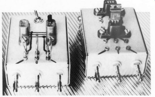
Use short leads to connect the transistor. The leads can be soldered, or you can use just about any kind of spring loaded connectors. If you plan to test many transistors, I recommend you build test-heads with built-in test-sockets (Photo above). Testing speed and long-term reliability will be improved.
Switch on your curve tracer and you should see two or three curves on the scope. Readjust the trace position, placing the base line at the bottom left hand corner of the marker grid on the first marker line.
The vertical deflection, showing the collector current, depends on the transistor's hg, so you probably have to in crease the base-drive to get a useful deflection. Although the basic sensitivity of the curve tracer is defined with your scope set to 1V/DIV vertical deflection, you can increase or decrease this by altering the scope's vertical sensitivity.
For example, if your curve tracer is set to 10mA/DIV (R; = 100 ohm), then you will see 10mA/DIV with the scope set at 1V/DIV vertical sensitivity. How ever, changing the scope to 0.1V/DIV, with the same R; setting will produce 1 mA/DIV.
When testing small signal transistors, you would probably use this setting. For testing at even lower currents, I suggest adding a third position on the R; switch: 1k-ohm would give you a basic 1mA/DIV sensitivity, which can be in creased to 0.1mA/DIV by setting the scope to 0.1V/DIV. Make sure you always stay within the power dissipation limits of the transistor tested. If the external load R; limits your curves too much, you can reduce it. I usually test with R; shorted. This is only advise able if you are an experienced curve tracer user.
To test PNP transistors, reverse the collector voltage and the step polarity.
Since the deflection now will run from left to right and from top to bottom, adjust the dot to the screen's top right corner, and the curves will be displayed upside down.
Connect FETs (J- and MOSFETs) to the D-G-S terminals, which are driven from the V/STEP switch. Testing the Hitachi MOSFETs is similar to the bi polars: N-channels require positive drain voltage and positive steps, the P-channels the opposite. JFETs are different: if you test the Toshiba 2SK147, use positive drain voltage, but negative steps.
The JFET is conducting full drain cur rent: Ic with zero bias, and you need a negative bias to operate at less than Iss. (The top curve is the Ig curve.) Fuzzy Patches? JFETs and MOSFETs have a tendency to oscillate on curve tracers (on all, not just this one), especially with long connecting wires. This shows up as a fuzzy patch on the scope. Connecting a resistor in series with the gate will correct the problem. Connect it as close as possible to the gate pin of the device. I usually use a 100 ohm to 1k resistor, how ever some MOSFETs might require even higher values.
A word of caution with low-noise transistors. If you accidentally reverse bias the base-emitter junction of a transistor, it will degrade its noise performance. Be extra careful when testing these: correct pinout, correct collector voltage, and correct step polarity are essential.
-------------------
The Setup Procedure
As always, I recommend testing the boards before building them into the final chassis. Although you can do the testing using a single channel scope, I suggest you borrow a dual channel from a friend, because this will make life easier for you. You can, for example, display the clock and/or the reset signal on one channel and the voltage steps on the other. All measurements should be done with the scope input switched to DC.
Clock/Counter Board Connect + 15-18V to the board and check that the regulator Q4 is working: the voltage across C2 should be +5V. Apply the 15V AC voltage to the board and check the signal at the collector of Q1. It should be a square wave going from zero to approximately +5V. The rise and fall time will be very slow. Now check the CLOCK 1 and CLOCK 2 outputs.
They are inverted compared to the collector of Q1, and at the same time the rise and fall time is very much faster than the signal at the collector.
If everything is OK, you can connect the CLOCK 1 output to the CLOCK IN pin on the same board, and check the counter. If you are using a coding switch and it is connected to the four inputs: A, B, C, D, then connect the second channel of your scope to the RESET output and check that the RESET pulse is properly delayed relative to the clock signal. If you are using four toggle switches to simulate the BCD code given in the article, then try to set up several of the codes, and check the reset pulse on the scope. You don't have to spend more time on this at this stage. The final test will be done together with the step generator.
Step Generator Board
Connect = 18V to the board and check that the two regulators are working properly. The voltage across C5 should be + 15V and the voltage across C9 is --15V. Connect the CLOCK 2 output from the clock/ counter board to the CLK IN pin on the step generator board and the RESET OUT to the RESET input.
Select 1V/DIV sensitivity on your scope and align the trace on one of the lower marker lines with shorted input. Connect your scope to the + STEP OUT pin and monitor the positive going steps. Set the NO. OF STEPS switch to three or four and check that you really have the same number of steps.
Next, adjust the offset trimpot P2 until the zero step line is again on the marker line. If the step size is not 1V/step, then adjust P1 until the steps are lined up on the 1V marker lines on the scope. Make sure the zero-step line is still lined up on the marker line. Go through all steps from zero to nine. They should all be 1V apart. While changing the number of steps, the position of the zero-step line should not move at all.
Connect the + STEP OUT to the in put of the unity gain inverter (FROM + STEP) and move your scope probe to the - STEP OUT. The zero-step line should still be on the same marker as before, however, the steps are now going in the negative direction, so you should move the trace of your scope to the top of the screen to see all the steps. Again the step size should be 1V. If you find the negative input has an offset, or the step sizes are not exactly 1V, then you should install P3 for offset control and P4 to adjust the negative step size. Using FET-input op amps, this normally will not be necessary. The step generator testing is now complete.
Voltage-to-Current Converter
Connect +18V to the board and check whether the regulators are working. Connect the + STEP OUT from the step generator to the STEP IN pin on the V-I converter. Then connect a 1k/1% resistor between the pins marked TO SWITCH and FROM SWITCH. With this resistor you should get 1mA/step from the V-I converter. However, you have no load connected to the output, so you cannot check whether it is working.
Connect, therefore, another 1k/1% resistor from the FROM SWITCH pin to ground and connect the scope probe across this resistor. You should now see exactly the same steps across the resistor as those at the input of the V-I converter. (What you have done is convert the 1V steps to 1mA steps and then convert the current steps back to 1V steps again.) Make a final check on the V-I converter when you have wired it into the unit and the uA/STEP switch is connected.
Complete Unit
After wiring all three boards into the chassis, again check all voltages.
Make a quick check of the step generator and the V-I converter, as de scribed before. Connect your scope to the G(ate) connector on the front panel and make sure all steps are correct. Test two or three values of the current steps by connecting a resistor between Base) and the E(mitter) terminal and confirming the reconverted voltage steps across the resistor (100k resistor will give you 10 uA/step, 10k is 100uA/step, and so forth).
Connect your scope to the left hand side of the External Load terminal and verify the polarity and the peak value of the voltage you will use for Vi; (X-deflection). You will see a full-wave rectified signal, where the peak value will be the AC voltage multiplied by 1.41. At this point you are finally ready to make your first measurement.
-------------------
------------
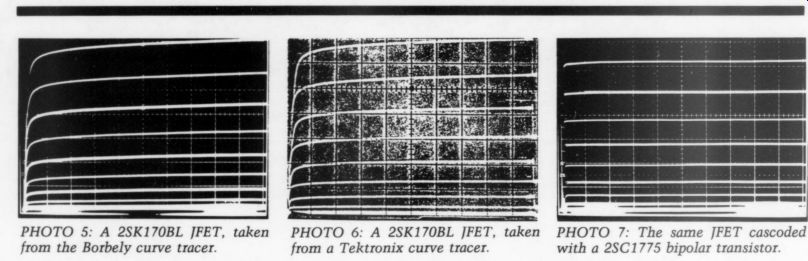
PHOTO 5: A 2SK170BL JFET, taken from the Borbely curve tracer. PHOTO 6: Taken from a Tektronix curve tracer. PHOTO 7: The same JFET cascoded with a 28C1775 bipolar transistor.
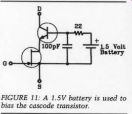
FIGURE 11: A 1.5V battery is used to bias the cascode transistor.
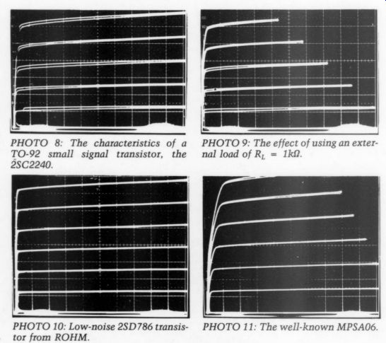
PHOTO 8: The characteristics of a TO-92 small signal transistor, the 28C2240.
PHOTO 10: Low-noise 2SD786 transistor from ROHM.
PHOTO 11: The well-known MPSAQ6.
-------------------------
Now let's look at some real measurements. The pictures have been taken off a Tektronix 465B scope's screen by my friend Josef Peintner, a professional photographer. After comparing all the pictures with photographs taken from a Tektronix curve tracer, I couldn't see any significant difference, except when the trace hasn't been adjusted correctly or when the device has been heated up more on one curve tracer than the other.
Photos 5 and 6 show a 2SK170BL JFET, taken from my curve tracer and from a Tektronix, respectively. Note that the Tektronix has ten vertical divisions, the scope only eight. Except for a slight difference in trace alignment, the two pictures are identical. As I mentioned before, JFETSs are different from bipolars: they conduct maximum cur rent with zero bias, that is, the top trace is showing Is with Vg = 0V. The steps are -50mV each, and it takes just a bit more than -400mV gate-source bias to turn off the FET.
You notice the drain current doesn't decrease in equal steps with equal increments of bias. Also, the characteristics are not flat on the top, indicating a limited output resistance. This also contributes to the static nonlinearity. I have calculated 60k at I, = 5mA.
(Try to read the change on the second trace from the top: the drain current is changing approximately 0.2mA over a drain-source voltage change of 12V, giving 12V/0.2mA = 60k-ohm.) As I pointed out in Part IIT in my series on nonlinear distortions (TAA 3/90), you can increase the output resistance and improve the static nonlinearity by using a cascode circuit. Photo 7 shows the same JFET: 2SK170BL, cascoded with a 28C1775 bipolar transistor. For convenience, I am using a 1.5V battery to bias the cascode transistor (Fig. 11).
The characteristics now are flat, indicating a very high output resistance.
The spacing between the traces is still the same, indicating the typical square low characteristic of the JFET.!3 Photo 8 shows the characteristics of a popular t2SC2240 (PNP complement: 2SA970). It has a 120V breakdown volt age, and can be used as an input transistor in power amplifiers. It has very good hg; linearity, but its output resistance can be improved by cascoding it with another transistor, making it an almost ideal input device. Photo 9 shows the effect of using an external load of R; = 1k-ohm.
Photo 10 shows the low-noise 2SD786 (complement: 2SB737) transistor from ROHM, indicating a very good hg; linearity even at higher collector currents. Due to its relatively low collector-emitter breakdown voltage of 40V, its use is limited to low-voltage, low-noise applications. Photo 11 shows the well-known MPSAQ6 (complement: MPSAS56). This is actually a high cur rent device; however, its normal TO-92 package has a limited power dissipation.
It is also available in a TO-92 power package, with increased power handling capability. Linearity is very good, and cascoded with a suitable device, it serves very well in a medium current driver stage.
Photos 12a and b and 13a and b show a complementary pair of medium power TO-220 devices: the 2SC2592 and 2SA1112. They are rated at 180V breakdown, and a maximum collector current of 1A. Jim Bongiorno used a lower volt age version of these in his Ampzilla III amplifier. [14] Both the NPN and the PNP are very linear and have low saturation voltage up to approximately 100mA. At higher currents, linearity is severely limited (Photos 12b and 13b). You can use these cascoded with themselves or as cascode transistors for MOSFETs, pro viding very good, high current drivers.
---- ----
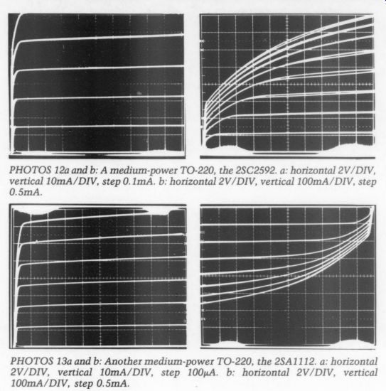
PHOTOS 12a and b: A medium-power TO-220, the 2SC2592. a: horizontal 2V/DIv vertical 10mA/DIV, step 0.1mA. b: horizontal 2V/DIV, vertical 100mA/DIV, step.
PHOTOS 13a and b: Another medium-power TO-220, the 2SA1112. a: horizontal 2V/DIV, vertical 10mA/DIV, step 100pA. b: horizontal 2V/DIV, vertical 100mA/DIV, step 0.5mA.
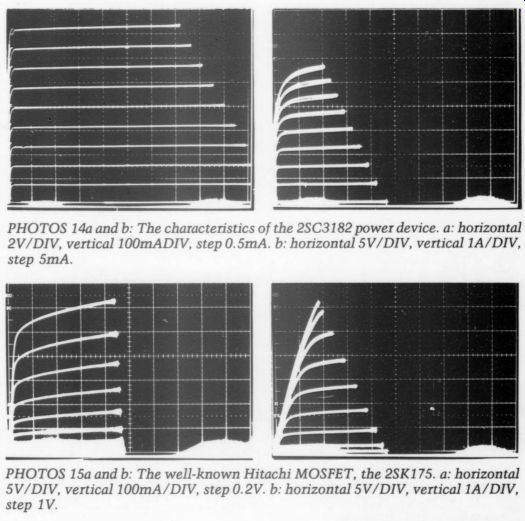
PHOTOS 14a and b: The characteristics of the 28C3182 power device. a: horizontal 2V/DIV, vertical 100mA DIV, step 0.5mA. b: horizontal 5V/DIV, vertical 1A/DIV,
PHOTOS 15a and b: The well-known Hitachi MOSFET, the 2SK175. a: horizontal 5V/DIV, vertical 100mA/DIV, step 0.2V. b: horizontal 5V/DIV, vertical 1A/DIV, step 1V.
----------------
Photos 14a and b and 15a and b show the characteristics of two power de vices. The first is a bipolar device in a plastic TO-3 package, complementary to 2SA1265, used in some high-end power amplifiers. It is rated at 140vV breakdown, 10A collector current, and power dissipation of 100W. It has very good linearity and low saturation volt age up to several amps. hg starts to fall off above 4-15A, and saturation voltage increases. Photo 14b shows the limitation of my curve tracer: although I am using an R; = 1 ohm for these measurements, the total series resistance is about 2.50. The extra resistance comes from the power transformer.
Finally, Photos 15a and 15b show the well-known Hitachi MOSFET: the 28K175. I am using this with the complementary 25J55 in my DC100A amplifier. You will notice the significantly higher saturation voltage compared to the bipolar transistor.
The transistors I listed were meant to illustrate the capabilities and limitations of the curve tracer, and not necessarily intended to be a selection guide. I will compile a list of transistors later and will share it with you. In the meantime, I hope you will build this simple, very useful curve tracer, and learn more about the transistors
You are using in your amplifiers.
REFERENCES
13. Borbely, E., "A Multi-Tone Intermodulation Meter ” Part 1, p. 8, Fig. 3, TAA 2/89.
14. Bongiorno, |., "AMPZILLA-II, I ” TAA 1/84
ACKNOWLEDGMENTS
Many thanks to my friend Dr. Kalman Molnar for his help in designing the clock/ counter circuit for the step generator. He also reviewed part of this manuscript and sug gested corrections and improvements. His contribution is very much appreciated. Also many thanks to my hi-fi friend, photographer Josef Peintner for his patience during the photographic sessions, and, of course, for his excellent photographs.
++++++++++++++++
Also see: