THE NEW BORBELY PREAMP: THE MODULES
IT IS REWARDING to see the many letters I have received from readers asking me to publish the layouts for the preamp modules described in “Measuring Non linear Distortions, Part 3 ” (TAA 3/90, p. 8). A couple of things happened while I was preparing the documentation for such an endeavor. First, I guess unconsciously, I tried to fit the new modules into my old Borbely Preamp. This was an easy task because the new modules are almost 100% drop-in replacements.
Since I was working on a couple of articles about balanced amplifiers at the time, I also put a lot of thought into how to use these modules in a balanced environment. Some of the application examples and the block schematic of the new Borbely Preamp (Fig. 1) reflect these ideas. 'Balanced Audio Amplifiers' (TAA 1/91, p. 14) describes some of these circuits in detail.
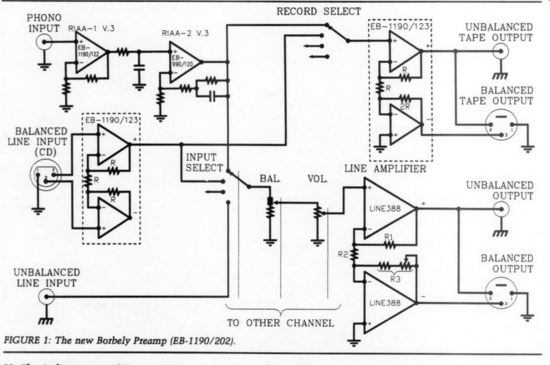
FIGURE 1: The new Borbely Preamp.
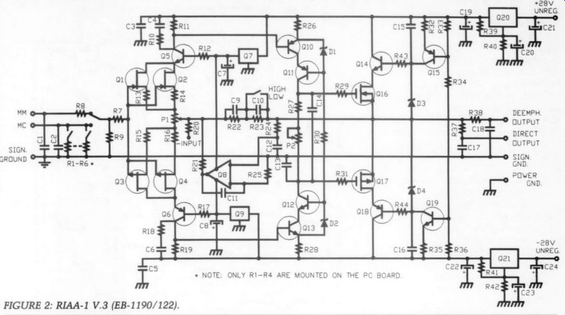
FIGURE 2: RIAA-1 V.3.
Furthermore, the application of these modules is not necessarily limited to preamp use. Take the Class A line amp (Fig. 10), for example: its inherent linearity, low noise, and wide bandwidth make it an almost ideal “general-purpose ” gain-block, and you can use it in professional audio applications like mixer consoles. I show an example of how to use it as a summing amplifier (Fig. 13). Try it in other parts of the audio chain (like upgrading CD players...) and report on your results to TAA.
Each amplifier includes setup procedures, and a pin configuration guide ac companies the devices used in the different modules (Figs. 5 and 9). A separate application guide is provided for the Class A line amp (Fig. 13) and the dual line amp (Fig. 17). Finally, the block schematic, EB-1190/202 (Fig. 1), shows one possible configuration for a semi balanced preamp. It can be converted to fully balanced operation by replacing the volume control with a four-gang potentiometer. Such a fully balanced line amp is shown in the application information given for the dual line amp (Fig. 17).
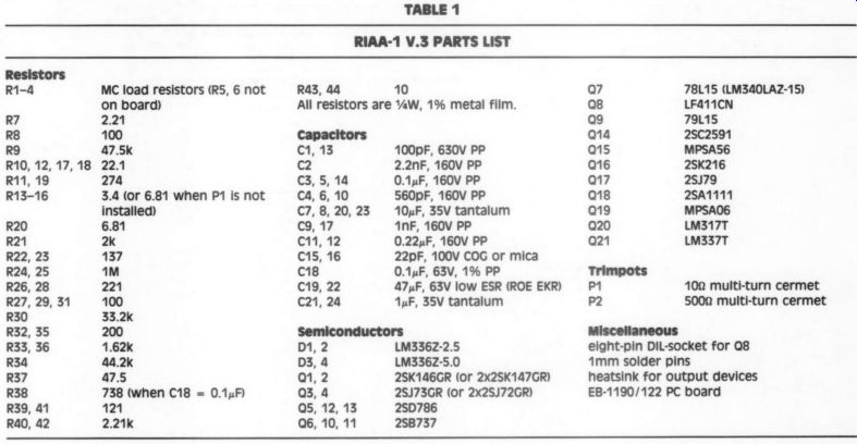
TABLE 1 RIAA-1 V.3, PARTS LIST
----- Miscellaneous eight-pin DiL-socket for Q8 1mm solder pins heatsink for output devices EB-1190/122 PC board ----
Except for a couple of small changes, the schematic of the RIAA-1 V.3 (Fig. 2) is practically the same as Fig. 16 in “Measuring Nonlinear Distortions, Part 3. ” A note on the input devices: although the layout is made for the dual 2SK146/ 2S]73s, you can also use the single 2SK147/28j72s, but make sure you check the pinout for the single ones be fore installing them.
Although I did not try it, you can use only one pair of input devices if you are using moving magnet (MM) pickups.
Let me know if this is of interest and I will send you a proposal. I included a four-pole DIL switch on the layout for MC-loading. You can choose the load resistors according to your pickup. If you prefer to have a switch on the back of your preamp, leave this part of the board unpopulated.
The circuit is designed for 26 and 32 dB gain. The switching shorts out one of the feedback resistors. Although this switching does not disconnect the feed back, it will cause a DC thump because of the sudden change in gain. I suggest you turn your volume control to zero before you attempt to switch gain.
Like the original RIAA-1 V.2, the feed back network has a very low impedance to keep the noise low. It is driven by the output stage so you need a high current amp, especially if you wish it to run in Class A at all signal levels (up to 10V RMS). In the high-gain position, the load is about 2800, and you need approximately 50mA quiescent current in the output stage to drive this in Class A.
Total current consumption of the module in the high-gain position should therefore be adjusted to 75-80mA.
In the low-gain position, the load is approximately one half of the high-gain one, and you need twice the quiescent current-100mA in the output stage.
Total module current should be adjusted to about 130mA. This results in almost 2W dissipation in the cascode output devices, and they have to be heatsinked.
RIAA-1 V.3 EB-1190/122 fod 3
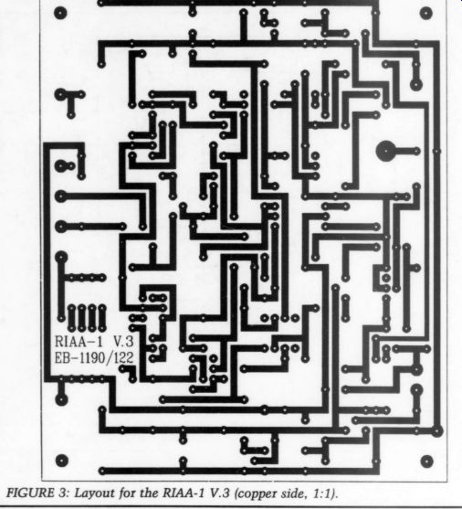
FIGURE 3: Layout for the RIAA-1 V.3 (copper side, 1:1).
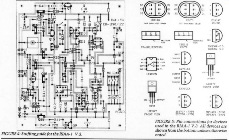
FIGURE 4: Stuffing guide for the RIAA-1 V.3.
FIGURE 5: Pin connections for devices used in the RIAA-1 V.3. All devices are shown from the bottom unless otherwise
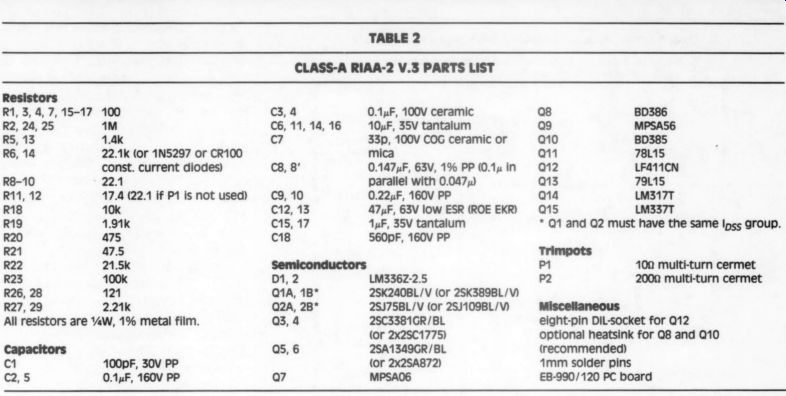
TABLE 2, CLASS-A RIAA-2 V.3, PARTS LIST: Miscellaneous eight-pin DiL-socket for Q12 optional heatsink for Q8 and Q10 (recommended) 1mm solder pins PC board
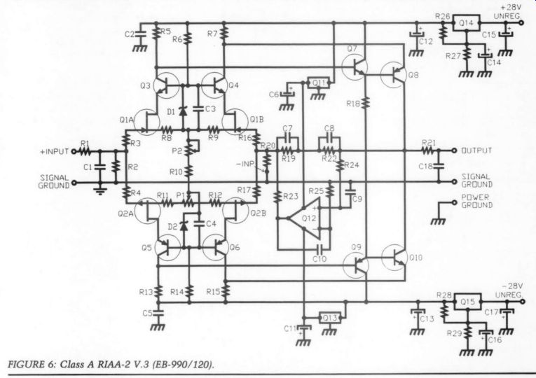
FIGURE 6: Class A RIAA-2 V.3 .
A simple heatsink is indicated on the stuffing guide. Feel free to install any kind of heatsink you think will do the job. Make sure all transistors are insulated from the heatsink (and each other).
RIAA-2 V.3
You will recognize this circuit (Fig. 6) as the Class A line amp, with the feed back network modified to perform the low-frequency compensation, just like in the original RIAA-2. In fact, I have kept the same values here, but refer to the original article if you decide to calculate new values. In choosing the impedance of the feedback network, you have to remember the limited drive capability of the Class A output stage. I have added servo to the circuit; it is needed because the DC gain is very high due to the RIAA compensation.
You can use either the dual 25K240/ 2Sj75 devices in the input stage or, as I show it on the stuffing guide (Fig. 8), the dual monolithic 2SK389/2SJ109.
These devices have almost identical characteristics and can be interchanged without circuit/component changes.
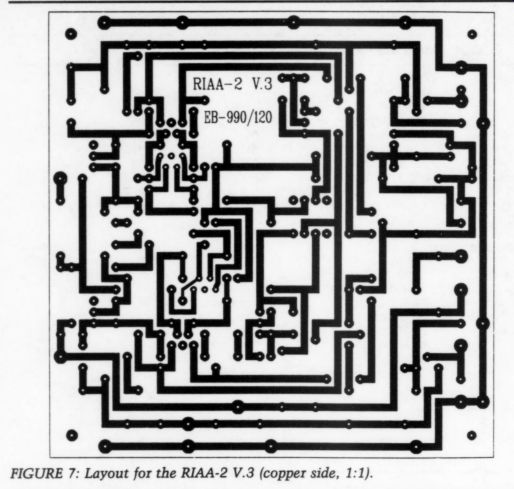
FIGURE 7: Layout for the RIAA-2 V.3 (copper side, 1:1).
Since the 2SK389/2Sj109 have a different packaging compared to the 2SK240/ 28]75, it was quite difficult to accommodate both on the layout. As it turned out, you must bend the pins a bit on both types to make them fit. Examine the pin configuration before you install the devices.
I show a dual monolithic transistor for the cascode input stage. A TAA reader, Mr. Levitzky of Hamden, Connecticut, first brought these 2SA1349/2SC3381 Toshiba devices to my attention. Originally difficult to find, they are now standard input cascode devices in all my new designs. Packaged like the 2SK389/ 2SJ109 monolithic FETs, they require a special layout. The layout (Fig. 7) is made so a single 2SA872/2SC1775 can also be used.
I still use the BD385/386 devices in the TO-202 package for the second stage and they work well. Although I am looking for possible substitutes, I don't have any at the moment. They are running at about 30mA and dissipate approximately 0.7W. Theoretically, you don't need a heatsink for these devices; however, for long-term reliability, I always recommend heatsinking them.
In this case, you can use an aluminum strip, about 0.6 ” wide and bolted to both devices, without insulation.
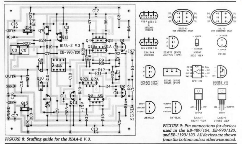
FIGURE 8: Stuffing guide for the RIAA-2 V.3.
FIGURE 9: Pin connections for devices used in the EB-489/104, EB-990/120, and EB-1190/123. All devices are shown from the bottom unless otherwise noted.
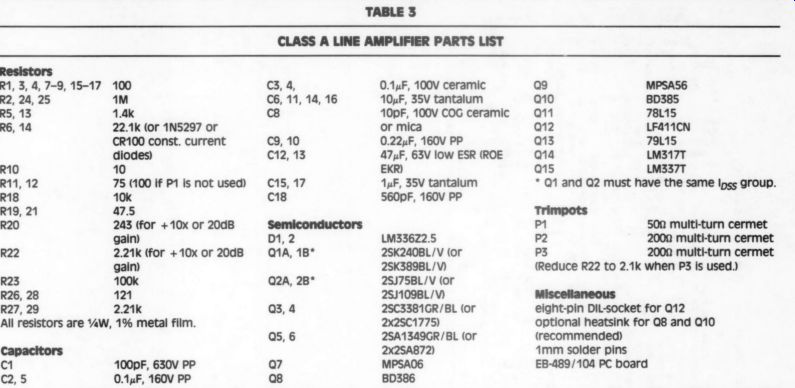
TABLE 3: CLASS A LINE AMPLIFIER--PARTS LIST
--- C3, 4, 0.14F, 100V ceramic Qs MPSAS6, Miscellaneous eight-pin DiL-socket for Q12 optional heatsink for Q8 and Q10 (recommended) 1mm solder pins EB-489/104 PC board, Class A Line Amp (EB-489/104) ---
Again, except for minor modifications, the amplifier (Fig. 10) is the same as the one in 'Measuring Nonlinear Distortions, Part 3'. I added a servo and regulators on the layout so it can be used as a universal gain-block in different applications. Except for the feedback network, the circuit is the same as that of the RIAA-2 V.3.
Dual Class A Line Amp
My article on balanced amplifiers de scribed a number of dual amplifiers with relatively low gain. For low-gain applications, you can operate the Class A line amp without servo, so I left out the servo from the dual layout (Fig. 14).
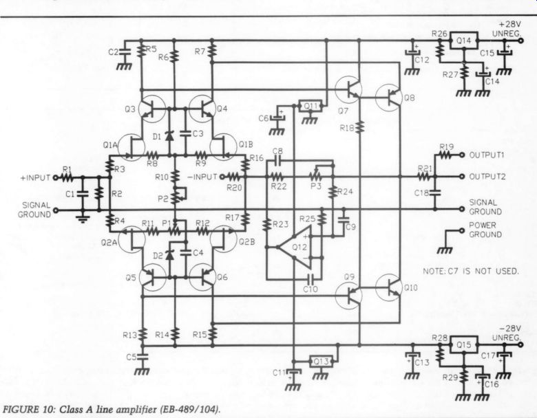
FIGURE 10: Class A line amplifier.
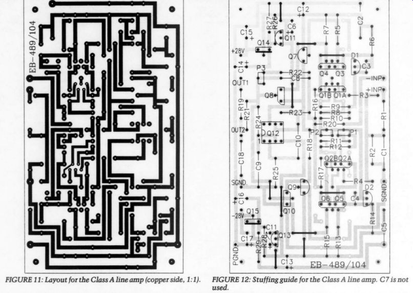
FIGURE 11: Layout for the Class A line amp (copper side, 1:1). FIGURE 12: Stuffing guide for the Class A line amp. C7 is not used.
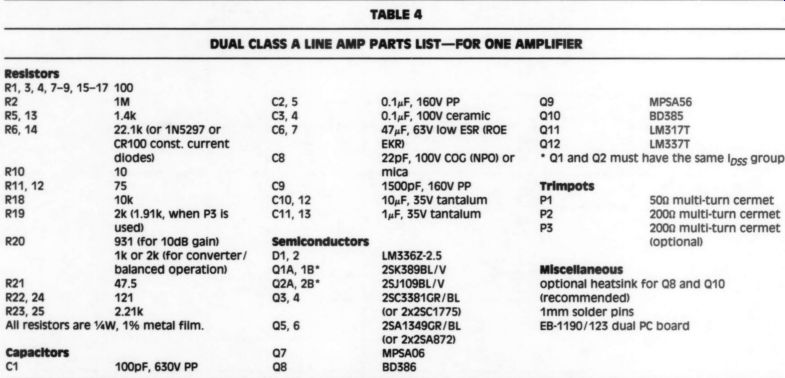
TABLE 4--DUAL CLASS A LINE AMP -- PARTS LIST--FOR ONE AMPLIFIER: Miscellaneous optional heatsink for Q8 and Q10 (recommended) 1mm solder pins, dual PC board
However, I have included separate regulators for each amplifier. If you use the two halves as a single-ended line amp for left and right channel in a normal preamp, you can operate the two amps as completely independent units with separate regulators. In the case of using the two halves for one channel in a balanced amplifier, you have the choice of using a single regulator for both amps or separate ones for each.
---------
Kits
The EB-1190/122, the EB-990/120, and the EB-489/104 are each sold as a pair for normal stereo operation and the EB-1190/123 as a dual amplifier for normal stereo operation. The EB 990/120 is also sold in four units for balanced operation. For the EB-1190/ 123, two boards are needed for converter/balanced operation (see application information).
Kits include drilled PC boards, all resistors, capacitors, and semiconductors. Components are packed in plastic bags and are marked with component number or value. We reserve the right to substitute components of equal quality.
The EB-1190/122, the EB-489/104, the EB-489/104, and the EB-1190/123 designs are the property of Erno Borbely. Commercial use of the design is not authorized without a license agreement.
---------------
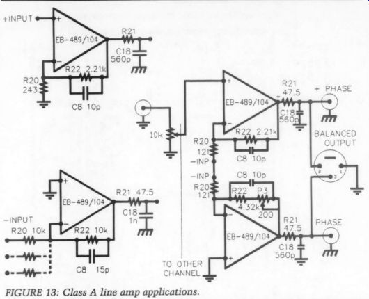
FIGURE 13
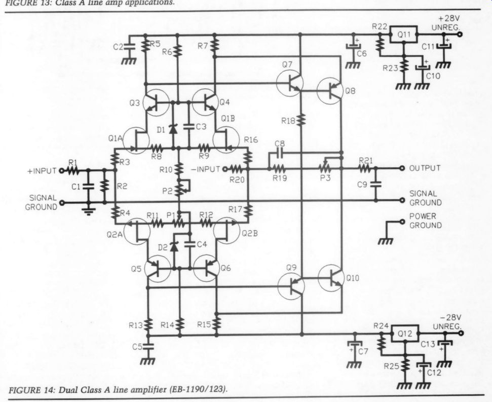
FIGURE 14: Dual Class A line amplifier.
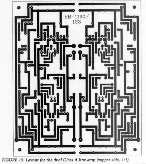
Fig. 15
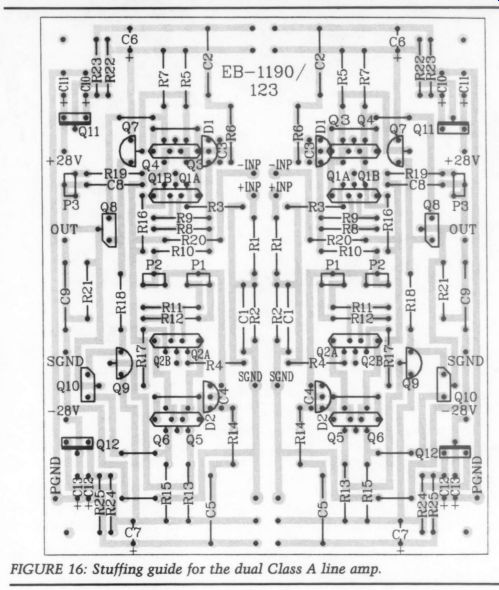
FIGURE 16: Stuffing guide for the dual Class A line amp.
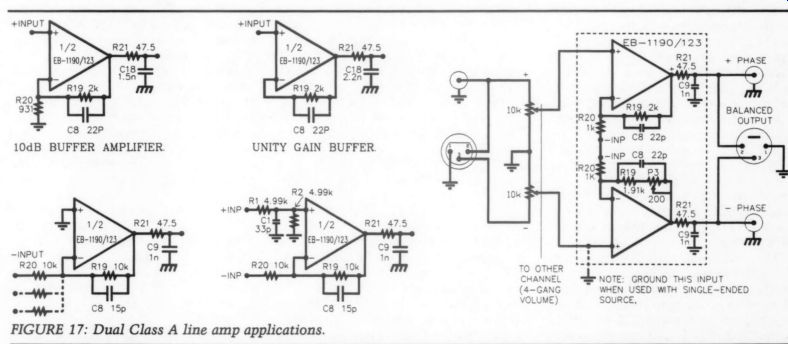
FIGURE 17.
To save a bit of board real-estate, I made the layout for only one type of input FET, the monolithic 2SK389/ 25J109. I kept open the possibility of using two types of cascode transistors: the 2SA1349/2SC3381 monolithic duals or the 2SA872/2SC1775 singles. Make sure you consult the pinouts when in stalling the single devices. The second stage is using the BD385/BD386 TO 202 transistors as in the original circuit.
I recommend putting a common or separate heatsink on the output devices.
SETUP PROCEDURES
If possible, test each amplifier module separately before installing it in the chassis. This simplifies measurements, adjustments, and component changes if they are necessary. If you have access to a scope, connect it to the output of the module and check whether radio frequency (RF) oscillations are present. If you have complete audio instrumentation in your workshop, perform the usual gain, frequency response, noise, total harmonic distortion (THD), and intermodulation distortion (IM) measurements. Inputs should be shorted under DC measurements/ adjustments.
All-Cascode RIAA-1 V.3 Before testing, set P1 to mid-position and P2 to minimum resistance value.
Short - INP to signal ground at the in put and short signal ground to power supply ground at the output. If the servo amp Q8 is socketed, don't install it yet.
Connect + 28V unregulated supply to the module and carry out the following measurements/ adjustments:
1. Check the supply voltage after the regulators Q20/Q21 (for example, across C19/C22), which should be + 24V. Check the voltage after the regulators Q7/Q9 (for example, across C7/ C8); it should be *=15V.
2. Check the offset at the output with a DC millivoltmeter and adjust P1 for OV. Install Q8 and observe the offset at the output. After about two minutes, it should go down to about 2mV.
3. Check the total current consumption of the module by inserting an am meter in series with one of the supply lines. Using P2, adjust total supply cur rent to 70-75mA. This will allow you to operate in Class A for all practical signal levels in the high-gain position.
The low-gain position requires approximately 130mA for Class A operation.
It is necessary to heatsink Q14 and Q18.
You can also use a common heatsink for all four output devices as indicated on the stuffing guide.
Class A RIAA-2 V.3 Before testing, set P1 to mid-position and P2 to maximum resistance value.
Short signal ground to power supply ground at the output. If the servo amp Q12 is socketed, don't install it yet.
Connect 28V unregulated supply to the module and carry out the following measurements/adjustments:
1. Check the supply voltage after the regulators Q14/Q15 (for example, across C12/C13), which should be + 24V. Check the voltage after the regulators Q11/Q13 (for example, across C6/C11); it should be +15V.
2. Connect a voltmeter across R5 (or R7) and adjust the voltage drop to 2.8 3V using P2. If you can't adjust it up to 2.8V, short out R10 (22.1). If the voltage drop is more than 3V with P2 set to maximum, replace R10 = 22.1 with 1009.
3. Check the offset at the output with a DC millivoltmeter and adjust P1 for OV. Install Q12 and observe the off set at the output. After about two minutes, it should go down to about 2mV.
4. RIAA accuracy should be tested together with the RIAA-1 board.
Class A Line Amp Before testing, set P1 to mid-position and P2 to maximum resistance value.
Connect the -INP to signal ground when used in noninverting configuration or the + INP to signal ground when used in inverting mode. Short signal ground to power supply ground at the output. If the servo amp Q12 is socketed, don't install it yet. Connect + 28V unregulated supply to the module and carry out the following measurements/ adjustments:
1. Check the supply voltage after the regulators Q14/Q15 (for example, across C12/C13), which should be + 24V. Check the voltage after the regulators Q11/Q13 (for example, across C6/C11); it should be +15V.
2. Connect a voltmeter across R5 (or R7) and adjust the voltage drop to 2.8 3V using P2. If you can't adjust it up to 2.8V, short out R10 (10). If the voltage drop is more than 3V with P2 set to maximum, replace R10 = 10 with 100 ohm.
3. Check the offset at the output with a DC millivoltmeter and adjust P1 for 0V. Install Q12 and observe the off set at the output. After about two minutes, it should go down to about 2mV.
4. For adjusting the gain accurately, install P3. Connect a 1kHz audio oscillator to the input and set the input level to 0.5V RMS. Measure the output voltage with an audio millivoltmeter and using P3, adjust it to 5V RMS (gain is set to + 10x, noninverting mode). This adjustment is essential when using two line amps for phase reversal and is recommended for balanced operation.
Dual Class A Line Amp
Before testing, set P1 to mid-position and P2 to maximum. If used in noninverting configuration, short -INP to signal ground. When the amp is operating in inverting configuration, the + INP has to be connected to signal ground.
Short signal ground to power supply ground at the output. Connect 28V unregulated supply to the module and perform the following measurements/adjustments:
1. Check the supply voltage after the regulators Q11/Q12 (for example, across C6/C7), which should be +24V.
2. Connect a voltmeter across R5 (or R7) and adjust the voltage drop to 2.8 3V using P2. If you can't adjust it up to 2.8V, short out R10 (10). If the voltage drop is more than 3V with P2 set to maximum, replace R10 = 10 with 100 ohm.
3. Check the offset at the output with a DC millivoltmeter and adjust P1 for 0V.
4. For adjusting the gain accurately, install P3. Assuming you have selected the 10dB gain option, connect a 1kHz audio oscillator to the input and set the input level to 0dB. Measure the output voltage with an audio millivoltmeter and using P3, adjust it to + 10dB.
I hope you will have fun building these modules and enjoy listening to music. Please report your findings through TAA. We are all learning from the feedback you are giving us. Good luck with your projects.
ACKNOWLEDGMENT: Mr. Dick Nelson of Simi Valley, California, proofread and cross-checked all schematics, component lists, and stuffing guides. He found a number of inconsistencies and some plain faults. I very much appreciate his help and hope he will have fun building these modules as well.
--------------------
++++++++++++++++
Also see:
A SIMPLE CURVE TRACER--Part II, By Erno Borbely