FEEDFORWARD ERROR CANCELLATION: APPLICATIONS AND MEASUREMENTS
BY RONALD M. BAUMAN
ABOUT THE AUTHOR: The author is an electrical engineer working on advanced radio communication systems. He has been involved in the design of high dynamic range communication systems and subsystems, such as wideband feedforward RF power amplifiers, active antennas, feedforward RF preamplifiers, adaptive interference cancellers, and wideband RF system architectures for enhancing naval shipboard communication and solving its concomitant electromagnetic interference problems. As an amateur audio designer, he finds many parallels between RF and audio design solutions, using techniques he learns from one to cross fertilize the other. The author lives in Washington, DC with his wife, Marcia, and sons, Marcus and Mitchell.
---------------
IN THE FIRST ARTICLE in this series, I reviewed the basic theory of feedforward error cancellation and told you how to apply it to a line amplifier. In this article, I will explain how to use the right components to implement the line amplifier, show the results of some distortion-cancelling experiments, and develop a complete line-amplifier design, including a parts list. I will describe its layout and how to adjust it, and tell you how it sounds.
OUTPUT
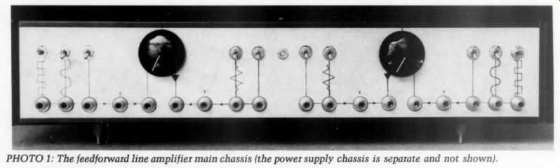
PHOTO 1: The feedforward line amplifier main chassis (the power supply chassis is separate and not shown).
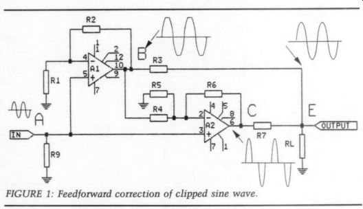
FIG. 1
Introduction
Ears are remarkable instruments, having a combination of sensitivity and instantaneous dynamic range of at least 130dB, which few, if any, electronic test instruments can equal. They hear things in reproduced music, usually distortions of some kind, which we have not yet learned to measure. Better ‘test instrumentation' may be the reason ‘golden ears ’ have led the way in improving the sound of high-fidelity equipment over the past two decades.
Among the many things we have learned is that standard harmonic and intermodulation test results are poor predictors of sound quality and that it takes more than good or clever circuit topology to produce hi-fi sound. The right kinds of passive components are just as important. Cables and wires, capacitors, switches, printed circuit (PC) boards, and other passive components make a significant difference in sound quality. These points have been made elegantly before, but are worth reinforcing because of our predisposition to underestimate their importance.
The problem with using your ear as a test instrument is that it is qualitative rather than quantitative. As such, ears are good for determining which components sound different or better than others. We hear that tubes sound better than transistors, that one type of speaker cable sounds better than an other, that a particular brand of potentiometer sounds better than others, that silver-plated connectors sound better than gold-plated ones, which sound better than copper-plated ones (or vice versa), that oxygen-free copper sounds better than standard copper, that toroidal transformers sound better than "E" types, and so on. Why does one type of component sound better than another? Little in the way of published work appears to answer that question.
The lack of hard science to support component selection leads to the necessity to perform comparative testing of components to determine which one sounds best-a slow and costly process.
Few of us have the time and resources to make the hundreds of comparisons needed to sort out the best components and combinations of components. In any case, rarely do these comparisons lead to quantitative design rules.
A notable exception is the work of Jung and Marsh on dielectric absorption and diode effects in capacitors. [5] Their work has led to the general design rule that low dielectric absorption capacitors sound better than high dielectric absorption types. If the sound of capacitors is affected, it is reasonable to assume that dielectric materials will also affect the sound of other components with implicit capacitance-cables, hookup wires, printed circuit boards, and transformers. However, I am not aware of work that addresses the effect of dielectric material on the sound of components other than lumped capacitors. In general, design rules for choosing most of our hi-fi system components seem to be lacking.
We need a compendium of work, including the work of Jung and Marsh on capacitors and an extension of the work Ruck has done on connectors and wires, that establishes design rules to help us select components. Until this is accomplished, we are left to trial-and error techniques.
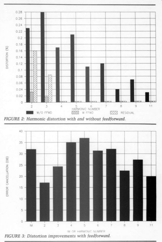
FIGURE 2; FIGURE 3: Distortion improvements with feedforward.
I have performed limited comparative testing on several types of interconnect and speaker cables to determine which ones sound best. The tests didn't establish comprehensive design rules, but their results, quasi-scientific though they are, influenced at least some of my passive component choices.
I had read that some interconnect and speaker cables sound better than others, but I had not conducted my own comparative experiments to deter mine how significant the differences were. (I had also heard that some of these cables were quite expensive- hundreds of dollars per foot.) More appears to have been written about speaker cable than low-level interconnects. For example, an article by Pass' found that some amplifiers oscillated with high capacitance speaker cables, that the differences between cables were more apparent for long cables, and that a correlation appeared to exist be tween pulse response and sound. Pass also discovered that heavier (thicker) cables paid off in better bass response and midrange definition.
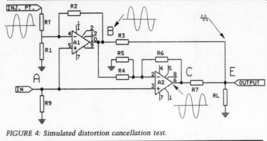
FIGURE 4: Simulated distortion cancellation test.
An engineering analysis by Greiner on nine types of cable found that for 10 meter lengths little engineering evidence existed to recommend one over another. He recommends low-resistance twisted pairs-making sure connections are tight at both ends-and minimizing cable length.
[Both Pass' and Greiner's studies were done ten years ago.-Ed.]
Based on Pass' and Greiner's findings, I reasoned I could finesse the ‘sound-of speaker-cable ’ problem by placing my power amplifiers immediately behind the speakers to reduce the speaker cable length to 3'. I used 16-gauge zip cord as my baseline speaker cable.
After comparative tests with several other types of speaker wire, I could hear significant differences in sound quality even with 3' cables. The improvement in sound of the better cables was apparent not only at the low- and high frequency extremes, but throughout the entire frequency range in the form of the three ‘Ds ’-more dynamics, detail, and delineation of instruments.
In short, the sound was closer to live music. My initial reasoning that short leads would negate cable sound differences had been wrong.
As a result of these tests, I have concluded that the engineering analyses of speaker cables fail to account for the parameters that most significantly affect their sound. I don't know what all those parameters are, but they must include the dielectric material of the insulators, the quality of the conductor, and its configuration. Consistent with Ruck's analysis, stranded copper cables did not sound as good as solid cable in the tests.
I must stress again that my tests were not scientific. Few of the many potential variables were controlled, and I used only one speaker system for the test.? Still, the differences in the sound of the cables were not subtle: they were immediately and readily apparent. I obtained similar results with interconnects: differences were apparent even for short lengths (less than a foot) and good dielectrics and solid wire sounded better.
I have heard significant improvements in overall sound quality from paralleling or replacing electrolytic and ceramic filtering, coupling, and bypass capacitors with high-quality Teflon, polystyrene, or polypropylene capacitors in new and used audio equipment.
Even components like switches can make a difference in sound quality, so you should also choose them carefully.
How does this relate to a feedforward line amplifier? To justify the heroic de sign measures I have taken to eliminate or reduce the number of switches, electrolytic capacitors, and PC boards in the signal path. A poor component can significantly degrade the sound of an otherwise fine-sounding amplifier.
Thus, choosing the right component ...
---------------
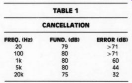
TABLE 1--CANCELLATION
--------------------
... can be as important to good sound as circuit topology.
To refocus on feedforward error cancellation, I will first share some measurements I made on a feedforward line amplifier to show how powerful the technique is at cancelling harmonic and intermodulation distortion. (Although harmonic and intermodulation distortion are not strong indicators of sound quality, the ability to cancel these steady-state types of distortion should be indicative of the circuit's ability to cancel other types of additive distortion.
Erno Borbely ’s multi-tone IM test (could be used here.) Then I will plunge into the line amplifier circuit and its implementation details.
Measurements
Figure 1 shows the line amplifier and the waveforms that appear at significant points in the circuit under conditions of mild sinusoidal overdrive (clipping) of the main amplifier, Al. These wave forms are based on an actual circuit's oscilloscope waveforms. A sinusoid is coupled to the input (port A) of the feed forward amplifier. The waveform at the output of Al (port B) shows clipping.
The waveform at the output of the error amplifier, A2 (port C), is the amplified error signal which, when combined with the clipped output of Al at port E, restores the signal to nearly its original shape. To quantify the improvement, I took harmonic and intermodulation distortion data on the circuit with and without the error amplifier connected.
The excitation is a 1kHz sinewave adjusted in amplitude so the main amplifier output is at the onset of clipping (about 0.5dB compression of the waveform). Figure 2 shows the results of the harmonic distortion test. The three bars clustered about the harmonic numbers show the residual distortion of the test instrumentation, the harmonic distortion of the main amplifier without feed forward correction, and the harmonic distortion of the complete feedforward amplifier.
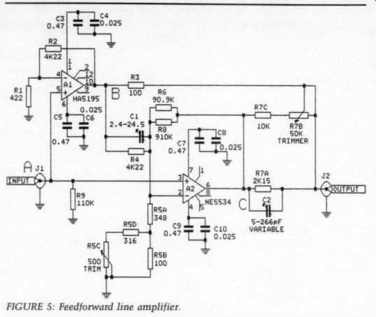
FIGURE 5: Feedforward line amplifier.
The data needs some explanation.
The wave amplifier (a trusty HP 302A) used to examine each harmonic selectively is limited to a dynamic range of 70dB. The dynamic range of the main amplifier under clipping conditions, however, is at least 50dB and that of the complete feedforward amplifier at least 80dB. Thus, the instrumentation does not have enough dynamic range to show the feedforward amplifier's real improvement. I derived harmonics smaller than the test instrument residual by taking the square root of the difference between the squared residual and the squared residual plus distortion reading. You could significantly improve the dynamic range of the test instrumentation by using notch filters or more exotic techniques, but I think the data illustrates that feedforward is per forming its job of cancelling undesirable harmonics.
I performed the intermodulation (IM) tests (using a Heathkit IM 48) under the same clipping conditions as for the harmonic distortion tests. For the IM tests, I adjusted the 60Hz and 6.15kHz test tones of the IM 48 for equal amplitude. Figure 3 shows the combined IM test and harmonic distortion test results in terms of decibel improvement with feedforward. (The leftmost bar is the IM improvement, the others are the improvement in harmonic distortion based on the data in Fig. 2.) The results represent minimum improvement because of limitations in my test instrumentation's dynamic range.
To help overcome this limitation, I devised a measurement trick-avoid injecting the test signal into the common ports of the main and error amplifiers, which in Fig. 4 are the noninverting input ports. Therefore, I modified the basic circuit so I could inject a simulated error signal into Al's inverting in put. As I can make the error signal quite large (relative to normal distortion errors, which are in the millivolt to microvolt range), I can overcome my current test instrumentation's dynamic range limitations. Figure 4 shows the modified circuit along with the cancellation test's representative waveforms.
With no common reference signal to cancel its counterpart, the error amplifier treats the main amplifier's output as if it were an error signal. Ideally, then, port E in Fig. 4 should have no output signal. Table 1 shows the test results.
------------
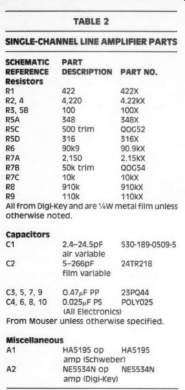
TABLE 2
SCHEMATIC REFERENCE
Resistors R1 422 R2, 4 4,220 R3, 5B 100 R5A 348 R5C 500 trim RSD 316 R6 90k9 R7A 2,150 R7B 50k trim R7C 10k R8 910k 910kX R9 110k 110kX All from Digi-Key and are 4W metal film unless otherwise noted.
PART DESCRIPTION
PART NO.
422X 4.22kX 100X 348X QO0G52 316X 90.9kX 2.15kX QOG54 10kX Capacitors C1 2.4-24.5pF air variable C2 5-266pF film variable 530-189-0509-5 24TR218 3, 5, 7, 23PQ44 4,6, 8, 9 0.47uF PP 1 POLY025 0 0.025yF PS (All Electronics)
From Mouser unless otherwise specified.
Miscellaneous
A1 HA5195 op HA5195 amp (Schweber) A2 NE5534N op NES5534N amp (Digi-Key)
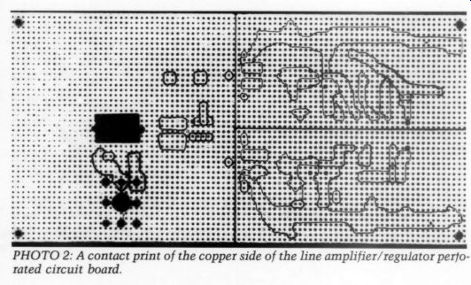
PHOTO 2: A contact print of the copper side of the line amplifier/ regulator perforated circuit board.
FIGURE 6: Regulators. (below)
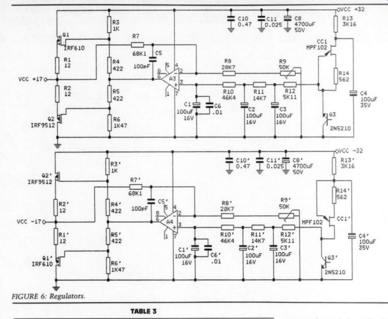
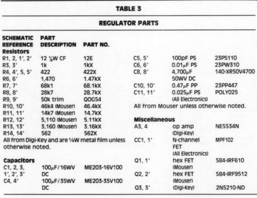
TABLE 3 REGULATOR PARTS
-------------
The first column in Table 1 is the simulated distortion signal's frequency.
The second and third columns are the cancellation capability of the error isolation loop and of the simulated error signal, respectively. Thus, I expect at least 32dB cancellation of distortion in normal operation.
Happily, the results of the IM test, shown in Fig. 3, correlate well with the simulated error cancellation data in Table 1. IM cancellation is only 32dB in Fig. 3 because significant IM products are clustered about the third harmonic of the higher IM test tone (18.45kHz), putting them near 20kHz where cancellation (Table 1) in this circuit is limited to 32dB. Although the error-isolation loop was phase compensated to a first order to achieve cancellation of 75dB and greater, as in Table 1, the error-cancelling loop was not (be cause I lacked the variable capacitor needed for phase compensation at the time I took the data).
Line Amplifier
The line amplifier schematic is shown in Fig. 1. I explained this circuit's operation in the first article of this series.' Notice the variable components (R5C, R7B, C1, and C2). They are used to balance the error-isolation and error-cancelling loops.
Variable capacitors are seldom seen in audio amplifiers, but here they are included to first-order phase compensate the loops over the audio band. You can eliminate C1 and 2, but this will reduce cancellation by several orders of magnitude at higher frequencies.
Balancing the loops requires precise setting of R5C and 7B. To ease the adjustment, I implemented R7 and 5 of Fig. 1 as three or four resistors, with one as the variable component. This arrangement allows relatively large potentiometer wiper motion for little change in net resistance.
C3-10 are included as high-frequency bypasses for the op amps' power leads.
At each bypass point, a parallel combination of a polypropylene and polystyrene capacitor is used. Teflon capacitors would have been a better choice, but they are approximately ten times as costly and hard to find. A less costly compromise is a high value polystyrene without the parallel polypropylene.
However, these are also costly and as hard to find as Teflon. If you can find and afford either type, use them.
Regulators
Schematics of the positive and negative 17V regulators are shown in Fig. 6. I used independent, rather than tracking, regulators because I think they sound better. A possible explanation may be that they better maintain stable bias conditions for asymmetrical signals. After all, music waveforms are, over short periods, usually not symmetrical.
The reference voltage for the regulator is provided by Q3, a transistor connected as a temperature-compensated zener. This will be different for each transistor and varies between 6 and 9V.
For any given transistor at a constant current, however, the reference voltage varies little with temperature. R9 allows adjustment of the regulator out put voltage to 17V.
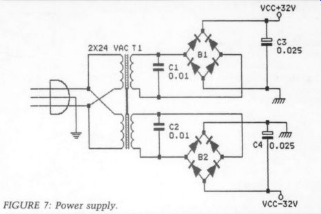
FIGURE 7: Power supply.
--------------
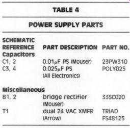
TABLE 4 POWER SUPPLY PARTS
SCHEMATIC REFERENCE
Capacitors C1, 2 C3. 4 PART DESCRIPTION PART NO.
0.01 uF PS (Mouser)
0.025 uF PS (All Electronics)
23PW310 POLY025
Miscellaneous B1, 2 bridge rectifier (Mouser)
dual 24 VAC XMFR (Arrow) 33SC020 TRIAD FS48125
-----------------
Q3 is supplied a constant current by CC1, a FET connected for that purpose.
The C4/R13 network provides first order filtering of line voltage ripple and noise. R13 also assures that CC1 operates within its safe voltage limit. The network of R10/R12 and C1/C3 pro vides a three-pole filter that attenuates the noise of the reference voltage and any residual line noise and ripple by at least 120dB at audio frequencies.
As previously mentioned, electrolytic capacitors degrade sound quality. Therefore, I try to eliminate them from the direct signal path. The tradeoff this circuit makes is to substitute wideband, low-impedance regulators for electrolytic capacitors. For this to be successful, the regulator must be able to source and sink current symmetrically. There fore, I chose a push-pull audio amplifier topology for these regulators. In this design, the regulator operates with a closed-loop bandwidth covering the full audio spectrum.
The choice of the regulator output devices is particularly important be cause they have no electrolytic filter capacitors to shunt distortion the regulator may produce. To be sure, I used polystyrenes and polypropylenes to provide high-frequency filtering of the line amplifier's op amps, but the line amplifier depends on the regulator's low output impedance to return the signal currents to the power supply. I chose MOSFETs rather than transistors as the regulator output devices because they exhibit a more linear change in trans conductance as the load current changes and I think they sound better than transistors in this circuit. R1 and 2 protect the MOSFETs from short-circuits. No other protection is provided other than a fuse in the power supply.
Power Supply
The power supply schematic (Fig. 7), in keeping with the design philosophy of independent plus and minus bias volt ages, employs two transformer windings and two full-wave bridges to sup ply 32V to each regulator. All circuit grounds are connected to a single point on the line amplifier chassis. The power supply is in a remote chassis to minimize coupling of its stray magnetic fields with the line amplifier's signal processing circuitry. The power supply chassis is connected to power line ground and, through a wire, to the single point ground in the line amplifier chassis.
Input Selector
The line amplifier can act as the switching center for the system in which it is used. Unfortunately, every switch I have tested introduces noticeable de gradation in sound quality-some more than others. The more you improve your system, the more things like switch degradation become apparent.
The Best Switch Is No Switch
Given that switches degrade sound quality, the input selector design should minimize or eliminate switches in the signal path if possible. The input selector circuit I have designed can eliminate switches in the signal path. Figures 8a and 8b show two variations of the design.
In Fig. 8a, the first two inputs are connected through fixed resistors to the upper arm of the volume control potentiometer, R4. Thus, no switch contacts'? are in the signal paths of either the phono or CD inputs. A signal source is selected by ‘un-shorting ’ its ground connections. For example, to select the phono source, open switches S1A and S1B as shown in Fig. 8a.
You could also implement the switching arrangement with a rotary switch, but I chose to use individual, silver-plated, copper-contact toggle switches instead. Source selection is, therefore, a little unusual in that you must remember to ‘unselect ’ a previous source before selecting a new one.
On the other hand, you can use this arrangement as a crude mixer-crude in that it lacks individual potentiometers for each source.
This ‘switchless ’ input selector comes at a price-insertion loss and relatively low input impedance. The insertion loss is plotted in Fig. 9 for a selected range of circuit components; it shows values of R3 that minimize insertion loss.
The exact equation for the input se lector insertion loss is:
20 x LOGIN + 2 x R1/R4 + R3/R4
+ 2(N - 1) x R1/R3)
Where R1, 2, and 3 are as shown in Fig. 8a and R4 is the resistance of potentiometer R4 loaded by the input resistance of the line amplifier. I have assumed a value of 75k for R4 and N is the number of switchless inputs. I have also assumed R2 = R1.
The more ‘switchless ’ sources you have, the greater the insertion loss. For example, Fig. 9 shows approximately 7dB insertion loss for two switchless sources and approximately 15dB for five.
As the line amplifier has a gain of 20dB, the switchless configuration for two sources leaves 13dB of net gain to handle weak sources.
To select the values of R1-4, I made some assumptions. I selected R4, the volume control, first. It is the only variable resistor in the signal path, so it must sound good. In the absence of any first-hand test data on the sound of various potentiometers, I selected a dual ALPS for each channel for this application. CERMET or carbon or plastic film are other alternatives.
Figure 9 gives us guidance for selecting the value of R1. The smaller R1 is, the smaller the insertion loss. Since the insertion loss is not strongly dependent on R1, we can make it large enough not to short or overload the source. I chose 604 for R1 and 2. Assuming R2 = R1, the optimum value (in terms of minimizing insertion loss) of R3 is:
√ [2 x (N = 1) x R1 x R4]
Figure 10 plots the optimum value of R3 as R1 varies for a fixed value of R4 (75 k-Ohm). With the assumptions and choices I have made, the optimum value for R3 is 9.518 k-Ohm. The closest standard value 1% resistor is 9.53k-ohm.
You may wish to make other trade offs between the number of ‘switch less ’ sources, the number of conventional series switched sources, and gain. The design guidance given in this and the previous article allows you to make almost any combination of trade offs. The one I implemented, for example, is shown in Fig. 8b.
In this variation, the sources are grouped into two sets: the active set, which has two inputs, only one of which is switchless, uses the line amplifier for added amplification; in the passive set, the sources are switched to a potentiometer (the other half of the dual ALPs control), the wiper of which is the output. This arrangement re quires manual patching of the passive or active group of sources to the power amplifier. Tape outputs are available at the top of each potentiometer and pro vide additional patching options.
Line Amp/Regulator and Power Supply Boards
Photo 2 is a contact print of the copper side of the line amplifier/regulator printed circuit board. Notice that white is copper and black is substrate or a hole. The board has a matrix of holes on 1/10" centers. Thus, you can repro duce the etching by counting holes and following the etch lines.
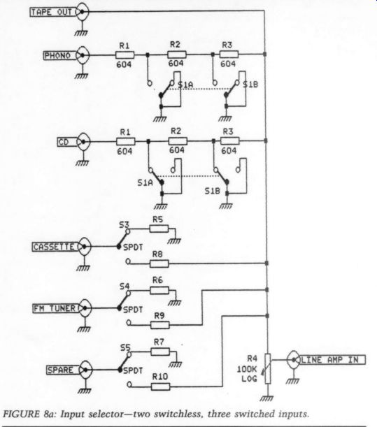
FIGURE 8a: Input selector-two switchless, three switched inputs.
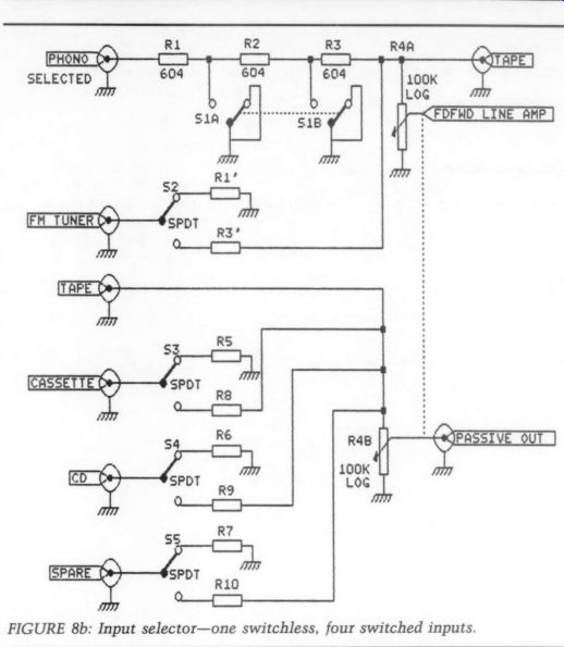
FIGURE 8b: Input selector-one switchless, four switched inputs.
Notice also the three distinct rectangular foil sections: for the line amplifier, positive regulator, and negative regulator. With this layout, each section is isolated from the other and can be connected separately to a single chassis ground point.
For those components in the main signal path, the largest section of the board is used only as a ground plane and mounting board. Photos 3 and 4 show the top and bottom of the completed circuit board. Note the point-to point wiring on the ground plane side of the board. The few islands of copper are for the error-amplifier components.
The regulators use islands of copper rather than small traces for interconnecting and mounting components.
-------------
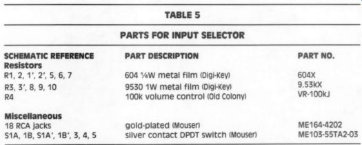
TABLE 5--PARTS FOR INPUT SELECTOR
SCHEMATIC REFERENCE
Resistors RL2 1,2. SRT R3,3', 8,910
Miscellaneous 18 RCA jacks S1A, 1B, S1A', 1B', 3,4, 5
PART DESCRIPTION
604 WW metal film (Digi-Key) 9530 1W metal film (Digi-Key) R4 100k volume control (Old Colony) gold-plated (Mouser) silver contact DPDT switch (Mouser)
PART NO.
604X 9.53kX VR-100kJ ME164-4202 ME103-55TA2-03
--------------------
This provides a large ground plane on the interconnection side of the board.
Thus, the electric fields between the ground plane and the circuitry tend to be immersed in air rather than in the paper-epoxy dielectric on the top of the board.
The power supply board is double sided. The ground planes on both sides are connected and grounded to the isolated power supply chassis. A single power supply chassis contains a trans former and two full-wave bridges for each channel. The main filter capacitors are located on the regulator boards.
Grounding Scheme
Figure 11 shows the feedforward line amplifier grounding scheme. It is important to follow this diagram to avoid ground loops. All inputs and outputs are located in a row along the bottom of the front panel, with switches immediately above them. The single point ground chassis connection is located on the vertical center line of the front. This layout minimizes the length of most internal grounding wires.
Wires from the power supply are connected to banana jacks located in a row across the rear of the main chassis. All power supply grounds are carried from these jacks to the single point ground on the front panel.
Wiring and Chassis
The wire types I chose are based primarily on the results of extensive listening tests of interconnect wires, in which one type of wire was substituted for another.
As a result of these tests, I have concluded that solid wire is better than stranded. Therefore, no stranded wiring is used in any portion of the line amplifier, including the AC cord. I used Tefzel, 28-gauge silver-plated OFHC wire (readily available from several sources) for all power supply grounds and point-to-point supply wiring, and 20-gauge solid Teflon for the AC cord.
I used 30-gauge wire for all signal leads and signal grounds. Fine-gauge OFLC wire would have been a better choice, but I have not found a supplier for it.
If you can find either, copper or brass is a good choice for the chassis material. However, aluminum and steel are the only readily available chassis materials, although neither is ideal as either can produce intermodulation distortion. The distortion mechanisms are quite different for aluminum and steel, 4 and I'm not sure which is better for this application. Primarily because it is easy to work with, I chose an aluminum chassis. 5 The single-point grounding scheme tends to minimize chassis currents, and consequently intermodulation distortion, but some currents will always be ...
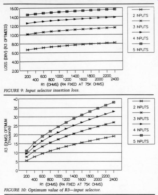
FIGURE 9: Input selector insertion loss.
FIGURE 10: Optimum value of R3-input selector.
-------------
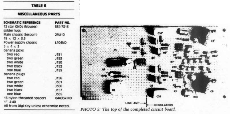
TABLE 6
MISCELLANEOUS PARTS
SCHEMATIC REFERENCE
12 star GNDs (Mouser) solder lugs Main chassis (Sescom) 19 x 12 x 35 Power supply chassis Sx4x3 banana jacks two red two green two white two black one blue banana plugs two red two green two white two black one blue 16 nylon threaded spacers 1", 4-40 All from Digi-Key unless otherwise noted.
PART NO.
534-7313 2RU10 L104ND J151 J153 J150 J152 J155 J156 J361 J360 J157 J365 8440Ck-ND
-------------------------
PHOTO 3: The top of the completed circuit board.
To access C2 on both line amplifier boards, drill holes in the bottom panel of the chassis large enough to accommodate an insulated screwdriver.
Parts List
I tried to reinforce the notion in the introduction to this article that the right components are essential to good sound.
Given that a particular component can affect an amplifier's sound, the listing of all components becomes essential if the sound of a given design is to be reproduced.
Adjustments
Check all boards for shorts, wiring, and stuffing errors and the like. The input selector switch and volume control are hand-wired to the input sockets and line amplifier boards. If you use the Sescom chassis, the front panel is re movable, making it easy to wire the in puts, outputs, and volume controls as per Fig. 8a or 8b before assembling the chassis.
Install the left and right line amplifier/regulator boards in the chassis.
Then install the front panel and finally the rear. Follow the grounding scheme in Fig. 11 and be sure no inadvertent connections are made from the board to the chassis. I used nylon standoffs to insulate the boards from the chassis.
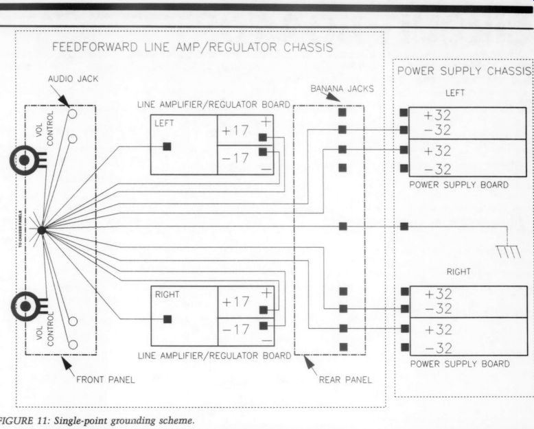
FIGURE 11: Single-point grounding scheme.
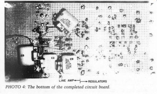
PHOTO 4: The bottom of the completed circuit board.
Use Teflon standoffs if you can find them. Check the power supply to be sure its outputs are +32V DC before interconnecting them to the main chassis through banana plugs.
Assuming the power supply and other boards are working properly, the first adjustment is to set the regulators on each line amplifier board. Remove the top panel from the chassis to gain ac cess to all adjustable components except C2, which is accessible from the bottom panel.
Before turning on power, however, remove A1 and 2 from both line amplifier boards. Now connect the power supply to the line amplifier chassis using banana plugs. Turn on the power and adjust R9 and R9' (Fig. 6 and Photo 3) on each board for outputs of plus and minus 17V DC supplies, respectively.
I installed small pins through the PC board to mount R1, 2 and R1, 2 at the output of each regulator (Photo 3).
These pins are accessible from the top of the board for easy connection to a voltmeter. The regulated output volt ages will drift very little with warmup.
After the 17V levels are set, turn off the power, reinstall A1 and 2 on both line amplifier boards, then turn on the power again and let the line amplifier warm up.
The following procedure balances the error-isolation loop. Connect a 1V RMS 20Hz sine wave to the right phono in put and select it while de-selecting all other inputs. Adjust the volume control for a 5V RMS signal at the line amplifier output jack. Connect a high-impedance probe of an oscilloscope or sensitive voltmeter to the output of A2 (port C in Fig. 5 and Photo 3). Adjust R5C for a null indication at port C. The residual signal at port C will be a few millivolts.
Now change the frequency to 10kHz.
Adjust C1 for a null indication. The residual signal at 10kHz will be several millivolts. Repeat the nulling procedure once more, using a 20Hz signal to ad just R5C and a 10kHz signal to adjust C1. Use an insulated screwdriver or a plastic screwdriver to adjust C1.
The best way to adjust the error-cancellation loop is to use an IM or harmonic distortion meter with the input connected to the right channel phono input (as above) and the output taken from the line amplifier output jack. If you are using a harmonic distortion meter, adjust the frequency to 3.333kHz so the third harmonic falls at 10kHz.
To get any appreciable reading on the distortion meter, adjust the signal source amplitude so the signal at point B just begins to clip, corresponding to approximately 2% IM or harmonic distortion. Referring to Fig. 5 and Photo 3, adjust R7B for a null in the distortion reading. Also, adjust C2, which is accessible from the bottom of the chassis, for a null indication. Repeat the procedures for adjusting R7B and C2.
This completes the adjustments of the right channel. Repeat this procedure for the left channel. Once made, these settings are stable for several years if performed on fully warmed up amplifiers.
The Sound
I built a feedforward line amplifier years ago using the same topology and op amps described in this article, but with out the benefit of better wires, dielectrics, and all I have since learned about the importance of choosing or eliminating passive components. In this regard, the new line amplifier implementation scores higher in the three Ds and is more transparent and musical than the older one. For an op amp-based design, it is the best I have heard, but I have no doubt it can be improved by using a discrete design rather than op amps.
The two outputs, implemented as in Fig. 8b, allow a direct comparison of the active line amplifier with a passive patch-through. In this comparison, the passive output sounded a little, but not appreciably, better at high frequencies, but the reverse was true for low frequencies (probably because of the lower output impedance of the active circuit).
The bottom line to a listening session, for me anyway, is the ratio of exhilaration to fatigue. I would score this ratio very high, but not infinite, for the listening sessions with the new feedforward line amplifier.
In the next part of this series, I will develop the design and provide implementation details of a feedforward phono preamplifier.
REFERENCES
1. Bauman, R.M., 'Feedforward Error Cancellation, ’ TAA 4/89, p. 15.
2. Colloms, Martin, 'The Sound of Amplifiers,' TAA 3/85, p. 6.
3. Marsh, R.N., 'Dielectric Absorption in Capacitors, ’ TAA 4/80, p. 31.
4. Jung, Walt and R.N. Marsh, POOGE-2, TAA 4/81, p. 7.
5. Jung, Walt and R.N. Marsh, 'Selection of Capacitors for Optimum Performance,' Audio, February 1980.
6. Ruck, William, ‘Current Thoughts on Wire, ’ TAA 4/82, p. 22.
7. Pass, Nelson, ‘Speaker Cables: Science or Snake Oil?' SB 2/80, p. 6.
8. Greiner, R.A., "Cables and the Amp/ Speaker Interface,"' Audio, August 1989.
9. The speakers were Magneplanar Tympani 1D. I checked the amplifiers to ensure they did not oscillate with highly capacitive or inductive loads in combination with high- or low-resistive loads.
10. Electrolytic capacitors used to filter the power supply lines are in the signal path.
11. Borbely, Erno, ‘A Multi-Tone Inter modulation Meter,’ TAA 2/89, p. 7.
12. Work I began too late to include in this article shows that shunt may be preferable to series regulation.
13. Actually, the 'off' switches can pro duce distortion that couples to the volume control. However, for a switch contact resistance of 20 M-Ohm, the attenuation of switch distortion will be at least 95dB for the circuit of Fig.8a.
14. Strauss, G.H. et. al., 'Studies on the Reduction of Intermodulation Generation in Communication Systems, ’ NRL Memorandum Report 4233, July 1980.
15. The Sescom chassis has loose-fitting panels, each of which must be separately connected to the single point chassis ground to minimize aluminum-to-aluminum intermodulation products.
ACKNOWLEDGEMENTS
I am indebted to Marcia Bauman for the photographs used in this article. I also thank Dr. Pierre M. Sprey whose unrelenting pursuit of ever higher fidelity sound inspired many of the experiments on passive components reflected in this article.
---------
++++++++++++++++
Also see:
THE FIRST ARTICLE in this series