BY RON SAWYER
ELEGANT 12-TRANSISTOR phono amplifiers are not much better than two transistor circuits if their audio signal has buzzing noises caused by improper power supply grounding. Proper grounding techniques have been addressed in TAA, but at least one high-performance regulator design is shown with a less than optimum grounding technique. My first preamp projects were plagued by what I considered excessive levels of buzz/hum from the phono amp. Thermal noise (hiss) should be the dominant noise output of the phono stage.
I tried outboard and inboard power sup plies; I changed cables and connectors; I tried reversing the polarity of AC wall plugs; I experimented with the physical placements of components and cables; I applied anti-RFI remedies; I even tried tossing gold-plated RCA plugs over my left shoulder while hopping up and down on one leg during a partial eclipse of the sun-all with limited success.
So, I took a deep breath, opened a couple of reference books,** and stepped back to square one.
Re-Conceptions
While sorting out the rules of proper grounding, I abandoned my concept of a voltage regulator as a three-terminal device (input, output, and ground or reference) and came to regard it as a four terminal device (input, input/ground, output, and output/ground). A proper grounding scheme will isolate the regulator's output from disturbances occur ring on the regulator's (noisy) input side.
CHARGING CURRENT
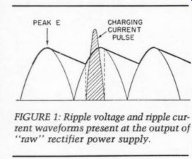
FIGURE 1: Ripple voltage and ripple cur rent waveforms present at the output of ‘raw ’ rectifier power supply.
Ripple Current
In a full-wave rectifier power supply, the filter capacitors are partially discharged and subsequently recharged at a rate of 120 times per second (on a 60Hz AC frequency line, as in the US). The filter capacitors draw the recharging cur rent in the form of sharp pulses called ripple current. Figure 1 shows the ripple voltage's waveform at the filter capacitor's output, and the shape of the associated current pulse.
The magnitude of the current pulse is limited only by the total effective source resistance of the raw power sup ply, which consists of the sum resistances of the transformer primary winding and any associated fuses, switches, and hookup wires (as reflected to the transformer secondary), plus the trans former secondary winding's resistance, the rectifier diodes' dynamic resistances, the hookup wires, and the filter capacitor's ESR.
In a real-world power supply, the ...
----------------
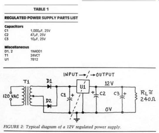
FIGURE 2: Typical diagram of a 12V regulated power supply.
TABLE 1
Capacitors
C1 1,000 uF, 25V (ov 47,F, 25V C3 10uF, 25V
Miscellaneous
D1, 2 1N4001 m 24VCT U1 7812
---------------
ABOUT THE AUTHOR: Ron Sawyer is 37 years old and a photographer by trade. He's been an audio amateur for about 15 years with TAA as the springboard. Other interests include painting and drawing. He is working on a comprehensive vacuum tube system including preamp, electronic crossover, tube-type regulated power supply, and power amps.
------------------
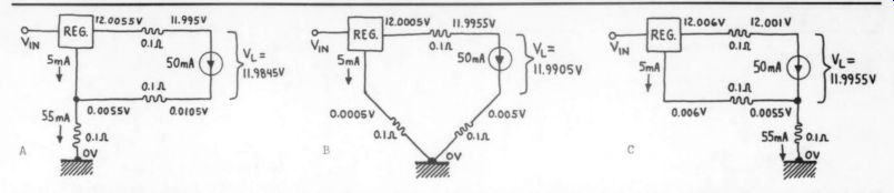
FIGURE 3: Three possible methods of grounding the output side of the voltage regulator. (C) results in less error at the load and is the preferred method. I have modeled the load after a constant-current source because the calculations result in fewer significant decimal places that must be squeezed onto the drawing notations. The load can alternately be modeled as a resistor (240 ohm); the relative merits of the three grounding methods are not altered.
----------------
... transformer secondary winding resistance is the dominant component of the raw power supply's effective source resistance. A low resistance (well-regulated) transformer combined with large filter capacitors results in large ripple current pulses being drawn from the ground bus. Such current pulses can cause significant voltage spikes to appear across the parasitic resistances in evitable with real-world wires and board traces used as ground returns. Our goal is to isolate ripple current noise from the rest of the voltage regulator and signal processing circuitry. Fortunately, the technique for doing so is extremely simple and extremely effective.
Helpful Symbols
As an aid in drawing circuit diagrams to illustrate proper grounding methods, I have found the following two symbols useful:
-|-
__
////
The single-point ground to which all system grounds are connected.
The parasitic resistance of a real world ground wire. It is actually an impedance composed of resistance and inductive reactance.
I/O Hi-Ho
Figure 2 is a typical diagram of a basic regulated power supply delivering 12V at a nominal load current of 50mA. It is in the translation from drawing to real-world wiring that the pitfalls lie.
Circuitry to the left of the dotted line will be considered the ‘input circuit ’ and to the right, the 'output circuit." Let's deal with the output side first.
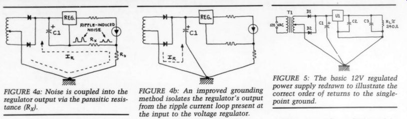
FIGURE 4a: Noise is coupled into the regulator output via the parasitic resistance (Rx).
FIGURE 4b: An improved grounding method isolates the regulator's output from the ripple current loop present at the input to the voltage regulator.
FIGURE 5: The basic 12V regulated power supply redrawn to illustrate the correct order of returns to the single point ground.
Refer to Figs. 3a, b, and c , which illustrate the three possible ways to ground the output side of the regulator.
For the sake of clarity, I omitted C2 and 3 from the following diagrams. If used, these caps should be installed as close as possible to the regulator output and the load, respectively. Assume that Vie (regulator output voltage) is 12V, I, (regulator quiescent current) is 5mA, I; (load current) is 50mA, I, (total cur rent) is I, + I; = 55mA, Rx (parasitic hookup wire resistance) is 0.12, and V, is voltage appearing at the load.
Using Ohm's law to solve for the voltage drops occurring across the parasitic hookup resistances reveals that the grounding order of Fig. 3c results in less error at the load.
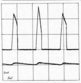
FIGURE 6: The power supply of Fig. 2 exhibits noise spikes appearing at the load when the improper grounding method is employed (upper trace). The lower trace is the result of a correct grounding method. This waveform is classic ripple voltage, and could be reduced further by the use of larger input filter caps or a regulator circuit with higher gain than the 7812-type IC. In the upper trace, the slight difference in noise spike shapes on alternate rectifier cycles is caused by asymmetry in the transformer secondary or slight differences in the dynamic characteristics of the two rectifier diodes.
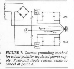
FIGURE 7
Ground Rule Number 1
The regulator output and ground terminals are connected directly to the load, and the load is returned to the single-point ground.
Turning now to the input side of the regulator, refer to Figs. 4a and 4b. Figure 4a illustrates an incorrect order of grounding; the dashed line represents the ripple current (I) path, and I have indicated where transient noise spikes caused by ripple current will appear (see Ref. 2, Fig. 6b). Figure 4b shows a preferred method, with the input filter capacitors returned directly to the single-point ground by means of a hookup wire not shared by the other elements of the system. In this way, the regulator output is effectively isolated from the ripple current path.
Ground Rule Number 2
Input filter capacitors that carry appreciable ripple current must be returned directly to the single-point chassis ground. No other system ground re turns may share any portion of this ground wire. The transformer center tap (or rectifier diode bridge) should also be returned directly to the single-point chassis ground in the same manner as the input filter caps.
Figure 5 is a redrawn diagram of the power supply of Fig. 2, showing the correct order of grounding.
To illustrate the dramatic difference proper grounding can make, I constructed the power supply of Fig. 2 with a transformer secondary resistance of about 20. I made the connections to load and ground with 12" lengths of 22 gauge stranded hookup wire. I then monitored the output noise with an AC coupled oscilloscope connected across the load (horizontal: 5mS/div. and vertical: 5mV/div.-Fig. 6). The upper trace is the result of the grounding method of Fig. 4a and the lower trace (displaced downward by one division for clarity) is the result of the grounding scheme of Fig. 4b.
Dual Polarity
In power supplies delivering dual-polarity output voltages, for example plus and minus 12V, we can enjoy the benefits of ripple current cancellation. Refer to Fig. 7, which shows the correct order of grounding for a typical dual-polarity supply. The ripple current pulses drawn by the input filter caps tend to be of equal magnitude, but opposite polarity, and tend to cancel each other at the point marked A. Complete cancellation occurs only if all elements of the sys tem, including the load, are perfectly symmetrical. Since asymmetry exists in real-world circuitry due to device variations, dual-polarity voltage regulators will still benefit from a ‘rigorously correct ’ method of grounding.
++++++++
REFERENCES
1. Marsh, R.N., 'Power Up: An Overview of Power Supply Considerations, ’ TAA 3/83, p. 16.
2. Didden, Jan, ‘A Wideband Power Supply,' TAA 1/87, p. 22.
3. The Voltage Regulator Handbook, Texas Instruments, Inc., 1977, p. 59.
4. Morrison, Ralph, Grounding and Shielding Techniques in Instrumentation, John Wiley and Sons, Inc., 1967.
++++++++
Also see: