POOGE-5: RITE OF PASSAGE FOR THE DAC960, A TWO-PART SAGA , part 1
In 1988, PHILIPS introduced a new line of products aimed at the US “high end' market, including the CD960 compact disc player and the DAC960 outboard digital-to-analog converter.
These were the first digital playback products marketed by Philips under their own name, and sold for $950 each. One year later, Philips raised the prices to $999. Prior to 1988, Philips' consumer electronics products sold in the US bore the Magnavox logo. The Magnavox products made by Philips were priced for the “mid-fi” to “budget” market, with a few low-end products also sold by Philco and Sylvania. Most of these players were manufactured in Belgium, a highly unlikely source for mass-market audio products.
Beginning with the CDB650, the Philips-based Magnavox CD players be came well known to audiophiles, since the Philips mechanisms and digital circuitry became the basis for a number of high-end CD players and do-it-your self modifications. The reasons were quite simple. The original Philips digital chip set, consisting of the now ubiquitous SAA7220P/A digital filter and TDA1541 D/A converter, was among the first chips to reveal the potential of the CD medium. The four times over-sampling circuitry, with digital filters and separate D/A converters for the two stereo channels, formed the basis for the first CD players I found even remotely listenable.
As fine as Philips' 16-bit digital circuitry was, these players shared many weaknesses which have been well documented in TAA and other audio publications. Mechanically, the CDB460, 560 and 650 left a lot to be desired with their flimsy plastic chassis and trays. If you remembered the robust construction of Philips' 14-bit players, the new generation seemed like a step backwards in this regard.
The engineers at Philips were usually excellent when it came to digital hard ware, at least at the chip level, but their understanding of high-performance analog-circuit design has been clearly suspect. The CDB650 and family-contained IC op amps considered 'high performance' in the late 1970s (typically NE5532s or LM833s), were sorely lacking when compared to the current generation of analog chips. Philips paid little attention to parts quality, often using carbon film resistors and cheap electrolytic coupling capacitors in critical locations. Although Philips' engineers designed regulated power supplies for these players, they virtually negated the benefits of regulation by putting so called “safety ” resistors in series with all of the DC supply rails, thereby raising the output impedances of the sup plies and making dynamic regulation all but impossible.
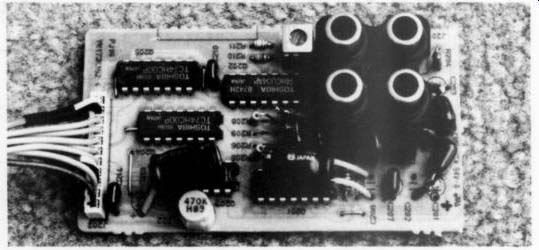
PHOTO 1: The modified PJ16 digital-input board. The HF Q bypass capacitors
lay on top of the integrated circuits.
An Outboard DAC
I've modified my own CDB650 well beyond POOGE-4 standards. I use a prototype of the Old Colony KG-5 power supply to operate the analog circuitry and D/A converter, fed by a hefty out board toroidal transformer. I've further improved the analog circuitry by changing the output buffers to Linear Technology LT1010s (biased with 33 ohm resistors) and I've changed the current to-voltage (I/V) converters to Elantec EL-2020 transimpedance amplifiers.
But, there's a limit to how much circuitry can be packed into the 650 chassis. I realized a long time ago that I'd eventually have to move to an outboard D/A converter in order to substantially improve my player's performance.
Last fall, Walt Jung asked if I'd be interested in collaborating on a DAC960 modification article for TAA. A lot of the circuitry had already been developed by Walt and his colleague Hampton Childress, but there would be more development work needed to adapt their designs to this specific project. We agreed that I would undertake the actual writing of the article and subsequent support for the project. This seemed like the next logical step for my CD playback system, so I welcomed the opportunity.
When Philips first introduced the 960-series components, I naively hoped they had recognized their previous errors, learned from the body of modification articles published on their players, and designed a new generation of high performance digital-playback gear. I later discovered Philips made a number of improvements on their previous de signs, but repeated many of the same mistakes.
-----------------
How Does It Sound?
by Wyn Palmer
'Perfect sound forever' was the promise made for the compact disc system at its introduction around 1980. Most listeners have made the transition from the LP format to CDs, however many audiophiles still insist on the ““musical ” superiority of the LP over the CD.
As a member of this ever diminishing lunatic fringe, indeed as someone who has made the move from LPs to CDs and back again, I have been de scribed (not too inaccurately) as a “raging digi-phobe ” (sic). This makes any assessment of the modifications to the DAC960 something of a two edged sword. On one side was my ad mitted predisposition to find anything to do with CDs unacceptable, and on the other was my standing as an IC de signer for Analog Devices (many of whose parts are used in the modification). So, I was determined to make the evaluation as objective as possible, at least within the framework of a purely subjective assessment (no A/B/X comparisons here!).
Anyway, having two years ago swapped my CD playback system for a large quantity of London, RCA, and Mercury stereo LPs, I had to borrow a selection of CDs and CD players/ digital processors/CD transports to make the assessment reasonable. The equipment in general was not ‘high end' (except for a new Krell CD transport which I borrowed), but I believe it would nevertheless provide a basis for comparison.
The results when listening to the control group were as anticipated. The sound of the stock CD systems was very much as I remembered. That is poor stereo imaging (the image wanders in space), little realistic dimensionality (both depth and width), a lack of warmth and ambience, with a hard string tone tending towards brightness.
On the plus side-the obvious CD benefits; well controlled, but substantial bass, low distortion-especially during heavily modulated passages--a tonal purity that is especially notice able on solo piano, and also a freedom from ticks, pops, and crackles.
Overall it was a very unmusical, un-involving, experience, and I kept finding myself longing for my familiar LP sound, and congratulating myself on how sensible I was for abandoning my CD player for a turntable.
Then I listened to the modified converter. Frankly, I was surprised. I had been promised that many of the CD playback problems would be eliminated by the design, and amazingly, those promises were largely fulfilled.
It actually reproduced a natural sound field, with convincing (and sometimes excessive) depth. The image was rock solid. Very acceptable amounts of ambience and room acoustic artifacts could be identified. Not all was perfect, however, the bass, although taut, lacked weight and fullness. It seemed to be missing some of the foundation which, in my opinion, orchestral mu sic is based. I nevertheless did not long, quite so wistfully for my LPs, and indeed found their ticks, pops and distortion more intrusive.
The question still remained: was this revelation due to the modification, or was it due to the intrinsic properties of the DAC960? A few phone calls resulted in an unmodified converter being shipped to me for comparison. The answer came very quickly- the unmodified device clearly belonged to the same fold as all the other stock CD players, the improvement was in deed due to the modifications.
Having become convinced of the quality of the modified converter, I re turned to making comparisons be tween the CD system and my cherished LP playback system. I compared a number of CDs with the LP originals, borrowing or buying the CDs when necessary.
These included:
Mercury-Respighi, The Birds, Brazilian Impressions, Dorati.
Chesky-Bizet, Symphony in C, Munch.
Mercury-Kodaly, Hary Janos Suite, Dorati.
Sheffield-Prokofiev, Romeo and Juliet-Highlights, Leinsdorf.
RCA-Prokofiev, Alexander Nevsky, Riener.
RCA-Casino Royale, Burt Bacharach.
BBC records-Enya.
RCA-Sibelius, Violin Concerto, Heifetz, Reiner.
I quickly disqualified the RCA CDs.
These were so obviously inferior to the record there was little point in listening to them. The remaining recordings came surprisingly close. Not that there weren't differences in sound, but it was, in most cases, hard to pick out a clear winner. For instance, on the 'The Birds ” LP, the improved integration of the instruments into a more convincing impression of musicians plying their art was overwhelmed by the horrendous end of side (and transient) distortion which plagues this otherwise excellent recording.
In the case of the Chesky CD, I found the most obvious difference when listening to solo woodwinds, which came with a “halo” of ambient sound almost totally absent on the modified player, and totally absent on the stock players. 'Analog artifact’ the digiphiles claim. However, isn't it curious how more of these artifacts seem to appear as CD players ‘improve?' Regarding the issue of bass weight, which was exposed when listening to the stock CD playback systems-it was just as apparent in com parison with the LP playback system.
Both quantity and depth seemed to be missing.
An explanation for this was offered-acoustic feedback through the cheap and mechanically flimsy Philips CD player I was forced to use for the bulk of this assessment. If I had been able to use the Krell transport, which I believe is built to military specifications, then perhaps this caveat would not be present.
In conclusion, an overall impressive job. I, for one, am going to be on the lookout for a cheap DAC960 in order to rearrange its innards.
---------------------------
DAC960 Strengths ...
Philips had the DAC960 D/A converter manufactured in Japan (presumably by Marantz). The construction reminds me of the old 14-bit Philips CD players- it's built like a tank. The all-metal construction, including a heavy cast-aluminum chassis, is a refreshing contrast to the flimsy plastic Magnavox products (the CD960 player is similarly robust).
Solid copper heatsinks are used on all supply regulators.
In block diagram form, the DAC960 is a well conceived product. Philips incorporated three separate power trans formers and four bridge rectifiers feeding a total of seven supply regulators.
One transformer, a fairly hefty toroidal type, is dedicated solely to the analog circuitry and its pair of discrete + 14V regulators. The second transformer feeds a pair of 5V three-terminal regulators that power all of the digital circuitry. The remaining transformer has two secondary windings. One feeds a pair of 12V three-terminal regulators which operate all of the switching and muting relays as well as the phase locked loop's low-pass filter and error amplifier. The other feeds a separate -6V regulator for the DAC chip. Multiple transformers and supply regulation is an important design feature in most high-end outboard D/A converters.
The DAC960 incorporates the up graded versions of Philips' classic 16-bit chip set. The digital filter is the SAA-7220P/B and the DAC is the TDA1541A. 1 gave a very positive re port on the upgraded chip set in my column Ask TAA, issue 3/90! Readers will note that Philips hasn't used the ‘S1 Crown’ version of the TDA1541A.
The S1 Crown DAC is nothing more than a TDA1541A individually selected for optimum low-level linearity. Many of the non-select DACs will have linearity as good as the S1 Crowns, but Philips doesn't guarantee it.
I'm not recommending a DAC change as part of these modifications, since you may be wasting your money if your TDA1541A is already performing to its full potential, and the differences will be very subtle even if it isn't. Readers can decide for themselves whether or not they wish to take a chance that the $50 or so required to upgrade may make a very subtle improvement.
Philips designed a phase-locked loop for the DAC960 to reduce jitter in the recovered clock signal. Opto isolators couple the digital signals from the digital filter to the D/A chip and minimize noise coupling to the DAC.
The DAC960 has three digital inputs, including one which is optical. All in put switching is digitally controlled so the digital signal never passes through switch contacts. A digital tape monitor loop is also included, which can be used with a DAT recorder. I don't know whether the new DCC cassette decks will have IEC-compatible digital inputs and outputs.
The data compression techniques used in the DCC format may preclude the inclusion of digital inputs and out puts compatible with CD players and DAT recorders. We'll just have to wait and see. In addition to the fixed outputs (for connecting the DAC960 to a conventional preamp), Philips incorporated variable outputs controlled by a high quality blue Alps pot. The variable out puts are designed to connect directly to a power amplifier, making the DAC960 a complete preamp for digital sources.
-----------------
All About POOGE
By Gary Galo, Contributing Editor
“POOGE ” is a term coined by Walt Jung and Chuck Hollander back in their TAA 1/81, article “Modifying the Marantz 7C or St. Pooge and the DRIAAGON. ” The modified preamp was called POOGE-1. Later that year, in issue 4/81, Walt Jung and Dick Marsh described POOGE-2, a modification project for the Hafler DH-200 power amplifier. POOGE-3, by Dick Marsh, appeared in 4/85. It described methods for upgrading power amplifier performance by improving common-mode and power supply rejection. POOGE-4 was a two part series by Walt Jung and Hampton Childress which appeared in 1/88 and 2/88. These articles described extensive modifications to the Magnavox CDB650 series of CD players. Over the years POOGE has become a term used to generically describe modifications and performance upgrades to audio equipment, as in “If your preamp isn't performing to your satisfaction, POOGE it! ” POOGE is, indeed, an acronym for Progressive Optimization Of Generic Equipment. Old Colony Sound Lab offers a set of photocopies of POOGE articles 1-4 as item #BKAA2S5 for $10 postpaid (sold only as a set).
--------------
The DAC960 also has a pair of transformer-coupled balanced outputs. Strangely, these are fixed outputs, not controlled by the volume pot. I'm not sure why anyone would need balanced lines for the relatively short cables connecting the DAC960 to their preamp, assuming the preamp even had balanced inputs. It would have made more sense to make the balanced outputs variable, so they could feed the longer cable runs to a power amp.
Philips also incorporated a power line filter into the DAC960. It includes a series common-mode coil and capacitors across the AC line. But, the original Philips circuit has only 0.15uF of capacitance across the line. We've modified the power line filter by adding a 0.47uF Panasonic interference-suppression capacitor where it will do the most good-close to the power-transformer primary windings. The unique characteristic of these capacitors is their 250V AC rating.
In 1988, Compliance Engineering published a reference guide with an excellent article on using capacitors to shunt internally generated noise before it gets fed to the AC line.2 Author Glen Dash discusses noise caused by logic circuitry as well as diode conduction, both of which apply to the DAC960.
Our main concern is keeping internally generated noise from getting into your other associated audio equipment, particularly your preamp. We thank Rick Miller for bringing this article, and the
…And Weaknesses
Unfortunately all of the news isn't good. Although the DAC960 excels on the conceptual level, Philips' implementations leave a great deal to be de sired. The analog circuits, including the I/V converters and the output buffers, use 5534 single op amps. While a stellar device in 1977 when Walt published his landmark series, “Slewing Induced Distortion, ” neither of us would give five cents for it now. (Reprint of article available from Old Colony Sound Lab, #BKAA21, $4.95 plus $2 S/H.) Its sonic performance is mediocre when com pared to today's better devices, even when it's used for straight analog amplification, such as a line stage following a phono preamp.
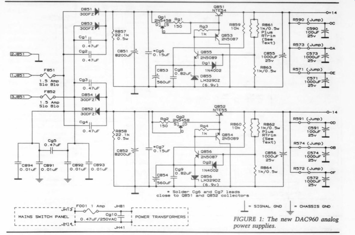
----- FIGURE 1: The new DAC960 analog power supplies.
The DAC chip makes far greater demands on the subsequent analog circuitry than those made by LP records or analog tapes, and this has very little to do with the wide dynamic range of digital audio. The output of a DAC contains ultra-high frequency sampling by products which are harmonically unrelated to the musical information. The digital byproducts require the subsequent circuitry be extremely linear at these frequencies, especially the I/V converter, which receives a signal from the DAC before any analog filtering has been applied. The 5534 is sorely lacking in this regard, and should not be used in any CD player or D/A converter claiming high-end performance.
Incidentally, the 5532 dual op amp, used by Philips and many other manufacturers to this day (including Nakamichi, in their $11,000 model 1000DARS DAT recorder), is essentially a dual version of the 5534, with minor differences. I'll give Philips credit for one thing-the use of single op amps in the DAC960 makes substitution of better devices much easier. The contortions we went through replacing 5532s with single devices in the older Magnavox CD players won't be necessary here.
Parts quality in the DAC960 is mediocre, with one exception. Philips used decent-quality Elna-Cerifine electrolytic capacitors for power supply bypassing, although they should have used much higher values. Unfortunately, they also used these electrolytics as audio coupling capacitors, without any film by passing. Even the best electrolytics should be avoided for coupling applications in high-performance equipment.
There's one instance where Philips used coupling capacitors redundantly.
The output buffer amplifier is coupled via an electrolytic to a signal routing relay. From there, the audio signal goes through yet another electrolytic capacitor before arriving at the fixed output jack.
Cheap carbon-film resistors are used throughout the analog and digital circuitry, and ceramic capacitors are routinely used for high-frequency power supply bypassing. But, there's good news, as well. The DAC960 contains no surface-mount chip-type components.
All resistors and capacitors are conventional parts with leads protruding through holes in printed circuit boards, making replacement very easy. Many readers know the difficulties of replacing chip components with conventional parts. Often, PC boards are so densely populated with tiny parts that replacement becomes nearly impossible.
The DAC960's analog regulators have poor rejection of line voltage variations. As the line voltage varies between 105 and 120V AC, the regulated DC outputs change by as much as 50mV. Dynamic regulation isn't particularly good either, but even if it were, Philips' insensible use of 'safety' resistors in series with the supply rails makes it a moot point. In older Philips designed products, these safety resistors varied in value from 33 ohm to as high as 100 ohm. They lowered the value to 3.3 ohm for the DAC960, low enough to make the “safety ” benefits highly question able, but still high enough to foul up the supply regulation. In order to keep power-supply output impedances as low as possible, series resistors should never be used in DC supply rails.
Ideally, the resistance between the regulators and the circuitry should be 02, or as close as humanly possible.
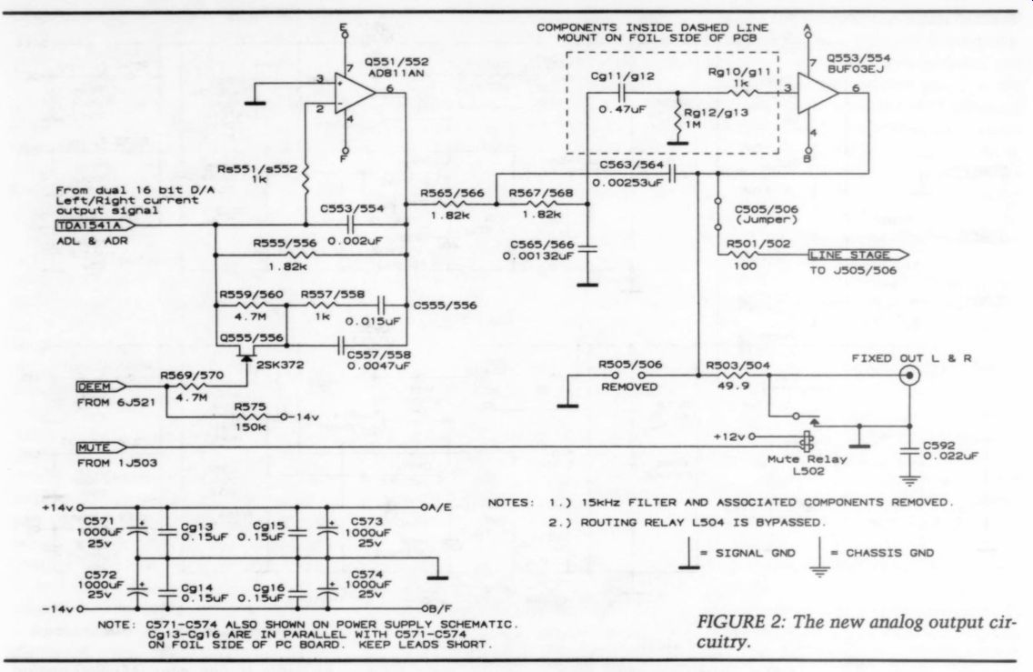
FIGURE 2: The new analog output circuitry. NOTE: C571-C574 ALSO SHOWN ON POWER SUPPLY SCHEMATIC. Cg13-Cg16 ARE IN PARALLEL WITH C571-C574 ON FOIL SIDE OF PC BOARD KEEP LEADS SHORT.
Philips used inexpensive, low cur rent, three-terminal regulators for all of the digital supplies, distributing the supply voltages to the PC boards with thin 24AWG wire. Local supply bypassing consists of very small value electrolytics, typically 47uF or less. Although their digital circuitry is very good, the high supply impedances don't provide these circuits with an optimum operating environment.
Supply Solutions
The analog supply regulators can't be fixed with simple parts substitutions- a completely new regulator design was necessary. The new 14V regulator circuits are shown in Fig. 1. You may ask why the rails have been set at +- 14V, rather than the customary +- 15V. The rail voltages were dictated by the toroidal transformer used by Philips, which has a 31V AC center-tapped secondary winding. Rectified, this produces only 22V raw DC. With the regulator volt ages set at +- 15V DC, regulation drops out when the line voltage falls below 110V AC. Lowering the rail voltages to + 14V solves the problem.
The original Philips regulators were also set to +-14V, even though the DAC960 service manual specifies +-15V. This doesn't affect dynamic headroom in any way. The rail voltages could be dropped to half these values and still be more than sufficient for the out put signal levels in the analog circuitry.
Remember, there aren't any signal levels higher than digital 0dB. With digital audio, there isn't any available head room above 0-dB--zero is the absolute maximum level.
There's a limit to how low these rails can be dropped, however. The - 14V rail also supplies the analog output currents for the TDA1541A DAC. If this voltage drops below -13V, the DAC won't operate. We believe that + 14V rails are the best compromise-they keep the regulators from dropping out at low line voltage, but are still high enough for pro per operation of the DAC.
For the positive regulator, the pass transistor Q851 operates in a complementary Darlington configuration with the Q853. R861 and R863 form the voltage divider and Q855 is the feedback transistor, or error amplifier. Zener diode D855 has been selected because of the low noise performance of the LM329DZ. Qg1 and Rg1 form a 4mA current source which biases Q851.
The regulator maintains constant DC output with varying line voltages, and its dynamic regulation characteristics are excellent. The negative regulator, of course, operates the same way, with all polarities reversed. Hampton picked the hefty NTE54/55 complementary pair for the pass transistors because of their high current gain, and high F; of 70MHz and 85MHz, respectively.
I know many of you will ask how this supply compares to the KG-5 sup ply I described in Ask TAA 4/90.
Quoting from that column: 'It would take a sophisticated discrete regulator to beat this IC-based design's performance. The new DAC960 analog supply is definitely a sophisticated discrete regulator.
We retain the original Elna-Audio grade 8200uF input-filter capacitors, since their performance characteristics are excellent. Panasonic-stacked film capacitors are placed across the rectifier diodes, to reduce noise, and ceramic bypass caps C891-894 are re placed with the Panasonic-stacked film types.
The Elna-Cerafine capacitors used for the output filtering and local supply bypassing are too low in value for low impedance bypassing. C855, 856 and C571-574 are replaced with 1000uF/ 25V Panasonic HF Q electrolytics. The HFQs are new to the Panasonic line, and feature even lower impedances for a given physical size than their predecessors, the trusty HFs. Panasonic ad vises us that the HFs are being discontinued and should not be used in new designs.
In the digital supplies, we've up graded the three terminal regulators to devices with 1.5A ratings. I've also up graded the two 220uF output filter caps to 560uF/10V HFQs. Since 6V negative regulators are sometimes difficult to find, we've changed this regulator to -5V. Philips' own application note on the TDA1541A shows -5V anyway, so I'm not sure why they chose -6V for the DAC960 (and most of their CD players containing this DAC).3 Low impedance bypassing is most important close to the digital circuitry.
Philips used capacitors ranging from 10uF to 47uF for digital supply bypassing. We've replaced all local bypass caps on the digital and input selector boards with 560uF HFQs. The cheap ceramic capacitors used for high frequency bypassing have been replaced with high-quality film capacitors. We also make an important power-supply regulation change in the phase-locked loop, replacing D359 zener diode with a low-noise precision zener. We use National's LM329DZ, which has a very low drift of 100PPM/degree C. This critical supply operates the loop's low New Analog Circuitry Figure 2 shows the new analog circuitry for the DAC960. The most critical circuit between the DAC and the output jacks is the I/V converter, for reasons I've mentioned above. Walt and I listened to a variety of high-performance IC amplifiers and finally settled on Analog Devices' AD811. This ultra high speed (2500V/ u-sec), wide-band HDTV video op amp is simply the best device I've heard in this application. It has the best dynamic contrasts, greatest inner detail and largest soundstage of any of the chips I tried (more on these comparisons in the listening comments, later).
The ADS811 is a transimpedance, or current feedback amplifier. Walt Jung's sidebar shows how these special de vices can be implemented in this application, laying to rest the rumor that they can't be used as integrating I/V converters. This op amp has a heavily biased, Class A output stage, so external current sources or pull-down resistors are unnecessary. The AD811 draws about 16mA of supply current at idle and should be used with a small heatsink.
The C553 and R555 (and their right
---------------------
High Performance Audio Stages Using Transimpedance Amplifiers
by Walt Jung
Transimpedance or current feedback amplifiers are still relatively new to audio applications, since they are primarily designed for video circuits.
While the AD846 (an early high-performance example) was successfully used in TAA, transimpedance amps may not be completely familiar de vices (The AD846 data sheet contains a detailed discussion of transimpedance amplifier theory). Interestingly, they possess several performance at tributes quite useful in audio circuits.
Among their virtues are very high slew rate and bandwidth, high output cur rent, and the ability to drive low impedance loads with excellent linearity. Because of these factors, more designers and audiophiles will use them.
Viewed from the exterior of an application, a circuit using a transimpedance amp can be deceiving. It can look just like one using a more conventional op amp. Both transimpedance amps and conventional (voltage input) op amps use a common symbol, and are often called op amps.
Nevertheless, their behavior can often be quite different.
The simplified gain expression for a non-inverting voltage-gain stage based on a transimpedance amp is similar to one using a conventional voltage input op amp. This gain “G” is expressed as:
G =1 + (Re/Rpy) (1)
Similarly, a current-to-voltage (I/V) converter using a transimpedance amp is like using a voltage input op amp counterpart, where the output voltage “V ” is:
V = -(In)Rg) (2)
What these two expressions don't show is that the feedback resistor R_F cannot be chosen freely with a transimpedance amplifier (as we know, it can be with the more familiar voltage input amplifier). This is because R; used in a transimpedance amplifier serves also as an element of the frequency compensation, along with an internal capacitor (C.). As a result, the gain of such a stage must be set via R,, when using a transimpedance amplifier, with R; a fixed value unique to a given amplifier type.
Usually, R; is optimized at the specific value which maximizes amplifier bandwidth, typically this is around 1 k-Ohm. While the designer has some limited freedom to vary R; by a small percentage, it will be at the expense of bandwidth variation (a higher R; value yields less band width; a lower value more). Some minimum value for R; must always be present in the feedback path for transimpedance amplifier stability.
This necessarily impacts applications beyond the case of the straight voltage-gain stage above, where the unique stability criteria for R; is al most transparent.
For example, while a conventional op-amp voltage follower can use a directly wired feedback connection from output to inverting input, a transimpedance voltage follower must use the specified value of R; for the given device. To use the example cited, a 1k) resistor from output to inverting input. This produces a transimpedance amp version of a voltage follower (more on this in the line stage example).
Because of the fundamental necessity for this frequency compensation resistor, it has been stated that trans impedance amps cannot be used in integrating I/V stages, such as the first analog stage of virtually all Philips family CD playback devices. This interface to the DAC is an integrating 1/V converter, forming the first section of a three-pole low-pass filter.
While it is certainly true that one can not simply drop a transimpedance amp into an integrator designed for a conventional op amp, it is not true that integrators cannot be made using transimpedance amps. Like the volt age follower, feedback can be effectively 100%, as long as a minimum R, value is present in the circuit for stability.
1) Bypass caps low-Z electrolytics in parallel with film caps.
2) Amplifier and stabilization resistor pre-wired to 8 pin header.
3) Use heat sink with ADB11AN, Aavid #5801 or equiv.
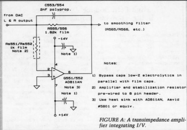
FIGURE A: A transimpedance amplifier integrating I/V.
Figure A is a case in point, and shows what is a basic first stage of the classic Philips 1/V conversion topology, an integrating I/V stage (de-emphasis circuitry not shown). When used with a conventional op amp, stabilization resistor Rg is not present, and this circuit forms the first filter pole of a three-pole Bessel rolloff as well as I/V conversion. The 1/V con version gain is set by the value of R555 and the DAC current output. The lo cation of the first pole is set by the
Continued on page 16
Continued from page 15 time constant R555-C553 (3.64us as shown), producing a corner frequency of 43.7kHz.
With a transimpedance amp used for the Q551 amplifier function, stability is provided by Rs551, using a value appropriate to the device and bandwidth desired. This technique was previously described in the OP160 datasheet, specifically as an integrator. In the circuit here, the main path is still from the DAC and R555/C553, while Rs551 carries the input error cur rent to the transimpedance amplifier Q551. In essence, Rs551 is performing the frequency compensation function, analogous in that sense to the classical connection of R;. Some performance figures with a high-grade transimpedance amplifier will serve to place the operation of this stage in perspective.
As connected here, and using an AD811 transimpedance amp, this circuit constitutes a voltage input op amp, as seen at the top of Rs551 (the I/V converter's summing junction).
The gain of a transimpedance amp is defined by its trans-resistance, Ry (that's where the name comes from).
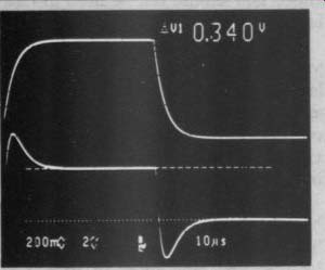
PHOTO A: Bench test of integrating I/V. V, (bottom) = error voltage x 100
v, (top) = Integrator output (10kHz square wave source).
The AD811 has a (loaded) Ry of 1.5M, so the net voltage gain from the summing point to the output is the ratio R;/Rs551, or 1.5E6/1E3 = 1500/1 (or, in dB, 63.5dB). For a 6V p-p out put signal from Q551, the input summing point error required to drive the Rs551/Q551 loop should be under 6mV p-p, a figure well below the recommended 25mV p-p compliance of the TDA1541 DAC family. This point in general can be a critical one, as most current output DACs have small compliance voltages for a specified linearity.
The open loop bandwidth of the ADS811 is determined by Ry and C- as:
For 1.5M and 5pF, this works out to be about 21kHz, very nicely accommodating the CD bandwidth.
A Dynamic I/V Test
To better illustrate how this trans impedance amplifier performs as an integrating I/V converter, some bench and CD playback tests we conducted as a demonstration, and are shown in Photos A-C.
Photo A shows the 1/V stage of Fig. A in a bench test, driven from a 0-4mA current source, which simulates the DAC being exercised with a full-scale step signal. This signal constitutes worst case conditions for the I/V in this CD application, both in amplitude and speed. Overload will show up as an abrupt change in the error voltage, which is V1, the bottom trace. The output of the I/V stage is V2, the top trace. For these measurements, a 100 x gain 8-pin instrumentation amplifier (AD620) was used to amplify the error at the summing point, “piggy backed ” on the AD811. Thus the “V1 ” voltages in the photos are divided by 100 to reflect actual input error. For reference, the AD620 has a small signal bandwidth of over 100kHz for this test, and a slew rate of 1.2V/pus.
Photo A shows a baseline error of 3.4mV p-p, rising somewhat higher with signal transitions. This is consistent with the calculated gain of the ADS811 as it is used here, and clearly there is no overload. The 3.4mV p-p error for a 4mA p-p signal current suggests that the dynamic impedance of this I/V terminating the DAC is 3.4E 3/4E-3 = 0.851%, or generally on the order of 12 or less. The dynamic volt age change of 5mV or less is useful in minimizing voltage compliance related errors, when used with any cur rent DAC.
Photo B shows the same I/V stage operating in an actual CD I/V converter, with exactly the same scope amplitude settings. The signal source is a 1002.27Hz square wave CD track, at 0dB amplitude.' Interestingly, the dynamic error voltage is exactly the same for the same output. Also, the large signal rate of change shown for this test is actually lower than the bench test of Photo A (therefore the bench test is more rigorous in this regard).
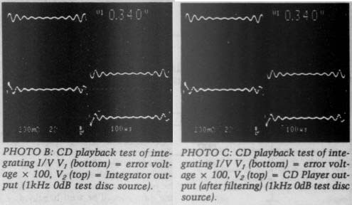
PHOTO B: CD playback test of integrating I/V V, (bottom) = error volt age
x 100, V, (top) = Integrator out put (1kHz 0dB test disc source). PHOTO C:
CD playback test of integrating I/V V, (bottom) = error volt age x 100,
V, (top) = CD Player out put (after filtering) (1kHz 0 dB test disc source).
Some small amplitude DAC steps are noted on these signals, and are shown more completely smoothed in waveform V2 of Photo C, the final out put of the CD player after traversing all three poles of filtering.
We also bench tested the AD846 with interesting results (not shown).
It revealed extremely small low frequency errors of only a few tens of mi crovolts, while the error on transitions is 2-3 times larger than the AD811.
With the AD846 this would generally be expected from the relatively higher R;, and the relatively lower band width and slew rate, vis-a-vis the AD811.
A Transimpedance Amp Line Stage
The above discussion has been a some what special case for audio applications, since I/V conversion is unique to digital audio uses. A circuit more broad in terms of application is a flat wideband line stage, such as the circuit of Fig. B.
This circuit is a wideband amplifier with an overall gain of five times, set ADB11AN 100 ohms FIGURE B: Composite JFET/transimpedance amp line stage.
Q651a and Q651b, with each optimized for their specific input/output functions. Q651a, a low-distortion AD744 JFET input op amp, provides low input current and a very high loading impedance, allowing direct coupling to the signal source. This will normally be a pot in the range of 10 50 k-Ohm, which is desirably very lightly loaded.
Since transimpedance amplifiers typically have input bias currents of about 1uA, they don't serve well used with relatively high source impedances (higher than 1 k-Ohm). Thus the JPET amplifier is optimum as an input interface, while Q651b (an AD811AN transimpedance amp) provides an ample load drive of more than 100mA. As you can see, Q651b is connected as a transimpedance amp unity gain follower, with the 1 k-Ohm R; serving as the frequency compensation resistor.
In this case, the overall composite connection of the AD744JN and the AD811AN work very well together, and the net distortion is quite low, on the order of - 100dB for several volts of output. As with the I/V circuit, heat sinking of the AD811AN is recommended for supplies above + 12V, and the power supplies of this composite line amp should be well bypassed.
REFERENCES:
1. Marchese, P., “High Performance Analog Circuitry for CD Players, ” TAA, 2/90, p- 8.
2. Rich, D., “A Brief Update on CD Players, ” The Audio Critic, #16, 1991, pp. 49-50.
3. “Analog Devices OP160 Data Sheet, ” 5/90, p. 19.
4. Whitney, D., Jung, W., “Applying a High-Performance Video Operational Amplifier, ”' Analog Dialogue, 26-1, 1992.
5. CBS CD-1 test disc, track 16.
6. Jung, W., Wurcer, S., 'A High Performance Audio Composite Line Driver Stage,' Analog Devices Seminar Notes, 1992.
------------------------
... channel counterparts) form the first pole of a three-pole Bessel filter. The other two poles are in the feedback loop of the output buffer amplifier. Hampton re-scaled the values of the filter components to yield common resistor values, since we're using a rather exotic resistor type in these critical locations and didn't want to have to buy three different values. These Caddock MK132s are among the finest resistors for audio applications available any where. I thank reader Paul Kelly for bringing them to our attention.
In less critical locations, we stick to the venerable Roederstein MK2s. All equalization and coupling capacitors are Panasonic P-series polypropylenes. The component values chosen by Philips for the de-emphasis circuit (R557/558, C555/556 and C557/558) are slightly changed, and the parts quality is up graded to the same level as the rest of the analog circuitry.
The output buffer amplifier is a PMI BUF03, a superb sounding Class A device designed as a unity-gain, open loop video buffer. The BUF03 competes head-to-head with Linear Technology's excellent LT-1010, but has three advantages. First, it is internally biased for Class A operation and doesn't require an external bias resistor (at +-14V it pulls nearly 18mA of supply current).
Second, it has very low DC offset even when operated open loop, and finally, it can be dropped right into a standard 8-pin opamp footprint.
The BUF03 has been around since 1979, but it's performance characteristics were years ahead of most audio IC op amps when it was introduced.* Today, few devices offering high-input impedance, low-input bias current and a high-current output stage can match its performance.
Although Philips incorporated a two resistor arrangement to null the 4V DC offset from the DAC, the resulting off set isn't sufficiently low, or stable over time, to allow DC coupling of the ana log circuits. A single-output coupling capacitor would solve the problem, but since it must be a high-quality film type for best sonic performance, its value will be physically restricted to around 10u uF. If low impedance loads are connected to the output of the DAC960, some bass rolloff will result.
There's an easy solution to this problem. Since the BUF03 has inherently low output offset, it makes sense to put a small value film-coupling capacitor at the input to the buffer amp, terminated in a very high 1M impedance. The 0.47 uF cap is a Panasonic P-series poly propylene. The output signal path has been “purified ” through the elimination of the unnecessary electrolytic coupling capacitors and resistors. A single 49.9 ohm series resistor for each channel sets the output impedance.
Unless you receive FM satellite transmission, you won't have any need for the 32kHz sampling rate and the 15kHz low-pass filter. I've simply re moved all of the components associated with the 15kHz filter. There's no sense having the filter pulling supply current if it's not going to be used. I also removed the routing relay and installed jumpers in its place.
High frequency supply bypassing is critical with such high-speed, wide band amplifiers, particularly the AD811.
The AD811 will oscillate due to stray supply-rail inductance if not properly by passed. As Fig. 2 shows, we've put a 0.15uF Panasonic V-series stacked-film cap across each of the four local HF Q bypass capacitors to eliminate the possibility of instability.
Digital Improvements
Since digital hardware appears to be what Philips does best, it's no surprise that the digital circuit topologies required the fewest changes. The most significant changes are in the digital input-selector circuits (Fig. 3). Philips used very high value feedback resistors around the 74HCU04 inverters. We've lowered the resistor to 1k, which in creases bandwidth, but it also lowers the input impedance. The input-termination resistors are increased to 100 ohm, and 100 ohm resistors are placed in series with the coupling capacitors. With the dynamic impedance of the active termination, this results in an input Z of 759.
The electrolytic coupling caps used by Philips are much higher in value than they need to be, and even with the small ceramic bypasses, the high frequency impedance is too high. The coupling caps are replaced with a 0.82uF Panasonic stacked-film capacitors.
Walt also made a change in the circuit supplying the de-emphasis volt age. The modified circuit is shown in Fig. 4. Originally, the de-emphasis volt age was + 3V, which actually saturates Q555/556. The new circuit feeds +0.7V to the gates of the FETs when a CD with pre-emphasis is played.
Project Complexities
This modification is an advanced project for experienced audio amateurs.
The complexities involved make this an unsuitable project for the beginner.
Many of the modifications require more than simple parts substitutions.
The analog power supplies and amplification circuitry involve retrofitting the PC board with circuitry sometimes incompatible with the existing PC lay out. Successful completion of the project requires the ability to understand a schematic diagram, implement the circuit changes within the confines of the existing PC layout, and verify that the circuits have been configured properly.
I'll give you quite a bit of guidance along the way, and I don't mean to sound intimidating. I simply wish to give you a realistic assessment of the project. I suggest reading the entire modification procedure thoroughly, perhaps more than once, before you decide whether or not to proceed.
You'll need some test equipment to verify proper operation. As a minimum, you should have a digital DC voltmeter (I really don't think a pointer-type “'analog ” meter is sufficiently accurate for trimming the analog power supply voltages), and an oscilloscope. A harmonic distortion analyzer isn't absolutely necessary, but it's the best tool for determining whether everything is really working properly. You'll also need a CD test disc with 1kHz tones.
I recommend the Denon Audio Technical CD #38C39-7147. Track 49 has a 1kHz tone at 0dB with pre-emphasis off.
Pierre Verany's two-disc Digital Test, #PV788031/32 is also suitable (item #CDPV/2 from Old Colony Sound Lab, $37.95 plus $2 S/H). Use track 24 on CD1. I don't recommend Woodford Music's Ultimate CD Test Disc, since the 1kHz tone on track 1 has inherently high harmonic distortion.
Some of you may have purchased DAC960s before Philips discontinued them nearly three years ago. If you don't own one and are interested in pursuing this project, I have good news.
Old Colony will have a limited number of brand new DAC960s at its disposal after the publication of the second part of this article (please do not inquire before that time). Purchased directly from Philips after they were discontinued, these will be for sale on a first come, first serve basis. Price information will be included in the second part of this article.
A DAC960 service manual is essential if you plan on performing these modifications. You must buy the ser vice manual from North American Philips-their address and phone number are in the parts list. They accept COD orders, which is probably the easiest method of purchase. If you'd rather send a check, you should call first to get the exact shipping and handling charges.
The DAC960 service manual is a marginal publication. As I guide you through these mods, you'll encounter many errors, including incorrect parts values and designators, parts which aren't on the schematics, incorrect volt ages, and so on. Fortunately, the parts' designators printed on the PC boards are usually correct. Although generally accurate PC board layouts are included, they only give views of the foil sides of the boards. This is a real pain, and a step backwards from my old CDB650 manual, which contained views of both sides of the PCBs. As bad as the manual is, I still consider it essential if you plan to modify your DAC960. I would have been quite lost without it and you shouldn't attempt these mods unless you have one.
The Mods Before beginning the modification instructions, I'd like to recommend a couple of tools which will make your life much easier. First, nothing beats a good desoldering tool for removing old components, especially integrated circuits. Short of spending hundreds of dollars on a vacuum-driven desoldering station, the best tool I've found is Radio Shack's #64-2060 at a whopping $8.49.
The Radio Shack desoldering tool makes IC and other component removal a snap, and works so quickly that you avoid damaging the circuit board traces.
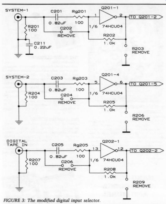
FIGURE 3: The modified digital input selector.
I should mention that I abhor solder wick and never use it.
The photo in Radio Shack's catalog doesn't show the best method for using the desoldering tool. Here's mine. Hold the tool by gripping the red rubber bulb between your thumb and forefinger.
While holding the tool away from the PC board, squeeze the ball. Then, keeping the ball squeezed, move the tip over to the PCB, heat the connection and release the ball. Move the tool away from the board again and squeeze the ball two or three time to clear out the excess solder, preferably over a waste basket. You should periodically “tin ” the tip of a desoldering tool, as you would any normal soldering iron.
I also recommend a Phillips retainer type screwdriver for removing the screws that hold the PC boards in place. These screwdrivers have a retaining clip on the end which make it easier to get the screws in and out of tight places. Finally, you might consider using lead-free silver solder for the analog circuit changes (I'm not convinced that there would be any sonic benefit to using it for the digital mods, but don't consider this statement gospel!). I use Radio Shack #64-025 which is 96% tin and 4% silver. One word of caution--lead-free solder joints aren't shiny like joints made with standard lead/tin solder. They actually look like a cold solder joint, but they're not. You really need to be extra careful not to disturb the joint before it cools, since lead-free solder doesn't give you any visual indication of the quality of the joint.
[20]
lists, I use the following abbreviations to identify various Panasonic capacitors:
PP = P-series polypropylene
SF = V-series stacked film
HF Q = HF Q series aluminum electrolytic
XY-series interference suppression Be sure to observe polarity when in stalling the HF Q electrolytics.
Refer to the supply and mute circuit schematic on pages 24 and 25 of the DAC960 service manual. Remove the metal shield covering the digital-supply power transformers. Unplug the two transformer connectors, J801 and J802, from the board along with the four white DC supply connectors J803 through J806 on the front of the board.
Philips has harnessed the DC supply cables in such a way that it's difficult to reinstall the connectors in the wrong locations, but you may wish to label them, just to be safe. Remove the PP16 board.
Replace Q801 and Q802 each with an LM7805/LM340T5 positive 5V, 1.5A regulator. The pinouts are the same as the old regulators.
Replace Q803 with an LM7905 negative 5V, 1.5A regulator. The pinout is the same as the old regulator.
Replace C806 with a 560uF/10V HEFQ.
Replace C807 with a 560uF/10V HFQ.
Connect a 0.47uF/100V SF across each rectifier diode in the digital sup plies. There are a total of 12 in parallel with D801 through D812.
These can hang from the diodes be tween the diodes and the PC board.
Connect a 0.47uF/100V SF across each transformer secondary connector on the board (three total). These should be soldered to the foil side of the board, across the blue/green leads at J801, the blue/green leads at J802 and the yellow/orange leads at J802.
Replace R810 with a 220K, ¼ W resistor. This increases the power-on delay to approximately eight seconds.
Connect a 6802, 3W resistor between the outputs of Q802 and Q803. This biases the regulators more heavily for improved dynamic regulation.
Connect a 1N4002 diode between the input and output of Q803, on the foil side of the board. Solder the anode to the input and the cathode (stripe) to the output. This reverse biases the diode during normal operation, but insures that the regulator's IS = output will never be higher than the input during power down (which may happen with the large amount of bypass capacitance we're adding across the output). If this diode is in stalled backwards, you'll blow fuses when you turn the DAC960 on, at the very least.
Connect a 1N4002 diode between the input and output of Q801, on the foil side. The cathode should be connected to the input, and the anode to the output. Do the same for Q802.
Again, carefully observe polarity.
Reinstall the PP16 board and recon nect only the power transformers.
Power up the DAC960 and measure the supply voltages, as indicated on the schematic. Remember that the old
- 6V supply is now --5V. Once you've verified correct supply voltages, turn the power off and allow 5 minutes for the supply voltages to drain. Reconnect the remaining cables. Connect the DAC960 to a CD transport and verify proper operation, preferably with a CD test disc and an oscilloscope.
TABLE 1 PROCEDURE 1: PP16
DIGITAL POWER SUPPLY
Regulators ( 2) LM7805/LM340T -5, 5V positive regulators (Q801, 802). Digi-Key #LM340T -5 ( 1) LM7905, 5V negative regulator (Q803).
Digi-Key #LM7905CT Capacitors ( 2) 560 uF/10V HF Q (C806, 807).
Digi-Key #P5640 (15) 0.47 uF/100V SF. Digi-Key Pa733 Resistors ( 1) 220k/vaW (R810).
( 1) 6800/3W. Digi-Key #P680W -3 Diodes ( 3) 1N4002. Digi-Key #1N4002
Procedure 2: Digital Input Selector Remove the small metal shield covering the PJ16 digital-input selector board. Put the shield and the two screws in a safe place-you won't re install them until the project is finished. Unplug the PJ16's cable harness from the PD16 demodulator board and remove the PJ16 from the rear panel.
It's held in place with one screw in the middle of the input RCA jack assembly.
You'll notice that the service manual indicates 74HC04 hex inverters in this circuit. The board has 74HCUO4s.
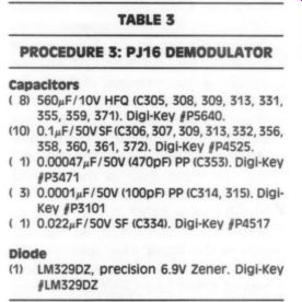
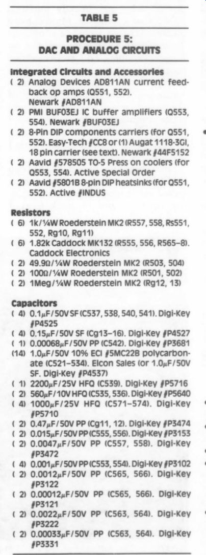
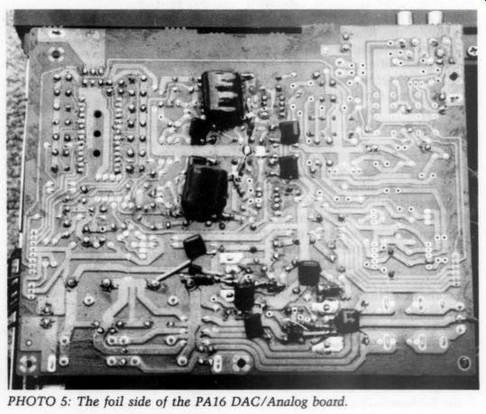
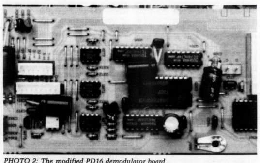

FIGURE 4: The modified de-emphasis activation circuit.
Refer to the Input Selector Circuit schematic on page 13 of the service manual, and to Fig. 3, the modified in put circuits.
Remove R203, R206 and R209. These are left open.
Remove C202, C204 and C206.
These are left open.
Replace C201, C203 and C205 with a series RC network consisting of a 10 0-Ohm/ 1/4W resistor and a 0.82uF SF capacitor. Install them so the resistors are toward the 74HCU04 ICs and the capacitors are toward the input jacks. Each cap can lie sideways on the PC board, with the lead closest to the board bent at a right angle, and pushed through the hole in the board.
The resistor should stand up straight, with one lead through the PC board and the other soldered to the capacitor. Be sure the leads are short where the capacitor and resistor are joined, so they won't hit the rear panel when the board is reinstalled. The removal of C202, C204 and C206 leaves extra holes in the PC board to facilitate spacing.
Replace R201, R204 & R207 each with 10 0-Ohm/ 0.5 W. These resistors aren't shown in the schematic, but are correctly labeled on the board.
Replace R202, R205 and R208 each with 1k/ 0.5 W.
Replace C214 with a 0.1uF/50V SF.
Replace C213 with a 560uF/10V HFQ.
C213 is incorrectly marked C212 in the schematic. It's correctly labeled C213 on the PCB. The capacitor should lay flat on top of Q203.
Put short lengths of sleeving over the exposed leads.
Remove electrolytic C207 and its ceramic bypass C208. The physical locations of the electrolytic and the film bypass are going to be reversed, to facilitate installation. Electrically, there's no difference. Replace C207 with a 0.1uF SF. Replace C208 with a 560uF/10V HFQ, laying the capacitor on top of Q201, and using short lengths of sleeving over the expose leads. Use the board marking for C207 to indicate correct polarity for the new C208.
Replace C210 with 0.1 uF/50V SF.
Replace C212 with 0.1 uF/50V SF.
Photo 1 shows the modified PJ16 board. Reinstall the board on the rear panel. The wiring harness will fit comfortably between the RCA jacks and the 560uF cap at C208. There's a small step on the RCA assembly that the wires will rest against. With everything in place the RCA assembly will seat properly in the four holes, and the pair of 560uF HF Q caps will fit snugly be tween the ICs and the rear panel. It's virtually a zero-tolerance fit, but it works. The small metal shield won't be reinstalled until the entire project is completed.
TABLE 2
PROCEDURE 2:
PJ16 DIGITAL INPUT SELECTOR
Capacitors (2) 560.F/10VHF Q (C207, 213). Digi-Key #P5640 (3) 0.82 ,F/50V SF (C201, 203, 205). Digi-Key
P4a536 (4) 0.14F/50V SF (C208, 210, 212, 214). Digi-Key
P4525 Resistors (6) 1000/vW Roederstein MK2 (R201, 204, 207, Rg201, 203, 205) (3) 1.0k/vaW Roederstein MK2 (R202, 205, 208) T
Procedure 3: Demodulator Board Refer to the PD16 Demodulator and Sampling Frequency Display schematic on pages 8, 9 and 10 in the DAC960 service manual. Unplug the wiring har nesses J301 and J303. The PD16 board is fastened to a long black bracket with three screws. Remove the bracket from the chassis, and the board from the bracket. The two small wiring harnesses J304 and J305 are soldered. There should be enough slack to allow you to work on the PD16 board. You may have to carefully cut a few cable ties to give yourself some slack in the wiring.
Carefully unsolder the metal shield on the board. You'll have to unsolder the two metal tabs on the foil side.
If you heat the tabs quickly, you can pull off the cover before it gets warm.
Clean the remaining solder from the slots in the PCB with your Radio Shack desoldering tool. Be sure you don't move trimpot R351 during these modifications. If you do, you'll have to reset it following the procedure given in the service manual.
Replace C353 with 0.00047uF/50V (470pF) P-P.
Replace C356, C358 and C361 each with 0.1 uF/50V SF.
C361 isn't on the schematic, but it's labeled on the board.
Replace C355 with 560uF/10V HFQ.
Bend the tab on the shield slightly so it clears the new C355 and replace the shield. It must be re-soldered in place.
Replace C331 with 560uF/10V HFQ.
Replace C332 with 0.1uF/50V SF.
Replace C305 with 560uF/10V HFQ.
Replace C306 with 0.1uF/50V SF.
Replace C308 with 560uF/10V HFQ.
Position this capacitor against the PCB, facing the top of the board. Add short lengths of sleeving to cover the exposed leads.
Replace C307 with 0.1uF/50V SF.
Replace C313 with 560uF/10V HF Q in parallel with 0.1 uF/50v SF. This capacitor is mislabeled C358 in the schematic, but the board designator is correct. The negative side of the HF Q will lie flat against the board between Q305 and the 7220P/B filter, Q302. The leads of the 560uF cap should be bent at a right angle, to ward the C313 location. Add short lengths of sleeving on both leads, and bend them at a right angle again, so they will go through the PCB holes.
Be sure the leads are insulated from the jumper underneath. Important:
The positive lead of the 560uF cap goes in the hole which connects to Pin 1 of Q305. The negative lead goes toward pin 7 of Q304, which is ground. Now insert the 0.1uF SF through the same holes. The PCB holes are large enough to accommodate the leads of both capacitors.
Position the 0.1uF SF cap as close to the board as possible.
Replace C371 with 560uF/10V HFQ.
This capacitor isn't in the schematic.
Lay the new cap on its side, with the top facing the SAA7220P/B digital filter. Put sleeving over the longest exposed lead.
Replace C372 with 0.1uF/50V SF.
This cap isn't in the schematic.
Replace C359 with 560uF/10V HFQ.
Position the cap on top of the jumper next to J303, facing the top of the board. You may wish to slip a small cable tie between the jumper and the board to hold the cap in place. Put sleeving over the exposed leads-3/8 ” on the negative lead and 3/4 “ on the positive. The bottom of this capacitor must be at least 7/8 “ from the bottom edge of the board to prevent interference when the board is re installed.
Replace C360 with 0.1uF/50V SF.
Replace C309 with 560uF/10V HF Q in parallel with 0.1uF/50V SF. The 560uF cap should lie on its side against the board, with the top facing C359. The PCB holes are large enough to accommodate the leads from both capacitors. The 0.1 uF cap should be as close to the board as possible, but be sure the leads clear the neighboring jumper. The positive lead of the HF Q is toward the bottom of the board.
Replace C334 with 0.022uF/50V SF.
This capacitor goes between the PC board ground and the chassis, al though it isn't in the schematic.
Replace C314 with 0.0001 uF/50V (100pF) PP. This capacitor isn't in the schematic or the PC layout, but it's clearly labeled on the board.
Replace C315 with a pair of 0.0001 uF/50V (100pF) PP capacitors connected in series. This gives an equivalent value of 50pF; the original is 47pF. This cap isn't in the schematic or the PC layout, but it's clearly labeled on the board.
Replace zener diode D369 with LM329DZ. The LM329DZ has three leads, but only two are used. Figure 5 shows the pinout. As you face the flat side of the diode, cut off the left lead. The middle lead is the cathode and the right lead is the anode.
Remove C333 and don't replace.
Refer to Fig. 4 and the PD16 schematic for the de-emphasis changes.
Remove R380 and don't replace.
Remove R381 and replace with a jumper.
R379 isn't changed. Although Philips' schematic shows 47 0-Ohm, they actually used 2.2k, as I've indicated in Fig. 4.
Philips also shows an NPN transistor for Q375, and mislabels it 2SA733. It's really a 2SA1048, which is a P-N-P de vice. I mention this for clarification.
The modified PD16 board is shown in Photo 2. Carefully check the installation of all components, especially the orientation of the electrolytic capacitors. Screw the metal bracket back onto
the board and reinstall the board. The bottom of the board will rest in the six small channels in the aluminum chassis. Be very careful that you don't pinch any wires when the board is reinserted, especially those near the bottom, front portion of the board. Also be sure zener D359 and SF cap C360 don't hit the PA26 line stage board.
Reconnect everything and test the DAC960 for proper operation, preferably with a test CD and “scope. You can verify proper operation of the de-emphasis circuit by selecting a track on your test disc with pre-emphasis ( “emphasis on ”). The DEEM line should rise to 0.7V DC. Now select a track with out pre-emphasis. The DEEM line should drop to around -14V DC.
TABLE 3 PROCEDURE 3: PJ16 DEMODULATOR Capacitors ( 8) 560 uF/10V HF Q (C305, 308, 309, 313, 331, 355, 359, 371). Digi-Key #P5640.
(10) 0.1 uF/50VSF (C306, 307, 309, 313, 332, 356, 358, 360, 361, 372). Digi-Key #P4525.
( 1) 0.00047uF/50V (470pF) PP (C353). Digi-Key P3471 ( 3) 0.0001.F/50V (100pF) PP (C314, 315). Digi Key #P3101 ( 1) 0.022 ,F/50V SF (C334). Digi-Key P4517 Diode (1) LM329DZ, precision 6.9V Zener. Digi-Key fLM329D2 Procedure 4: Analog Power Supplies We'll start with a simple enhancement for the DAC960's AC power-line filter.
Refer to the supply and mute circuit schematic on pages 24 and 25 of the service manual, the PC board layouts on page 27, and Fig. 1.
Solder 0.47uF/250V AC IS capacitor across the AC power line be tween the PH16 mains-switch panel board in the left rear corner of the chassis, and the power transformers.
This cap is Cgl0 in Fig. 1. The most effective place to solder this cap is between terminal JH81 and JH41 on the small PC16 transformer-inter connect board. Use sleeving on any exposed leads.
Now, refer to the Supply-DAC-Out put circuits on pages 20 and 21 of the DAC960 manual and the new analog power supply circuit shown in Fig. 4.
Remove the balanced output connectors from the rear panel. Unwrap the wire-wrapped ground connections at … JG97 and JG98. Cut all cable ties holding the shielded cables in place, and unplug the cables at J703 and J704 on the PA26 line stage board.
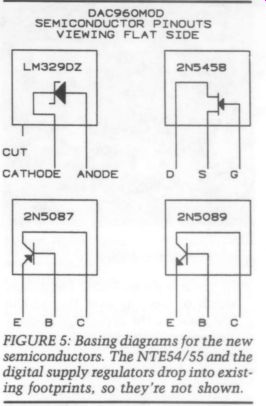
FIGURE 5: Basing diagrams for the new semiconductors. The NTE54/55 and the digital supply regulators drop into existing footprints, so they're not shown.
These connectors and cables won't be reinstalled as part of POOGE-5, but you may want to save them.
Remove the rear panel, held in place with eight screws, including two into the optical connector, and one in the center of the audio output-jack assembly. It isn't necessary to re move the digital input board-just be sure to unplug it from the DD16 de modulator board. The shield for the digital input board hasn't been rein stalled at this point, and won't be until the project is completed.
Unplug the power transformer connector at J851 (mislabeled J523 in the service manual), the DC supply connector next to it at J503, and the harness going to J301 on the demodulator board. Note that J521 and J523 on the PA16 board are soldered in place and won't unplug.
The 5V supply connector J523 runs all the way over to the digital power supply board. If you wish to completely remove the PA16 board, which I recommend, you must carefully cut all of the small cable ties holding the 5V supply harness in place, unplug the J803 connector on the digital supply board, and remove the cable. It may be a little tricky untangling this cable from those it's tied to, so be patient.
Remove the five screws holding the PA16 board in place, and remove the board.
Remove the following components, which won't be replaced:
Q581, Q582 (15kHz low-pass active filter modules) L504 (Signal routing relay) C511, 512 C611, 612 C581, 582 C503-508 C895, 896 R581-584 R505-508 This clears the PC board of a lot of un necessary clutter.
Remove the six 3.3 ohm “safety ” resistors and replace them with jumpers:
R571-574 R590, 591 (The local bypass caps for the 15kHz filter are still across the supply rails-they can't hurt, and they're free!) Next, we'll replace several ceramic capacitors between PC board ground and chassis ground. Some aren't in the service manual, but the board is clearly labeled.
Replace C592 with 0.022uF/50V SF.
Replace CG85 with 0.0022uF/50V PP.
Replace CG86 with 0.0022uF/50V PP.
Replace CG81 with 0.022uF/50V SF.
Replace CG82 with 0.0001uF/50V (100pF) PP.
Replace CG83 with 0.0022uF/50V PP.
Replace CG84 with 0.022uF/50V SF.
The analog power supply changes are next. Refer to the schematic on page 20 of the manual, and to Fig. 1.
Replace C891-894 each with 0.01uF/ 50V SF.
Replace R857 and R858 each with 22.1k/0.5W Roederstein MK3 resistors.
Install four 0.47uF/100V SF capacitors, Cg1 through Cg4, in parallel with D851-854. These hang below the rectifier diodes, as they do in the digital supplies.
Install Cg5, a 0.47uF/100V SF on the foil side of the board, between fuse holders F851 and F852. Be sure it's installed on the rectifier side of the fuse holders, for maximum effectiveness.
Replace Q851 with NTE54. You must unsolder the heatsinks from the board, as well as the transistor leads. Use a small amount of white thermal compound. The NTE54 is pin-compatible with the old transistor.
Replace Q852 with an NTESS.
Follow the same procedure for Q851.
The pin-out is the same as the old transistor.
Remove the rest of the existing power supply components:
Q853-856 R853-856, 859, 860, 861-864 C853-856 (mislabeled X856 in the service manual) D855, 856 Some of the new power supply components drop right into existing locations. We'll start with these:
Install 560uF/10V HF Q capacitors at C853 and C854.
Install 1000 uF/10V HFQs at C855 and C856.
Install 1k/ 0.5 W Roederstein MK3 resistors at R863 and R864.
Install 1k/ 0.5 W Roederstein MK3 resistors at R861 and R862. These resistors should sit about 3/4 ” above the PC board.
Install 10k/ 0.5 W Roederstein MK2 resistors at R859 and R860.
The rest of the components don't drop into existing footprints, except for the zener diodes. I'll guide you through an installation procedure which will make the new circuit topology fit the existing PC board layout:
Install a 2N5089 transistor at Q855.
The flat side faces the rear of the PC board. Carefully note the pinout of the 2N5089, as shown in Fig. 5. Facing the flat side, the original Q855 PHOTO 3: The modified PA16 analog power supply regulators.
PC board holes are E-C-B. Put a short length of sleeving over the middle lead (base) of the 2N5089, and cross the base and collector leads to fit the existing footprint.
Install a 2N5087 transistor at Q856.
Follow the same installation guide I just gave for Q855, noting its pinout in Fig. 5.
Put a short length of sleeving over the center lead (base) of a 2N5089.
Insert the emitter and base leads, along with 1k/ 0.5 W resistor Rg4, into the outer PC holes for old Q854.
Don't use the middle hole. Then, insert the collector lead in the hole for the cathode of D856, but don't solder it yet. The flat side of this transistor faces the rear of the board.
Install an LM329DZ zener diode at D856, cutting the unused lead just as you did for D359 on the PD16 board. Solder only the cathode in the same hole with the collector of Q854, which is PC board ground.
Install an insulated jumper between the anode of D856 and the minus lead of C854. One end of the jumper shares the PC hole with the anode, and the other end goes in the forward most hole left vacant by the removal of R856.
Put a short length of sleeving over the center lead (base) of a 2N5087.
Insert the emitter and base leads, along with 1k/ 0.5 W resistor Rg3, into the outer PC holes for old Q853.
Don't use the middle hole. Angle the collector lead toward the D855 cathode location, but don't connect it to anything yet. The flat side of this transistor faces away from Q851's copper heatsink.
Install an LM329DZ zener diode at D855, cutting the unused lead.
Solder only the anode. Then, solder the collector lead from Q853 to the middle of the anode lead of the diode.
Install an insulated jumper between the cathode of D855 and the plus lead of C853. One end of the jumper shares the PC hole with the cathode, and the other goes in the forward most hole left vacant by R855.
Install Cg6 and Cg7, 0.15uF SF caps, across C851 and C852, on the foil side of the board. One lead of each cap should be as close to the collectors of Q851 and Q852 as possible.
Install Dg1 and Dg2, 1N4002 diodes between the base and emitter of Q855 and Q856, respectively. Note that the diode polarity is reversed across each base/emitter junction.
Solder them to the foil side of the board.
Install Cg8 and Cg9, 0.82uF SF caps, across D855 and D856, on the foil side of the board.
-----------
Respighi: The Pines of Rome, Dutoit, Montreal Symphony, London 410415-2.
Schoenberg: Five Pieces for Orchestra, Dorati, London Symphony, Mercury 432 006-2.
Mussorgsky/Ravel: Pictures at an Exhibition, Reiner, Chicago Symphony, RCA RCD1-5407.
Stravinsky: The Rite of Spring, Maazel, Cleveland Orch., Telarc CD 80054.
Verdi: Aida, Tebaldi, Bergonzi, Simionato, Karajan, Vienna Phil., London 414-087-2.
Wagner: Gotterdammerung, Nilsson, Windgassen, Solti, Vienna Phil., Lon don 414 115-2 (especially “Siegfried's Funeral Music,' CD4, Tr. 7, 4:07).
Wagner: Siegfried, Nilsson, Windgassen, Solti, Vienna Philharmonic, Lon don 414 110-2, (especially the 'Forging Scene ” in Act I, CD2, Tr. 1-5).
Dvorak: Symphony No. 9 (' New World ”'), Horenstein, London Symphony, Chesky CD31.
Respighi: The Birds, Dorati, London Symphony, Mercury 432 007-2.
Bruckner: Symphony No. 8, Jochum, Berlin Philharmonic, DG 429 079-2 (especially Mvt. 4).
--------------------
See Fig. 5 for the pinout of the 2N5458 current source J-FETs, Qgl and Qg2. Each current source can be made by bending the middle lead straight up and soldering it to one lead of the 1509 resistor (Rgl and Rg2). The other end of the resistor is soldered to the gate. Put a small piece of sleeving over the drain leads, and solder each current source as sembly to the foil side of the board.
Carefully note the orientations of the current sources. Slip a piece of 34 ” flexible tubing over each assembly, to prevent contact with the board.
Carefully re-check the entire power
TABLE 4
PROCEDURE 4:
PJ16
ANALOG POWER SUPPLY
Semiconductors (1) NTES54 transistor (Q851). Mouser #526-NTE54 (1) NTESS transistor (Q852). Mouser #526-NTES5 (2) 2N5458 N-channel J-FETs (Qg1 and Qg2).
Active # INDUS (2) 2N5087 transistors (Q853, 856).
Digi-Key #2N5087 (2) 2N5089 transistors (Q854, 855).
Digi-Key #2N5089 (2) LM329D2Z precision 6.9V Zener diodes (D855, 856). Digi-Key #LM329D2 (2) 1N4002 diodes (Dg1, 2). Digi-Key #1N4002 Resistors (2) 22.1k/ 0.5 W Roederstein MK3 (R857, 858)
@ 1k/ 0.5 W Roederstein MK3 (R861-864) (2) 8.25k/%4W Roederstein MK3 (R861 gy and R862 7pm) (2) 10k/vaW Roederstein MK2 (R859, 860) (2) 1k/vW Roederstein MK2 (Rg3, 4) (2) 1500/ 0.5 W Roederstein MK2 (Rg1, 2) Capacitors (2) 1000 uF/25V HF Q (C855, 856). Digi-Key
#P5710 (2) 560uF/10VHF Q (C853, 854). Digi-Key #P5640 (1) 0.47,/250V AC IS (Cg10). Digi-Key #P4614 (5) 0.47 uF/100V SF (Cg1-5). Digi-Key #P4733 (4) 0.01.F/50V SF (C891-894). Digi-Key #P4513 (2) 0.154F/50V SF (Cg6, 7). Digi-Key #P4527 (2) 0.82 uF/50V SF (Cg8, 9). Digi-Key #P4536 Ground-to-Ground Bypass Capacitors (3) 0.022 uF/50V SF (C592, CG81, 84). Digi-Key
PAas517 (3) 0.0022uF/50V PP (CG83, 85, 86). Digi-Key
P3222 (1) 0.0001uF/50V (100pF) PP (CG82). Digi-Key P3101
Continued from page 24
supply circuit. Verify the electrical connections for each component to make sure that your circuits are electrically identical to the schematic in Fig. 1. We will now trim R861 and R862 to obtain the correct supply voltages.
Temporarily tack solder a pair of 8.25k/ 0.5 W resistors across the 1k/0.5W resistors R861 and R862.
Don't shorten the leads just yet, but make sure the leads don't touch any other components. You may wish to put sleeving over the long leads.
When you are absolutely certain the power supply circuits are correct, re install the PA16 board and connect the power transformer at J851. You don't need to connect any other cable assemblies at this time.
Turn on the DAC960 and check the rail voltages. The easiest places to measure the DC voltages is on the jumpers installed at R591 and R573.
The supply rails should be +14V DC, but tolerances of the zeners D855 and D856 may cause variations. The voltages should be no lower than +-13.9V and no higher than +14.2V. I got lucky-the 8.25k resistors in parallel with the 1ks gave me +- 14.1V. If the zeners are exactly 6.9V the trimmed equivalent resistance should be 8879.
If your supply voltages are too high, lower the trim resistor values. If they're too low, the values should be raised.
Once you've determined the correct trim resistor values, solder them in place permanently, with leads as short as possible. Re-check the voltages to make sure they're within the specified tolerances. You've just completed the most difficult and tedious part of the DAC960 modifications. Photo 3 shows the new PA16 supply regulators.
Procedure 5: DAC and Analog Circuits Replace C521-534 with 1.0uF/50V ECI polycarbonate capacitors. Stand the caps vertically with the shortest leads closest to the TDA1514A DAC. Put sleeving over the long leads of the seven caps near the edge of the board. De pending on price and availability, you can substitute 1.0uF/50V Panasonic SF caps for the ECIs, with a very slight performance degradation. Walt and Hampton find the high end to be a bit smoother with the ECIs. Elcon Sales assures me that they'll continue to supply the ECI capacitors.
Replace C539 with 2200uF/25V HFQ.
Replace C535 and C536 each with 560uF/10V HFQ.
Replace C537, 538, 540 and 541 each with 0.1 uF/50V SF.
Replace C542 with 0.00068 (680pF)/ 50V P-P.
Refer to pages 20 and 21 in the service manual, and Fig. 2, the new analog circuitry.
The PC board contains holes for compensation capacitors between pins 5 and 8 of Q551 and Q552, as well as pins 2 and 3 of Q553 and Q554. None of the DAC960s we've seen actually had capacitors in these locations. If yours does, remove them and don't replace them.
The AD811AN op amps must be in stalled with 1k/ %4W resistors Rs551 and Rs552 in series with pin 2, as shown in Fig. 2. The easiest way to do this is to mount the AD811 on a component carrier or header, soldering the resistor between op amp pin 2 and pin 2 of the carrier. Eight pin DIP carriers are hard to find. You could buy an 18 pin carrier, pull out the middle pins, and slice it in half, making a pair of 8-pin carriers. Bend pin 2 of the op amp straight up, at the point where the pin becomes thinner. Solder the op amp to the top of the carrier, then solder the resistor between carrier pin 2 and op amp pin 2. Don't allow any solder bridges between the pins. Be sure the resis tor doesn't stick up too far-it must clear the heatsink. Finally, slip 8-pin DIP heatsinks over the op amps.
Make sure the heatsinks clear the 1k resistors.
Replace Q551 and Q552 with the AD811 assemblies you just finished.
Make sure the notches in the new ICs match those on the board.
Replace C571-574 each with a 1000uF/25V HFQ.
On the foil side of the board, solder four 0.15uF/50V SF capacitors in parallel with C571-573 and C574.
These are Cgl3-16 in Fig. 2. Keep the leads short.
Replace R557 and R558 each with 1k/ 0.5 W Roederstein MK2 resistors.
Replace R555, R556, R565 and R566 each with 1.82k Caddock MK132 resistors. The Caddock resistors actually look like small capacitors.
Replace C553 and C554 each with two 0.001uF/50V PP capacitors in parallel, making a pair of 0.002uF caps. Both caps will fit in the PC holes. Keep the leads short.
Replace C555 and C556 each with 0.015/50V PP.
Replace C557 and C558 each with 0.0047uF/50V PP.
Remove the remainder of the old components associated with the out put buffer/filter circuit:
Q553 and Q554 (mislabeled Q534 in the service manual) L551 and L552 (not shown in the service manual) C563-566 R567 and R568 Next, we'll construct the new output buffer/filter circuit as shown in Fig. 2.
It's not compatible with the existing PC layout, mainly because of the added input coupling circuit shown inside the dashed line. But, since L551 and L552 aren't replaced, we have some layout flexibility. I'll explain how to implement the new circuits without cutting any PC traces.
Select a pair of BUF03E IC buffer amplifiers. They will be installed at Q553 and Q554. Group the leads in two rows of four each, so they will fit into the 8-pin DIP footprints on the PC board. The metal tab on the BUFO3EJ identifies pin 8. When you are absolutely certain you've identified the leads according to their pin numbers, cut pin 2 on both ICs close to the case. Mount the Aavid TO-5 press-on coolers on the BUF03E]s, and install the assemblies at Q553 and Q554, paying careful attention to the pinout of the ICs. The metal tabs on the BUFO3EJJs are on the notched end of the PC board pattern.
Install two 1.82k Caddock MK132 resistors each at L551 and L552.
These are really R567 and R568 in Fig. 2, but they're not installed in the old R567 and R568 locations.
TABLE 5 PROCEDURE 5:
DAC AND ANALOG CIRCUITS
integrated Circuits and Accessories ( 20 Analog Devices AD811AN current feed back op amps (Q551, 552).
Newark fAD811AN ( 2) PMI BUFO3EJ IC buffer amplifiers (Q553, 554). Newark #§BUFO3EJ ( 2) 8-Pin DIP components carriers (for Q551, 552). Easy-Tech §CC8 or (1) Augat 1118-3Gl, 18 pin carrier (see text). Newark §44F5152 ( 2) Aavid #578505 TO-5 Press on coolers (for Q553, 554). Active Special Order ( 2) Aavid #58018 8-pin DIP heatsinks (for Q551, 552). Active #INDUS Resistors ( 6) 1k/vaW Roederstein MK2 (R557, 558, Rs551, 552, Rg10, Rg11) ( 6) 1.82k Caddock MK132 (R555, 556, R565-8).
Caddock Electronics ( 2) 49.90/v 0.5 W Roederstein MK2 (R503, 504) ( 2) 1000/v4W Roederstein MK2 (R501, 502) ( 2) 1Meg/vW Roederstein MK2 (Rg12, 13) Capacitors ( 4) 0.14F/50VSF(C537,538, 540, 541). Digi-Key
§P4525 ( 4) 0.154F/50V SF (Cg13-16). Digi-Key P4527 ( 1) 0.00068uF/50V PP (C542). Digi-Key #P3681 (14) 1.0 uF/50V 10% ECI §5MC228B polycarbonate (C521-534). Eicon Sales (or 1.0 uF/50v SF. Digi-Key #P4537) 2200.F/25V HF Q (C539). Digi-Key #P5716 560 uF/10V HF Q (C535, 536). Digi-Key #P5640 1000 uF/25V HF Q (C571-574). Digi-Key
#P5710
0.47 uF/50V PP (Cg11, 12). Digi-Key §P3474
0.015 uF/50V PP(C555, 556). Digi-Key #P3153
0.0047uF/50V PP (C557, 558). Digi-Key fP3472
0.001uF/50V PP (C553, 554). Digi-Key §P3102
0.0012 uF/50V PP (C565, 566). Digi-Key P3122
0.00012 uF/50V PP (C565, 566). Digi-Key P3121
0.0022uF/50V PP (C563, 564). Digi-Key P3222
0.00033 uF/50V PP (C563, 564). Digi-Key P3331
C565 and C566 are made by paralleling 0.0012uF and 0.00012u PP capacitors.
Install C565 so that one set of leads goes to the same PC ground hole where old C565 went.
The other leads go to new R567, in the hole previously used by old C563. Install C566 so one set of leads goes to the same PC ground hole where old C566 went. The other leads go to new R568, in a hole previously used by old C564. Put sleeving over any exposed leads.
C563 and C564 are made by paralleling 0.0022uF and 0.00033uF PP capacitors. Connect one end of C563 to its old hole, which goes to pin 6 of Q553. The other end goes to a hole in the PC board previously occupied by old R567, which is at the junction of 1.82k resistors R565 and new R567. Connect one end of C564 to its old hole which, via a factory-in stalled jumper, goes to pin 6 of Q554.
The other end goes in a hole previously occupied by old R568, which is now at the junction of 1.82k resistors R566 and new R568.
Now, we'll install the components inside the dashed line of Fig. 2.
These will mount in the foil side of the board. I scraped a small area of blue lacquer off the ground trace to make a convenient grounding point for 1M/ 0.5 W resistors Rg12 and Rg13.
Be sure you clean a small area of cop per until it is nice and shiny. You'll find vacant PC holes to connect 1k/ 0.5 W resistors Rg10 and Rg11 to pin 3 of Q553 and Q554. You'll also find vacant holes at the junctions of R567/C565 and R568/C566 for connecting 0.47uF/50V P-P coupling ca pacitors Cg11 and Cg12. For each channel, solder the three components together about 3/4 “ above the PC board. The assemblies should be quite rigid, from the soldering, so there's no chance of this junction touching the board.
Replace R503 and R504 each with 49.9 ohm/ 0.5w Roederstein MK2 resistors.
Replace R501 and R502 with 10 0-Ohm/1/4W Roederstein MK2s.
Install jumpers at C505 and C506.
Install two jumpers in the middle pairs of holes left vacant by L504.
These will connect R501 to J505, and R502 to J506.
Finally, install a pair of insulated jumpers connecting the BUFO3EJ out puts (pin 6 of Q553 and Q554) to R503 and R504. You can use holes left vacant by the removal of R505 and R506 to connect the jumpers to R503 and R504. You can also remove a pair of factory-installed jumpers connecting the BUFO3EJ outputs to old C581 and C582 (now removed). This will free a pair of holes to connect the other ends of the new jumpers to pin 6 of the two ICs.
This completes the DAC960 modifications. Check your work on the analog circuitry very carefully, making sure you have duplicated the schematic shown in Fig. 2. Photos 4 and 5 show top and bottom views of the completed PA16 board. I hadn't finalized the BUF03 heatsink when these photos were taken. You may also notice three strange wires coming into the board near the fuse holders. These feed a de-emphasis indicator circuit which I'll describe in Part 2.
Reinstall the PA16 board with using all five screws. It's important that all ground tabs make contact with the chassis. The rear panel and input selector board shield must move into position together, before the shield is actually screwed in place. The new capacitors around the TDA1541A DAC chip cause a slight clearance problem, so you must wait until you've moved the rear panel and shield into position before fastening the shield.
Screw the rear panel in place, fol lowed by the metal shield. Be sure the wires from the input selector board don't get pinched by the shield. There's plenty of room in the shield cutout for them. Reconnect all wiring harnesses.
If you don't plan to use the variable outputs, I recommend leaving J502, J505 and J506 disconnected.
The best way to test the modified DAC960 is with a CD test disc and an oscilloscope. If you have a harmonic distortion analyzer, check the 1kHz, 0dB THD. On a track with pre-emphasis off (Denon track 49), the wideband distortion should read around 0.09% with pre-emphasis on (Denon tracks 28 and 29); this drops to around 0.03%. Remember that these “distortion ” readings consist mainly of ultra high-frequency sampling by-products, and not actual THD. They won't give you a clue about the sound of the modified DAC960, but they will tell you whether you've assembled everything properly. Finally, check the DC offset at the fixed outputs-it should be less than + 10mV. Connect the DAC960 to your system and enjoy the sound.
REFERENCES:
1. Galo, Gary A., ‘Philips Chips’ in “Ask TAA, ” TAA 3/90, p. 50.
2. Dash, Glen, 'Designing for Compliance-Part 4: Reducing Conducted Emissions,' Compliance Engineering 1988 Reference Guide, pp. 110-112.
3. Barten, H.J.E., “Application Note- TDA 1541A Stereo 16-Bits D/A Converter. 1989 by Philips Export B.V.
4. Erdi, George, Shelby Givens, Paul Henneuse and Wes Freeman. 'Fast, Open-loop IC Buffer Spurs New Voltage Follower Applications,' Electronic Design, Dec. 6, 1979, pp. 78-83.
Sonic Improvements
All of my sonic evaluations were conducted using my heavily modified CDB650 as a transport. My 650 has a reinforced chassis, including a Euphonic Technology Chassis Stabilizer (alas, no longer available-Ed.), and a modified digital output circuit which I'll share with you in the next issue. These comments aren't intended as a “review ” of the project, which wouldn't be appropriate coming from the author. But, I want to share my reactions with you, so that you'll have an idea of how I perceive the improvements.
Since I began this project, I've had two DAC960s at my disposal. One of them served as the modification unit, while the other remains in stock form. I wanted to keep an unmodified unit on hand as a reference, so I wouldn't rely on memory to evaluate the sonic improvements.
I was shocked when I first heard the DAC960, especially in view of its near thousand-dollar price tag. The sound of the DAC960 seemed remotely familiar--it reminded me of all the things I used to dislike about CDs. It had a very thin tonal character, complete with an edgy, shrill top-end. Bass was weak and poorly defined. Dynamic contrasts were mediocre. The sound got spitty, hard and congested when faced with full orchestral climaxes, and the low-level dynamics were never soft enough.
The stock DAC960 failed to reproduce hall ambience information. Over all, the sound was dry and “up front. ” The soundstage was narrow from left to right, and lacked any real sense of depth.
My modified CDB650 put the DAC960 to shame. Simply put, if my modified 650 sounded like the stock DAC960, I'd still be listening to LPs.
I didn't perform the modifications in the order I outlined above, mainly be cause some of the circuitry was still un der development. Now that the designs have been finalized, I think the above procedure is the easiest route to follow.
But, you can certainly perform the five main-mod procedures in any order you choose. I began with the analog power supply modifications. After completing them, I listened to the changes. I didn't expect much, since there were still many limitations left to correct, but I was pleasantly surprised that some improvements were audible.
PHOTO 5: The foil side of the PA16 DAC/Analog board.
-------------
Parts Lists
All Roederstein MK2 and MK3 resistors are + 1% tolerance, + 50PPM/°C temperature coefficient. Panasonic capacitors are available in only one tolerance for any given value. SFs are + 5%; PPs are + 2% or + 5%, depending on value. Exact specifications are given in the Digi-Key catalog.
--------------------
The new analog supplies resulted in a greater sense of depth and a wider left to-right image. I heard better articulation and inner detail, and a reduction in high frequency edge. Dynamics were also improved, but the DAC960 still lacked 'punch' and impact. The low end was still quite thin.
I then performed the changes to the digital power supplies, the demodulator board and the circuitry surrounding the DAC. At this point, dynamic and bass impact showed considerable improve ment. There was a greater sense of hall ambience, as well. The top-end of the spectrum also improved, particularly the reproduction of harmonic detail, but it was still too edgy. My modified 650 still outperformed the DAC960 in every area, with one interesting exception. I found that the DAC960 now reproduced subtleties in dynamic shadings more realistically than my 650.
With the analog circuit mods completed, the DAC960 moves to a completely new level of performance, easily surpassing my modified 650 in all respects. The soundstage is huge, with incredibly precise localization. I'm amazed at the amount of inner detail revealed by the DAC960. The top end is smooth and natural with plenty of air and space. Naturally, recorded CDs have plenty of hall ambience, with de cays descending effortlessly into the noise floor of the recordings. I hear more information than I ever knew existed on my reference recordings.
The modified DAC960 makes difficult recordings sound much more listenable. We've all heard multi-miked orchestral recordings which sound hard and shrill, and sometimes downright grungy. The DG Bruckner is a classic example, typical of Deutsche Grammophon CDs. The closely recorded brass on this recording used to sound aggressive and hard, taxing my modified CDB650 beyond the limit. Now, the recording sounds extremely good. The brass are powerful without sounding like they're on the verge of overload.
This recording will never be a master piece, but now it's very listenable. If you're a Bruckner fan, this is a definitive performance.
The modified DAC960 has an extremely powerful and well controlled low end. Dynamics exhibit no stress in heavily scored material, but the 960 is also impressive in its ability to repro duce subtle changes in dynamics and articulation in soft passages. The modified 960 combines a big, powerful sound with refinement of execution.
I spent a great deal of time listening to various IC op amps in the I/V converter stage. For these comparisons, I soldered gold-plated, machined pin sockets to the PC board, and soldered each device I was evaluating to a gold plated header. The header is especially handy for the transimpedance amps, since I soldered the 1k series resistor on the header, as well. Here are some brief notes on the devices, in order of de creasing performance:
If there is sufficient interest, Old Colony Sound Lab will offer the following products:
New DAC960 (less than original retail price) . . . .
Kit of parts for Procedures 1-5
Both the DAC960 and the Procedure 1-5 Kit . . . +
Indicate your nonbinding preference by writing the appropriate Fast Reply number.
Analog Devices AD811: A new ultra high-speed transimpedance video op amp with the best of everything-a smooth top end, a huge powerful sound with extremely powerful bass and dy namics, superb low-level detail, hall ambience to burn, etc. Extremely re fined in the areas of articulation and subtle dynamic shadings. A superb per former even on the most demanding recordings.
Analog Devices AD841/842: Two superb video op amps with a big sound stage, powerful dynamics, excellent inner detail and articulation. The 842 is a bit better, due to the higher current output stage. These devices need a 0.15uF polypropylene capacitor across the inputs to prevent oscillation.
Analog Devices AD847: A good, solid performer, with impressive dynamics, good ambience retrieval, and large soundstage. A very slight upper mid range, lower treble grain when com pared to the 841/842/811, but still very good. Available from Old Colony Sound Lab for $9.95 each postpaid.
--------------------
SUPPLIERS
Active Electronics
11 Cumming Park Woburn, MA 01801 (800) 677-8899
Caddock Electronics, 17271 N. Umpqua Hwy. Roseburg, OH 97470 (503) 496-0700
Digi-Key Corp. 701 Brooks Ave. S.Thief River Falls, MN 56701-0677 (800) 344-4539
EasyTech, Inc. 2917 Bayview Dr. Fremont, CA 94538
(800) 582-4044
Elcon Sales (Ask for Rosalind or Zina) 470 Clifton Ave.
Clifton, NJ 07011 (201) 546-5022
Electronic Components for Industry (Roederstein Distributor) 1569 W. King St. York, PA 17404 (717) 846-5334
Newark Electronics 4801 N. Ravenswood Ave. Chicago, IL 60640-4496 (312) 484-5100
Ask for the nearest branch
Mouser Electronics
2401 Hwy 287N Mansfield, TX 76063-4827 (800) 346-6873
-----------------------
Analog Devices AD846: Another transimpedance amp. Smaller sound stage with series resistor at the output, with a warm, but less detailed sound than the above ICs. Hall ambience is shortened. With the series resistor moved to the input these characteristics improve, but not enough to place it ahead of the 847.
Elantec EL2020: A transimpedance amp I've used in my modified 650 for over two years. Muddy in comparison with the better devices. Strings lack bite and definition. Musical, though, without bothersome edge.
Analog Devices AD845: FET input device which, on paper, looks superb- a cascode front end, four internal cur rent sources and a high current output stage. But, the upper midrange and treble are rough and spitty. A gritty texture is added to everything. Dynamics and soundstaging are good, but what went wrong elsewhere? I've tried this IC in preamp line stages also, and haven't liked it.
Linear Technology LT-1122: FET in put device with moderate dynamic contrasts, fair inner detail and a rather cold, analytical sound. Slightly better than the OP-42.
PMI OP-42: FET input device with small dynamic contrasts, weak bass, and a thin, lifeless sound. The overall playback level always sounds softer with this device, despite the fact that it doesn't change any MAAD parameters.
JRC 5534: I just had to try the original DAC960 op amps in the new operating environment. Well, the rest of the mods didn't salvage this chip from last place. Top end is dull, lacking in any air. The treble is spitty and harsh.
A very shallow and narrow soundstage.
Sound is very dry, lacking in hall ambience. Muddy and poorly defined-a complete dud. This chip, and cousin 5532, have done much to give digital audio a bad name.
After I completed the DAC960 mods, I brought home the Panasonic SV-3500 DAT recorder I use at work. I thought it would be worthwhile to listen to the SV-3500 played through the modified DAC960, to see if it offered any improvements over the SV-3500 as a stand-alone DAT player. The SV-3500 (and the newer 3700/3900) have more advance digital playback circuitry than the DAC960. They use two Burr-Brown PCMS56P-] DAC chips per channel in a differential mode, which gives 18-bit playback resolution.
I used one of my DAT master tapes of The Crane Wind Ensemble for the comparison. To my surprise, the modified DAC960 significantly improved the performance of the “professional ” SV-3500. I never realized that my re cording had such a large and deep sound stage, with so much ambience and inner detail. My tape sounded closer to what I had actually heard “live. ” How is this possible? The SV-3500 uses 5532 op amps, and its power supplies and parts quality fall far short of the modified DAC960. This comparison brings home an important point-more exotic digital technology won't compensate for limitations in the analog circuitry, power supplies and parts quality. When you're told that DAT copies rob-analog master tapes of ambience and air, just remember that those DAT machines are probably full of 5532s.
The parts specified for these modifications have been very carefully selected for their intended use. I can only vouch for the performance of a modified DAC960 if builders use the exact parts specified. I will be happy to answer any questions from readers who build the project without changes or parts substitutions. Just write to me c/o TAA. I'm not inclined to answer questions from readers who've modified the circuits or substituted other parts.
This article describes all of the modifications needed to operate the DAC960 via the fixed outputs, through your existing preamp. In the next issue, I'll describe the modifications to the vari able output line stage, which will allow you to feed your power amp directly from the DAC960. Old Colony will offer seven kits: one for each of the five procedures in this part of the article (kits #KG-6A through #KG-6E, respectively), one for the line stage (#KG-6F), and one for the complete set of all six kits (#KG-6G). Price information will be included with the second part of this article.
Next time, I'll also describe an improved digital output for CDB650-series players, and a de-emphasis indicator for the DAC960. Please don't write or call TAA for “advance” copies of Part 2.
You'll have to wait for the next issue.
Thanks for your patience. In the mean time, good luck with the project. I hope the improved sound enhances your musical enjoyment.
Also see:
POOGE-5: RITE OF PASSAGE FOR THE Philips DAC960 -- A TWO-PART SAGA, PART 2