POOGE-5: RITE OF PASSAGE FOR THE DAC960, A TWO-PART SAGA, part 2
BEGINNING WITH THE CDB650, Philips' mechanisms and digital circuitry became the basis for a number of high-end CD players and do-it-yourself modifications. These players' four times oversampling circuitry with dig ital filters and separate digital-to-analog (D/A) converters for the two stereo channels, formed the basis for the first listenable CD players.
When Philips first introduced the 960 series components, I hoped they would acknowledge some design weaknesses and release a new generation of high performance digital-playback equipment. As it turns out, Philips made a number of improvements, but repeated many of the same mistakes.
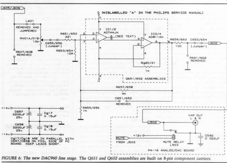
-------------- FIG. 6
In the last issue of TAA, we discussed modifying the DAC960 ( “POOGE-5: Rite of Passage For The DAC960, Part I, ” TAA2/92, p. 10). In Part II, we cover a new line stage.
Since Part I was written, Walt Jung and I have made a minor change on the PA16 DAC/output board's power sup ply bypassing. This change affects C855 and C856 in Procedure 4, as well as C571, C572, C573, and C574 in Procedure 5. These six capacitors were originally specified as 1000uF/25V Panasonic HFQ electrolytics. We've changed them to 2200 uF/25V Panasonic HFQs, Digi-Key part #P5716. The higher values offer slightly improved dynamics, with greater clarity and detail in heavily scored music passages. While taller, the larger value HFQs do not change the footprint size of the caps or make them any more difficult to install. On most systems, the audible change will be subtle, but worthwhile. You may find the change more apparent if the rest of your system is high resolution. (The Old Colony kits will include the 2200uF capacitors.) New Line Stage The DAC960's original preamp line stage is built around a pair of mediocre 5534 op amps, Q651 and Q652. (Q652 is mislabeled as Q651 in the manual).
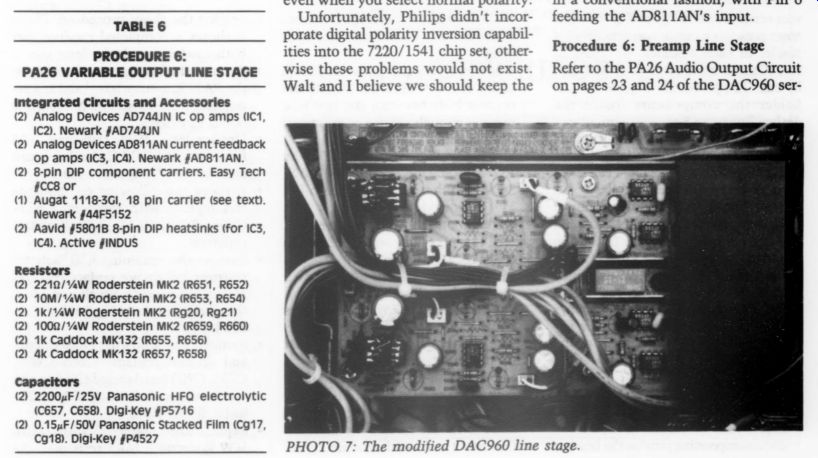
PHOTO 7: The modified DAC960 line stage.
-------------
TABLE 6: PROCEDURE 6: PA26 VARIABLE OUTPUT LINE STAGE
Integrated Circuits and Accessories (2) Analog Devices AD744JN IC op amps (IC1, IC2). Newark #AD744JN (2) Analog Devices AD811AN current feedback op amps (IC3, ICA). Newark FAD811AN.
(2) 8-pin DIP component carriers. Easy Tech #CC8 or (1) Augat 1118-3Gl, 18 pin carrier (see text).
Newark #44F5152 (2) Aavid #5801B 8-pin DIP heatsinks (for IC3, IC4). Active INDUS Resistors (2) 2210/vW Roderstein MK2 (R651, R652) (2) 10M/0.25 Watt Roderstein MK2 (R653, R654) (2) 1k/vW Roderstein MK2 (Rg20, Rg21) (2) 100 ohm/vaW Roderstein MK2 (R659, R660) (2) 1k Caddock MK132 (R655, R656) (2) 4k Caddock MK132 (R657, R658) Capacitors (2) 2200 uF/25V Panasonic HFQ electrolytic (C657, C658). Digi-Key #P5716 (2) 0.15 uF/50V
Panasonic Stacked Film (Cg17, Cg18). Digi-Key #P4527
------------
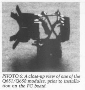
PHOTO 6: A close-up view of one of the Q651/Q652 modules, prior to installation on the PC board.
-----------
Philips chose the same quality passive components as elsewhere-unacceptable for high-end performance. Philips did, however, use a high-quality blue Alps pot for the volume control.
I decided early to dispense with the DAC960's pair of balanced outputs and the extra stage to invert absolute polarity. Because the balanced outputs are fixed and not controlled by the volume pot, they are of limited use. Cable runs between the fixed balanced outputs and the inputs to the preamp would be short enough to eliminate the need for balanced outputs. In addition, few pre amps have balanced line inputs. While these might be useful in broadcast applications, balanced line inputs serve no purpose for the majority of TAA readers.
The polarity inversion stage introduces its own set of sonic problems.
Even if you replace the op amps (you guessed it--5534s!) with high performance devices, the signal still passes through an extra stage when the polarity is inverted. The slight loss of resolution introduced by this stage will make it difficult to determine just what you're hearing. Is the change in sound caused by the polarity inversion, or by the extra stage of electronics? Relay L601's contacts are always in the signal path, even when you select normal polarity.
Unfortunately, Philips didn't incorporate digital polarity inversion capabilities into the 7220/1541 chip set, other wise these problems would not exist.
Walt and I believe we should keep the line stage's performance level as high as possible, which means keeping the signal path as simple as possible.
In the new line stage (Fig. 6), an Ana log Devices AD744JN-FET input op amp provides the circuit's gain, while an AD811AN transimpedance amplifier serves as a unity-gain high-current Class A buffer. The AD811AN operates inside the overall feedback loop. Walt described this circuit in his sidebar to Part I, as well as in the Analog Devices Seminar Notes he cited.
On the surface, this circuit appears similar to the buffered preamp line stage described in TAA 2/90, with different devices. A closer examination, however, reveals an important distinction-the AD744jN's output stage is bypassed and Pin 6 is not used. A frequency compensation pin, Pin 5, is located just ahead of the output stage.
Connecting the AD744jN in this fashion simplifies the signal path and pro vides Class A amplification in every stage without using pull-down resistors or a current source at the op amp's output.
The AD811AN's noninverting input impedance is over 1M, so you do not need to drive it from the op amp's push/pull output stage. As far as know, the AD744 is the only high-performance op amp which you can configure this way. If you wish to experiment with other op amps, you must connect them in a conventional fashion, with Pin 6 feeding the AD811AN’s input.
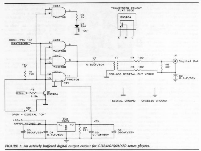
FIG. 7
Procedure 6: Preamp Line Stage
Refer to the PA26 Audio Output Circuit on pages 2.3 and 24 of the DAC96O service manual and to Fig. 6. The new line stage presents a minor construction obstacle: In each channel, we must fit two ICs in a space previously occupied by one. The procedure is quite simple:
Solder the components inside the dashed line to an 8-pin component carrier or header to form a small module that you can then solder into the existing PC footprint. In Fig. 6, I call these the Q651 and Q652 assemblies.
Select an 8-pin component carrier or header, an AD744JN, and an ADB811AN. (If you can't find 8-pin carriers, you can make a pair of them from one 18-pin carrier, as I explained in Part 1). Bend the thin portions of the AD744JN's pins out sideways until they are parallel with the top of the device. Bend the pins of the AD811AN the same way.
Solder Pins 1-4 of the AD744jN to the corresponding pins on the carrier, so the op amp sticks straight up.
Solder Pins 5-8 of the AD811AN to the corresponding pins on the header, the IC sticks straight up. The bases of the two ICs should now face each other.
Solder a 1k resistor between Pins 2 and 6 of the AD811AN. Situate the resistor body between the two ICs, leaving enough clearance to install the heatsink.
Solder a jumper between Pin 7 of the AD744jN and Pin 7 of the AD811AN.
Solder another jumper between Pin 4 of each device.
Solder another jumper between Pin 5 of the AD744JN and Pin 3 of the ADS811AN.
Make sure the IC pins do not touch one another. Be especially careful you do not create any solder bridges between the component carrier pins.
The jumpers and the resistor must clear each other.
Slip an Aavid-5801B 8-pin DIP heat sink over the AD811AN. Make sure none of the leads touch the heatsink, and the 1k resistor doesn't interfere.
Construct a second module by re the above procedure. Photo 6 shows a completed module. Set both modules aside for later use.
Remove the black metal shield from the PA26 line stage board and any remaining Phillips screws holding the board in place.
Unplug J502, J503, J505 and J506 from the PA16 DAC/Analog board and lift the PA26 board out.
Remove the following components and replace with jumpers: C653 C656, R663, R664 (3.3 ohm “safety ” resistors).
Remove the remaining 3.3 ohm “safety ” resistors but do not replace (this removes DC power from all non-functional circuitry): R611, R612, R751, R752-R754.
Remove the following components and do not replace: C603-C606, C701, C702 (mislabeled C655 in the service manual) C651, C652, R607 R610, R661, R662.
Replace R651 and R652 with 2210/0.5W Roderstein MK2 resistors.
-----------------
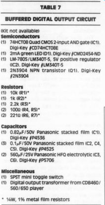
TABLE 7 (Kit not available)
Semiconductors (1) 74HCT08 Quad CMOS 2-input AND gate (IC1).
Digi-Key #CD74HCTOSE (1) 2mA green LED (D1). Digi-Key #CMD2454-ND (1) LM-7805/LM340T-5, 5V positive regulator (IC2). Digi-Key #LM340T-5 (1) 2N3904 NPN transistor (Q1). Digi-Key #2N3904 Resistors (1 10k RD*
1) 1K (R2*
1) 2.2k (R3* (2) 100 ohm (R4, RS)* (2) 2210 (R6, RN ”
Capacitors (1) 0.82 uF/50V Panasonic stacked film (C1).
Digi-Key #P4536 (3) 0.14F/50V Panasonic stacked film (C2, C4, CS). Digi-Key P4525 (2) 560 uF/25V Panasonic HFQ electrolytic (C3, C6). Digi-Key #P5706 Miscellaneous (1) SPST mini toggle switch (1) Digital output transformer from CDB460/ 560/650 player
0.5 W, 1% metal film resistors Replace R653 and R654 with 10M/0.25 Watt Roderstein MK2s.
Replace R659 and R660 with 10 0 ohm/ 0.25 Watt Roderstein MK2s.
Replace R655 and R656 with 1k Cad dock MK132 resistors.
Replace R657 and R658 with 4k Cad dock MK132s.
Replace C657 and C658 with 2200uF/25V Panasonic HFQ electrolytic capacitors in parallel with 0.15uF Panasonic Stacked Film caps.
The 0.15 uF caps should be soldered to the foil side of the board.
Remove relay L601. Install two jumpers in the middle pairs of holes left vacant when you removed the relay to bypass the polarity inversion stage and eliminate the relay contacts in the signal path. Leave the four outer holes empty.
Remove Q651 and Q652 and replace them with the two modules already constructed. The module's orientation is important. Pins 1 and 8 of the modules (and, therefore, the ICs) must face the DAC960's front panel.
Make sure the heatsinks don't touch any PC-board hardware.
Photo 7 depicts the modified PA26 board with the IC modules installed.
After checking your work carefully, re-turn the PA26 board to its original placement. Make sure no wires are pinched under the board. You no longer need the large metal shield; it formerly pro vided additional shielding for the balanced output transformers we are no longer using. Reconnect all the cables and check the line stage for proper operation, preferably with a CD test disc and an oscilloscope. If you have a harmonic distortion analyzer, check the THD, as well. With the volume set for a 2V RMS output, the distortion readings should be nearly identical to the fixed outputs (see Part 1).
Check the DC offset: With the volume control at minimum, DC at the variable outputs should be less than +5mV RMS. As the volume control rotates clockwise, the offset normally increases, since the offset from the BUF03 is now added to that of the line stage. With the volume at maximum, the offset may be as high as +-35mV.
Because the line stage is well into hard clipping with a digital 0dB signal at this point, you'll never actually run the volume this high. My DAC960's left and right channels output offset measure +30mV and + 15mV, respectively, just below clipping. This offset level shouldn't be a problem with most power amps. If you use a power amplifier with a gain at DC (most power amps are actually unity gain at DC- they don't amplify direct current), use ...
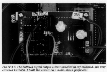
PHOTO 8: The buffered digital output circuit installed in my modified, and very crowded CDB650. I built the circuit on a Radio Shack perfboard.
... a power amp with an input coupling capacitor. Without going into an elaborate discussion of this line stage's sonic characteristics, let it suffice to say the comments I made on the improvements described in Part I apply here, as well. (Old Colony may offer a complete parts kit for Procedure 6, as well.) For some time, I've used a preamp line stage similar to the one I described in TAA 2/90, the only difference being replacing AD744jNs with the Linear Technology LT1056s, and lowering the bias resistors on the LT1010 buffers to 330, so the output stages run very rich Class A. When compared with the modified DAC960, I prefer the DAC960 over that preamp's line stage. Using the AD811AN as the buffer results in greater inner detail and resolution. Overall, the sound is cleaner and more 'open.' Un fortunately, my variety of source material requires a preamp with analog in put switching. I plan to replace the line stage in my preamp with the modified DAC960 circuit.
--------------
REFERENCE
1. Galo, G. “Ask TAA, ” TAA 2/90, p. 48, Fig. 1. Aavid Engineering, Inc.
PO Box 400 Laconia, NH 03247 (603) 528-3400
----------------------
ACKNOWLEDGMENT
I'd like to thank Mr. Jeffrey Divers at Aavid for his help in sending us heatsink samples for the DAC960 project. If you have any heat sink needs, I highly recommend contacting Aavid.
--------------
One or two of the modified line stage's limitations I did not address have to do with the quality of the DAC960's internal wiring. First, the wiring harness carrying the regulated supply voltages from the PA16 board to the PA26 board is flimsy-Philips used 22AWG wire. You would definitely find further improvement by replacing the +14V, -14V and ground lines with heavier wire. This may be tricky because Philips doesn't leave you much room to work on this PC board. Fortunately, the low Z 2,200uF HFQ local bypassing capacitors help to overcome the wiring deficiencies.
The second limitation is the wiring carrying the audio signals between the PA16 board and the volume pot, the volume pot and the PA26 board, and the cable from the PA26 board back to the variable output jacks on the PA16 board; it is of 'dime store’ quality. Unfortunately, Philips also uses many plug-in connectors along the way.
Whether you hear any problems will depend upon the rest of your system's resolution.
You may wish to consider replacing all of the internal wiring with better cable. Mogami 2534 would be a good choice. You probably won't be able to re-use the Philips plug-in connectors, although it's just as well. Again, soldering new wiring to the Philips boards will be tricky; you'll have to decide whether changing the power supply and signal cables merits the extra effort.
(The Old Colony kits won't include wiring upgrades.)
A Few Extras
While possibly of limited interest, I'd like to share two other circuits and have included parts lists for these projects. Resistor types aren't critical for these circuits: You can use the resistors sold by Old Colony, or the Yageo 1% metal film resistors from Digi-Key.
The digital outputs on the CDB460/ 560/650 series, as well as many later Philips CD players, leave much to be desired. If you look at these player's digital output waveforms, you'll find a visible distortion or tilt-quite a contrast to the perfectly rectangular pictures in Philips' service manuals. Walt suggested replacing the original digital output in my CDB650 with the circuit shown in Fig. 7. In the original con figuration, the DOBM signal from the SAA7220 digital filter feeds the digital output transformer directly. The new circuit buffers this signal with three paralleled sections of a 74HCT08 Quad AND gate. The fourth section of the chip drives a low-current CMOS-compatible LED that glows when you switch the digital output on.
Some CD players with buffered dig ital outputs may benefit from this up grade. Unfortunately, Philips used paralleled sections of a Quad TTL chip in some of their higher priced players.
Visible waveform distortion shows up on these outputs, as well. You can parallel CMOS sections without problems but you shouldn't parallel TTL sections. If your player shows visible digital output waveform distortion, you should consider this upgrade. The popular Rotel CD855's buffered digital out put also benefits from this change, al though you may choose to simply up grade the existing circuit over whole sale replacement.
------------
If there is sufficient interest, Old Colony Sound Lab will offer the following products:
New DAC960 (less than original retail price) . . . .
Kit of parts for Procedures 1-5
Both the DAC960 and the Procedure 1-5 Kit
A Kit of parts for Procedure 6
Indicate your nonbinding preference by writing the appropriate number on your Fast Reply card.
--------------------
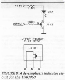
FIGURE 8: A de-emphasis indicator circuit for the DAC960.
Head Set
You can build this circuit on a small perfboard or piece of Ivanboard. Photo 8 shows my circuit mounted in my CDB650 with a custom-fabricated aluminum bracket. You must remove the digital output transformer from the main PC board of your 650-type player and mount it on the board containing the new circuitry. Except for the output jack (J1), you should mount all parts on the small perfboard. An unregulated + 10V should be taken from the 650's power supplies. The output terminal of the 7805 regulator, C5 and C6 must be as close as possible to the 74HCT08 so the lead length between the SAA7220 and the perfboard is as short as possible.
---
TABLE 8
DE-EMPHASIS INDICATOR
(Kit not available)
(1) Siliconix J-112 N-channel JFET. Active #19080
(1) 2mA Green LED. Digi-Key #CMD2454-ND
(1) 1.5k ohm
(1) 100k-ohm
0.25 Watt , 1% metal film resistors
----------
The kill line is the same one which activates the analog muting circuit.
This line is designated as test point 93 in the CDB460, 473, 560, and 650 ser vice manuals. The same kill line is also shown in the CDB582 service manual, although the 582 doesn't have any digital output (the DOBM line on the SAA7220P/B digital filter is unused).
You can still add this circuit even if your player doesn't have a digital out put, as long as you use a digital output transformer. The one in the players I mentioned is part no. 4822-148-80281.
You can order a transformer by calling NAP Consumer Electronics' Parts Dept. at (800) 851-8885 or (615) 636-5859.
You can mount both the output jack and the digital on/off switch on the CD player's rear panel. When using the CD player as a standalone unit without an external D/A converter, switch the dig ital output off. Finding a place to mount the LED can be a problem, but because I don't use the headphone amp on my CDB650, I mounted the LED inside the headphone jack.
Be sure to remove the harness connecting the headphone jack to the “additional filtering” board--I scrapped the “additional filtering” board years ago.
Solder a pair of thin (20 or 22AWG) wires to the LED, making note of polarity, and cover the leads with heat shrink tubing. Insert a small screwdriver into the front of the headphone jack, and push it straight through. This will break off the small piece of plastic covering the rear of the jack. Next, insert the small leads and pull the LED through until seated inside the headphone jack. It's a neat fit, and looks terrific with active digital output. This circuit should be easily adaptable to any Philips/Magnavox player with a SAA7220P/A or P/B digital filter.
Accentuate the Positive
Did you ever wonder which CD manufacturers actually use pre-emphasis in their CD mastering? Walt and I included a circuit to indicate when the de-emphasis circuit is activated. Figure 8 shows the simple de-emphasis indicator. I built my circuit on a small piece of Ivanboard and mounted it near the digital power supply board (Photo 9). It is held in place with the digital supply's corner mounting screw. I cut the Ivan board to fit around the neighboring cop per heatsink. The + 14V analog supply rail is connected to a low current LED in series with a Siliconix J-112 FET.
When the de-emphasis line rises to +0.7V, the gate turns the JFET and LED lights on.
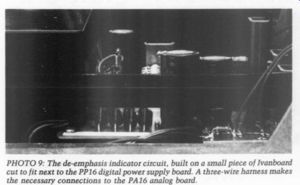
----------- PHOTO 9: The de-emphasis indicator circuit, built on a small
piece of Ivanboard cut to fit next to the PP16 digital power supply board.
A three-wire harness makes the necessary connections to the PA16 analog board.
You can mount the LED inside the DAC960's headphone jack after un soldering the PE26 board's three-pin connector. Then, fit a piece of heat shrink tubing over this connector. Solder the 22AWG wires to the LED and cover them with heat shrink tubing, as indicated in the above digital output modification. You can unsnap the jack's clear plastic side piece, which will al low you to slip 22AWG wires through.
Once the LED is resting in place, the plastic side piece on the headphone jack can be snapped back into place, firmly holding the wires.
The DAC960 modification project has been an extremely rewarding one for Walt and myself, both educationally and sonically. I hope readers gain as much from the project as we have. Let us know how you fare with your own DAC960 modification. Please send any comments to me c/o TAA. May the POOGE be with you!
Also see:
POOGE-5: RITE OF PASSAGE FOR THE DAC960, A TWO-PART SAGA, part 1