By Hank Zumbahlen
This four-part article describes a high-performance outboard digital-to-analog converter (DAC) that you can build. The first part describes the design of the digital section, the second the analog section, the third the construction of the DAC, and the final part describes an optional optical receiver you can add to receive either TOSLINK or ST format digital data.
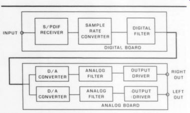
FIGURE 1: DAC block diagram.
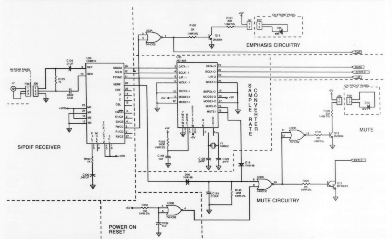
FIGURE 2: AES/EBU interface and rate conversion.
This converter uses a specific integrated circuit that is also a digital-to analog converter. To try to minimize the confusion, I will refer to the integrated circuit as a D/A converter, and to the overall project as a DAC.
The DAC also uses a special asynchronous sample rate converter (ASRC) chip, the Analog Devices AD1893, in the digital section of the receiver.
The ASRC's primary design purpose is to change the sample rate in real time, allowing digital audio signals to be combined even if they are of different sample rates. The ASRC allows the input sample rate to be anywhere from 25-60 kilo-samples per second (KSPS).
(Of the three main sample rates in digital-audio use, the most common is the 44.1 KSPS, the rate of the compact disc. Next is the 48 KSPS of digital audio tape (DAT).
Finally, 32 KSPS is used in film and direct-broadcast-stereo (DBS) radio.) The DAC uses the ASRC chip for a different purpose: to present a uniform sample rate to the D/A converter (and the reconstruction filter) with different input sample rates. (The reduction of jitter is a happy side effect of the rate conversion process; see sidebar.) Failing this uniform rate, you would have to modify the response of the reconstruction filter for the different data rates to preserve maximum performance. The ASRC greatly simplifies the design of the filter.
The Receiver
Figure 1 shows a block diagram of the DAC. The DAC's input is an S/PDIF (Sony /Philips Digital Interface Format) or AES/EBU (Audio Engineering Society/ European Broad cast Union) signal. This receiver uses the 75-ohm unbalanced termination of the S/PDIF format rather than the 100 ohm balanced termination of the AES/EBU format. Part 4, which deals with input format options, will describe conversion to the AES balanced format.
For commercial applications, the standard connector for this interface is the common RCA phono jack. Optionally, you can make the connection through an optical fiber. (This option will also be discussed in Part 4.) The professional implementation of the AES/EBU interface uses an XLR-type connector, with a balanced input line.
The base unit is designed with the most common configuration-the standard consumer interface-with the other input configurations as options.
The signal arrives at the digital board where it is terminated, matching the line impedance, to reduce reflections in the cable, another potential source of jitter. The signal is then passed on to a specialized receiver chip. The circuit contains the phase locked loop that recovers the individual signals of the composite AES signal; see sidebar. These signals are then transmitted to the appropriate separate pins of the ASRC chip. The receiver also strips off the control information in the "header." This control information details the length of the data word-which can be up to 20 bits for professional applications-the sample rate (32kHz, 44.1kHz, or 48kHz), whether the optional pre-emphasis is used, whether the signal is a digital copy (the infamous copy-code protection), and several other items of data. This design uses only the emphasis indication and a signal that mutes the output of the DAC should there be an error in the received signal, or no signal at all. Both these signals are also available as front-panel indications. For a complete description of all of the components of the AES and S/PDIF signals, refer to the sources listed in the bibliography.1.23 There is a potential problem in inter facing the AES receiver to the ASRC.
Since the AES format allows greater than 16-bit resolution, the data frame must be larger than 16 bits. Because it's convenient to use lengths that are binary numbers, the data frame is 32 bits wide, so your 16-bit signal will occupy only half the available time slots.
There is no standard as to which half of the slot it uses. The data can occupy the first half, with the second half at logic 0, or the second half, with the first half at logic 0. The former is left-hand justification and the latter right hand justification. You can program the receiver chip and the 1 ASRC for either justification, but " the interpolation filter requires right-hand justification, so you adopt this as the standard in this design. The schematic of the input receiver is shown in Fig. 2.
The Sample-Rate Converter
The next block is the sample-rate converter. As mentioned earlier, the ASRC is a specialized digital signal processor, using a very innovative method of changing the data rate. You might think of it as a digital filter whose coefficients vary on a sample-by-sample basis.
On the input side you have the output of the receiver, and on the other side the output of a crystal controlled clock and a frequency divider string. This oscillator string provides you with an extremely accurate and, more importantly, stable (low jitter) clock. The received samples are transmitted to the digital filter.
A separate circuit compares the edges of the input and output L/R clocks to determine which of the digital filter's 65k coefficients to use. All these coefficients are of the all-pass form, which means that the frequency responses are all equal, varying only in the amount of group delay.
The difference between the edges of the input and output clocks determines the amount of delay. Less delay is added if the clocks are widely separated, more if they are close. The output of the filter is the new audio data at the new data rate. Figure 3 is a block diagram of the ASRC.
This simplistic explanation of the internal workings of the ASRC is given for easy understanding. For a more detailed explanation, refer to the sources in the bibliography.-8.9:10
Using the ASRC to standardize the output-data rate optimizes the performance of the reconstruction filter. In designing the filter, it is important to make sure the passband is as wide as required, but no wider. You need to ...
---------
TABLE 1
PARTS LIST
-------------
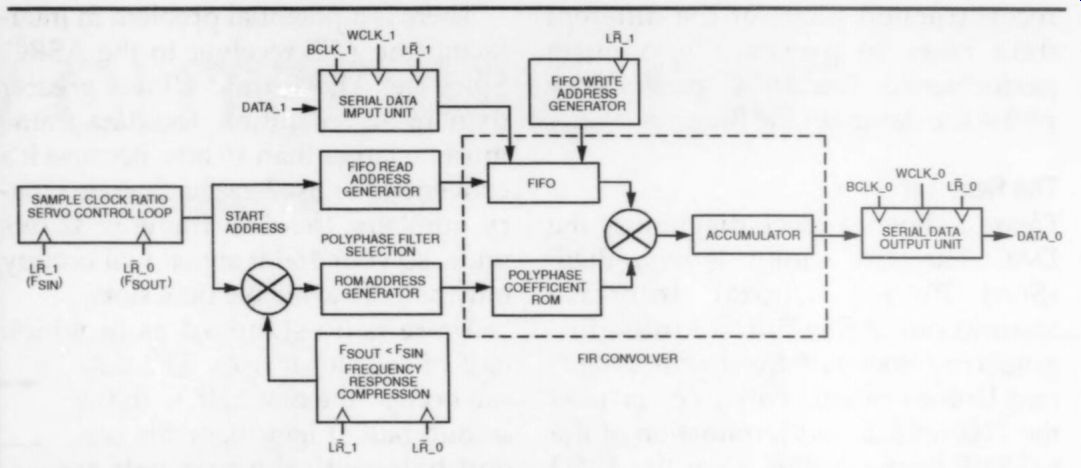
FIGURE 3: AD1890/AD1891 functional block diagram.
... pass a 20kHz signal with no attenuation, yet have as much attenuation as possible of the image frequencies, which will be centered around the new sample rate of 384 KSPS (eight times oversampling of a 48 KSPS data rate).
Without the ASRC, if you design the reconstruction filter around the CD sample rate of 44.1kHz, it slightly restricts the bandwidth of the 48 KSPS signal. Alternatively, designing around 48 KSPS loses some attenuation to the images around 352kHz, which is eight times 44.1kHz. Admittedly, these differences are small, but they are nonetheless real. A bigger difference exists with 32 KSPS signals, where the bandwidth must be limited to 15kHz and the images are now centered at 256kHz.
++++++++++++++++
Background
When the compact disc appeared in the early 80s, it promised "perfect sound for ever." While it is true that the storage media was noise free, limitations in the associated conversion hardware precluded the full realization of this promise.
One limitation of the analog-to-digital conversion process is that the bandwidth of the input signal must be less than half of the sampling rate. This is called the Nyquist criterion. Allowing frequencies outside of this band at the input of the converter will result in an "alias," which is the reflection of the input frequency off the sample rate.
For example, if you were to choose the standard sample rate of 44.1 KSPS and allow an input frequency of 30kHz, it would show up as a 14.1kHz (44.1-30) signal. Then, once digitized, this signal would be in the band and impossible for you to remove. It looks exactly like a valid input, but it is not.
The highest audio frequency of interest is 20kHz. Therefore, a very complicated filter is required to limit the spectrum of the input to the converter. This filter must attenuate the input by 96dB (for true 16 bit performance) for signals greater than 22.05kHz while passing 20kHz signals with no attenuation. (This, by the way; is one of the main reasons for the popularity of the sigma-delta [ZA] conversion technique. By using high values of over sampling-typically 64-384 times the sample rate-the order of the antialiasing filter is reduced significantly.)
Reconstruction Filter
A similar filter is also required in the playback circuits to smooth output from the digital-to-analog (D/A) converter chip. This, known as the reconstruction filter, converts the "stairstep" output of the converter to a smoothly varying waveform by eliminating the high-frequency components.
The first generation of CD players used "brick wall" reconstruction filters after the D/A chip. These filters tended to "ring" due to the high Q sections required by their high order (number of stages)-in some cases 12th order or more. The ringing shows up as what appear to be spurious oscillations on the waveform, especially on fast edges.
The first "fix" to the CD format was the adoption of oversampling. Inserting a filter in the digital domain ahead of the D/A converter and using interpolation--a digital-signal processing technique by which the sample rate of the converter is effectively increased-served to reduce the order of the analog filter. This was an advantage for both the consumer and the manufacturer. The high-order filter was gone, along with its inherent response problems, such as ringing and ripple in the passband. A lower-order filter was also less expensive to design and manufacture.
--------------------------------
The industry quickly moved to four times oversampling, while some higher end systems moved to eight times oversampling. Although some designers escalated the oversample rate past the point of diminishing returns, most systems settled on a standard of four or eight times.
The digital section of the player also evolved. Boards full of integrated circuits gave way to a small number of VLSI (very large scale integration) chips in specialized sets. This both improved the reliability of the player and cut the cost drastically.
While this evolution in the digital section was taking place, the analog section remained fairly static. In most cases, the reconstruction filter was standardized to third order. This represented a reasonable compromise between performance and complexity.
Separating Functions
Finally, a separation of the functions of the CD player took place. Just as the preamplifier and power amplifier were separated for maximum performance, so, too, were the player's servo positioning system and the digital-to-analog conversion function. This last separation required the adoption of an interface standard. This standard is either the AES/EBU (Audio Engineering Society /European Broad casting Union) standard for the connection of Digital Audio components,-- or the S/PDIF (Sony /Philips Digital Interface Format). [3] (Sony and Philips, by the way, are the co-inventors of the CD format.) The AES/EBU format is generally used in a balanced configuration for profession al applications, although there is a single ended option. The S/PDIF format is single-ended and more common in consumer applications. Otherwise the two standards are very close, differing mainly in level and input impedance.
The standard digital-audio signal set consists of four signals: the audio data, which alternates between left and right channels; a clock equal to the data rate; a clock to identify whether it is the left or right channel; and, in most cases, a clock to identify the completion of one word or complete set of signals for each channel.
To minimize both the number of connections between two separate pieces of equipment and the effects of skew (timing differences) between the signals, all four are combined into one signal for transmission. At the receiving piece of equipment, the signals are separated back into their original form.
Jitter
The process of separating the signals gives rise to a form of distortion known as jitter. The standard method of recovering the signals uses phase-locked loops to recon struct them. You can design a phase locked loop either for great stability or wide capture range, but it is very difficult to design it for both. In most cases, you must optimize capture range to make sure the loop acquires and holds lock. Obviously, if the loop does not lock, it can recover no data. But this means that the frequency of the loop will be less stable and can wander around a bit, which causes slight variations in the width of the re covered clock pulses.
At the D/A converter, movement of the word clock, which actually changes the information the D/A responds to, causes jitter. An easy way of visualizing this concept is to remember that the right signal at the wrong time is a wrong signal (Fig. 6). This example is exaggerated, but it may help to get the point across. [4-6]
Early designs of this DAC used dual phase-locked loops to reduce the jitter. The first loop was designed to maximize capture range, whereas the second was designed to achieve higher stability. Since the first loop kept the frequency input to the second relatively constant, the second could be optimized for stability of the output timing. A second way to accomplish this became available when Analog Devices released its asynchronous sample rate converter (ASRC) chip.
++++++++++++++++
No one filter can optimally accommodate the requirements of these different sample rates. However, using the ASRC standardizes the output-data rate at 48 KSPS no matter what the received data rate-as long as it is within range, of course--and optimizes the performance of the reconstruction filter. A side note about 32 KSPS: while not in widespread use at this time, it should become more prevalent with the growth of DBS (direct broadcast satellite) FM and TV.
As mentioned above, another advantage of using the ASRC is the reduction of jitter in the signals presented to the D/A converter. The audibility of jitter is still a hot issue in the audio community. The effects of jitter are subtle--an increase in both distortion and the noise floor--but as performance levels improve, the importance of even subtle forms of distortion increases. Figure 2 shows a schematic of the ASRC section.
The Interpolation Filter
The last section of the digital board is the interpolation filter, which is another specialized digital signal processor chip. From the ASRC, it takes in a 16 bit digital-audio string at, in this case, 48 KSPS, and through the process of interpolation, adding samples, and averaging, it outputs a digital-audio string at eight times the sample rate (384 KSPS) and 20-bit resolution.
The right- and left-channel information is output to separate pins to reduce the speed requirements of the serial output ports. Low-pass filters are added to each line that goes to the analog board to limit the bandwidth of the signal, which in turn reduces the HF noise caused by coupling of digital noise into the D/A converter. Figure 4 shows the schematic for the interpolation filter.
---------------
------------
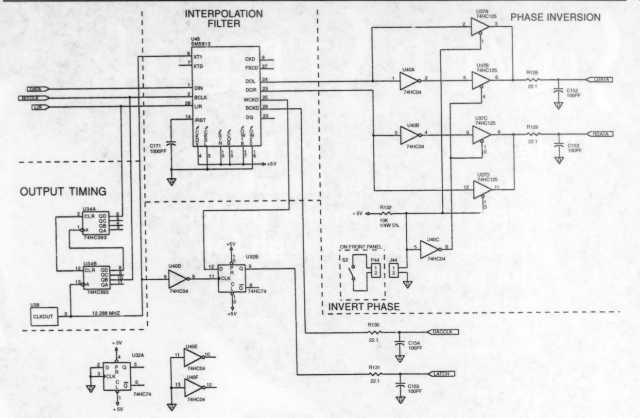
FIGURE 4: Interpolation filter.
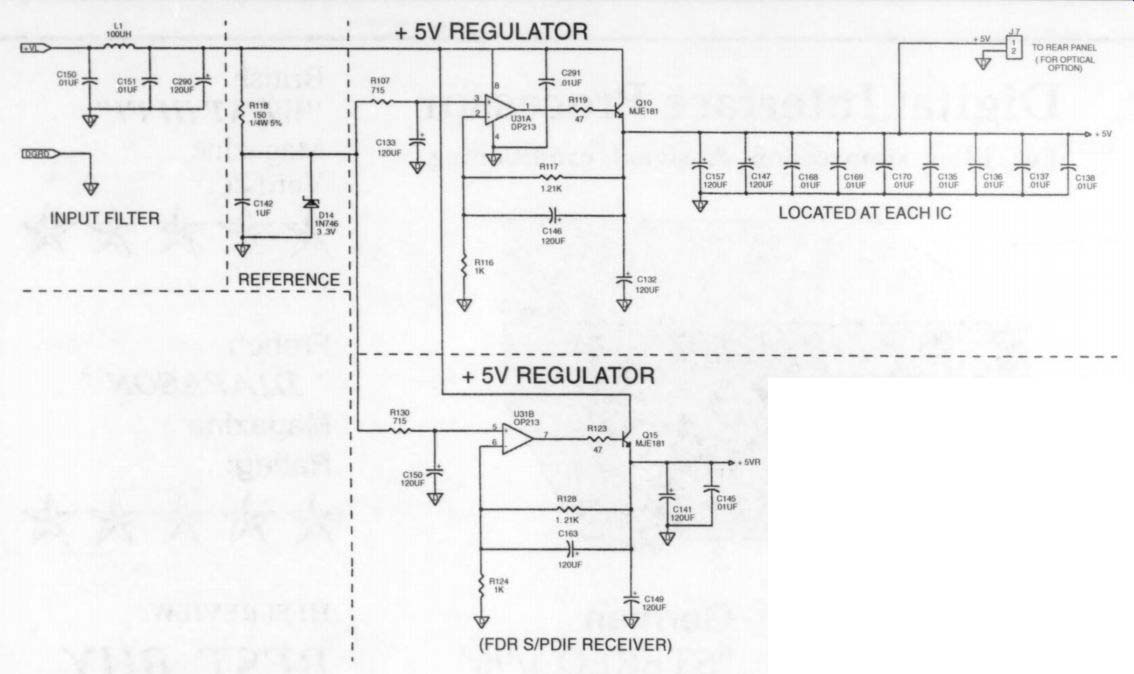
FIGURE 5: Digital regulator.

FIGURE 6: The effect of Jitter.
Other Circuits
There are a couple of other circuits resident on the board. The first is the output mute circuit, which shorts the output of the DAC's analog section on power-up and in the event of an error. Two possible sources of error are loss of input signal and input frequency out of range. Both these conditions are detected in the AES receiver chip.
There is also a remote possibility of sample overrun in the ASRC. If this occurs, the ASRC chip outputs an error signal that is combined with a power delay to short the output so undesirable noises won't assault your ears. A front-panel indicator of the mute condition is provided.
Another front-panel indicator shows whether or not emphasis is on. An optional pre-emphasis and complementary de-emphasis were defined in the CD format. The idea was to provide the pre-emphasis for classical music, but not for rock. In my experience very few CDs use emphasis, so don't look for this light to come on very often. Whether or not the emphasis is on is contained in the header of the digital-audio signal, and the AES receiver chip detects it.
Another circuit provides the ability to invert the phase of the output signal--also a hotly debated subject in audio. Some think that the wrong polarity can inhibit the ability of a system to project a convincing image.11 Whether this effect is audible is debatable, especially since only a small amount of source material takes phase integrity into account. The ability to invert the phase via a front-panel switch is included for those instances when you desire it.
-----------
SOURCES
Allied (800) 433-5700
Asgard Audio
660 Rebecca Dr., Boulder Creek, CA 95006
(408) 338-2954 Digi-Key 701 Brooks Ave. S., PO Box 677 Thief River Falls, MN 56701-0677 (800) 344-4539
Mouser Electronics (800) 346-6873
-----------
Power Supplies
One of the most overlooked areas of audio design is the power supply. The usual practice is to use commercial three-terminal regulators, such as the LM78XX family. These devices are easy to use and provide good performance at DC and low frequencies. The problem is that the op amps used in the control sections of these regulators have limited bandwidth.
The output impedance of the regulator rises with frequency, which is an issue because it is desirable to have as low an impedance across as wide a frequency as possible, thus helping to limit high-frequency noise. The design of the regulator in this DAC is based on the Sultzer circuit, as modified by Jung, and is basically a discrete implementation of the monolithic regulators, using higher bandwidth active components.
This regulator and the copious use of decoupling capacitors provide as solid and noise-free a voltage source as possible. The schematic of the regulator is shown in Fig. 5. Note that a separate regulator section is provided for the AES receiver chip. The PLL aspect of this chip is more analog than digital in nature, and it's advantageous to isolate it from the rest of the digital section and its inherent noise.
Conclusion
This concludes the design of the digital board. In Part 2, I'll discuss the design of the analog section. Table 1 is the parts list of the digital board. Note that special emphasis has been given to making the parts available to individuals. Kits of semiconductors and boards are available from the sources listed.
++++++++++++++
REFERENCES
1. Audio Engineering Society, "AES Recommended Practice for Digital Audic Engineering-Serial Transmission Format for Linearly Represented Digital Audio Data," AES 3-1985 (ANSI S4.40-1985).
2. Sanchez, Clifton & Taylor, "Overview of Digital Audio Interface Structures," Crystal Semiconductor Application Note AN22.
3. International Electrotechnical Commission, "International Standard Digital Audio Interface," IEC 958, 1989.
4. Hartley, R., "The Jitter Game," Stereophile, Jan. 1993.
5. Fourre, Remy, "Jitter and the Digital Interface," Stereophile, Oct. 1993.
6. Fourre, Remy, "Jitter, Jitter, Jitter...," UltraAnalog Inc. Ap. Note AP-103.
7. Adams, Bob, "Clock Jitter, D/A Converters, and Sample-Rate Conversion," The Audio Critic, Issue 21.
8. Adams, R., "The Theory and VLSI Architecture for Asynchronous Sample Rate Converter," JAES, Oct. 1992.
9. Wood, Maury, "An Integrated Circuit Asynchronous Sample Rate Converter for Professional Audio Application," Analog Devices
10. Adams, Bob, "Asynchronous Sample Rate Converter," Analog Dialog, #28-1.
11. Johnson, R.C., The Wood Effect, The Modern Audio Association, 1988.
12. Sultzer, M., "A High Quality Power Supply Regulator for Operational Amplifier Preamplifiers," TAA 2/80.
13. Jung, Walt, "Regulators for High Performance Audio," TAA 1/95.
Also see: