In the midst of the digital revolution, here is an analog audio power meter, using all analog components, including a d'Arsonval meter. With a little redesign you can make it a true RMS audio voltmeter.
The meter movement I used in my prototype power meter is the one Old Colony supplied with its DC-10 capacitance tester (no longer available), which I never built because low-cost, accurate, digital capacitance meters are now readily available. I kept looking for a project for that large (4.5" x 6") Modutec PA3 panel meter, and here it is. The parts cost (excluding the chassis) is about $105.
How It Works
A block diagram of the Audio Power Meter is shown in Fig. 1. Photo 1 shows the completed unit, and Table 1 is the parts list. The meter is connected between the audio amplifier under test and its test load, typically 4 or 8-ohm power resistors, using J2-J5. The power meter senses the voltage across the amplifier output terminals and inserts a low resistance (50 m-ohm) in series with the load, which allows the amplifier current to be sensed and amplified 20 times (U3b).
The voltage and current are applied to input attenuator/amplifiers (U3a, U3d), with switching (S 2) that provides six power ranges from 1W to 300W.
The signals representing the amplifier's voltage and current are multiplied in an analog multiplier IC (U4), which produces an output signal that is one-tenth the product of the two input signals.
This output signal is then amplified and calibrated (U3c), and sent to an RMS-to DC converter IC (U5) that creates a DC voltage proportional to the RMS value of its input signal.
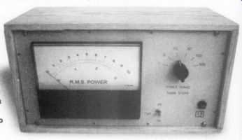
PHOTO 1: The Audio Power Meter.
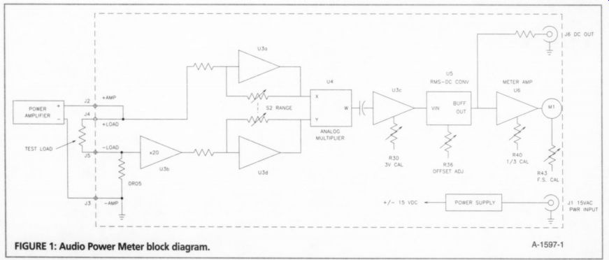
FIGURE 1: Audio Power Meter block diagram
The RMS output, calibrated to 3V DC full scale, is sent to J6. This signal, which can be numerically correct for the 3W, 30W, or 300W ranges, is then read with a digital multimeter. (It does not provide a properly scaled signal for the 1W, 10W, or 100W ranges because that full-scale output level is 3.16V DC.) The output of the RMS-DC converter is also sent to the meter amplifier circuit (U6), which is a voltage-to-current (V-I) converter that scales the full-scale output to 1 mA on the "3" ranges, or 1.054 mA on the "1" ranges. This is compatible The meter amplifier also limits the maximum meter current to just over 1.1mA to prevent damage if high power is inadvertently applied to the meter in the 1W range. In fact, the entire meter circuitry is designed to continuously withstand 300W of power in the 1W range, and up to 625W for a few seconds, without damage.
Circuit Description
The schematic for the power supply is shown in Fig. 2. Power for the unit is obtained from a 15V AC, 0.4A plug-in power adapter, so no high voltage is present inside the unit. The 15V AC supply at J1 is dual half-wave rectified to +-21V DC. Ferrite-bead FB1 and C1 filter the rectification noise from CR1 and CR2.
Capacitors C2 and C3 filter the rectified DC applied to linear regulator ICs U1 and U2, which provide the +-15V DC power-supply rails. C4 and C5 further filter the output of the regulators. In addition, the supply rails to ICs U3-UG6 are locally bypassed with 100nF ceramic caps.
The meter uses a single-point star-ground connection at the perfboard power-supply ground point, thus preventing any ground loops in the meter signal path.
LED 1 provides the power-on indication for the meter when S1 is on, and fuse F1 protects the power adapter. You may notice that the LED is powered from the -21V DC. I did this to equalize the current in the positive and negative supply and to balance the flux in the AC power-adapter transformer. The LED draws about -13mA to achieve the desired brightness. R1 adds +4mA to the +7 to +10mA meter-amplifier-circuit current (VR1 and M1 in Fig. 3). so the positive rail current equals the negative rail current under most operating conditions.
Figure 4 shows the input attenuator/ amplifier and analog multiplier circuitry.
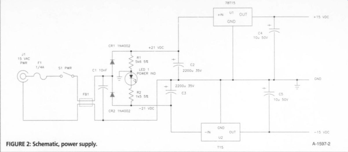
FIGURE 2: Schematic, power supply.
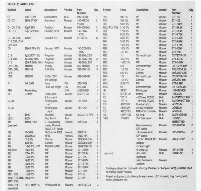
TABLE 1: PARTS LIST
The positive power-amplifier speaker terminal is connected to J2, and the amplifier voltage to the load is sensed at J4. Op amp U3a is an inverting amplifier used to amplify or attenuate (depending on the power range selected) the voltage signal. R3, in conjunction with one of the resistors R5-R10 on range switch S2A, sets the gain for U3a. R4 equalize the input bias currents for U3a, minimizing the input offset voltage error. C6 provides stability by rolling off the frequency response above 200kHz (1W range).
Protecting the Input
Since I designed the meter for input voltages as high as 499V RMS (300W into 8), CR3 and CR4 are used to protect the inverting input to U3a in case a high level of voltage is applied to the meter with S2A in the 1W range. R3 is sized to momentarily withstand power levels as high as 70V RMS, or 625W into 8-ohm.
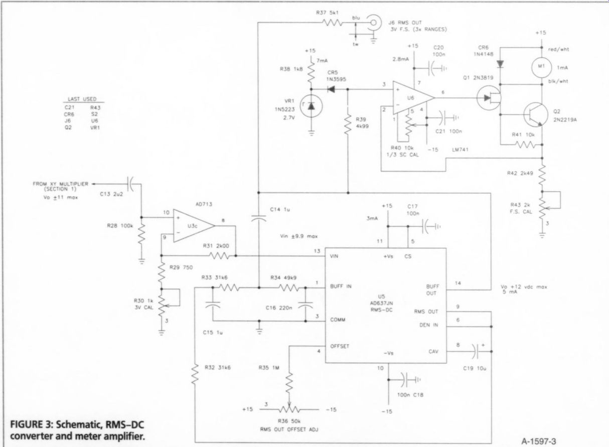
FIG. 3
The amplifier test load is connected between J4 and J5, and the negative power amplifier speaker lead connects to J3. A set of parallel resistors, R13 and R14, senses the amplifier current. These are 0R1 ohm, 1%-tolerance noninductive power resistors rated for 10W each. The resulting resistance is 0R05 ohm, which rep resents a 1.25% error with a 4 ohm test load.
You can easily compensate for this during calibration. (I used two 0R1 resistors because I had them on hand, but you can substitute a single 0R05 ohm resistor ( Newark p/n 96F6730 R0.05) for the two shown in the parts list.) The chassis ground connection for the circuitry is at the amplifier negative speaker jack, J3.
When I started this project, I intended to use the Unitrode UCC3926 current sensing IC'~3 because it has an internal shunt of only 1.3 m-ohm. However, after running some tests with the UCC3926, 1 found that the output waveform with a sinusoidal current is not a sinusoid (Fig. 5), and would not produce accurate results with the next stage of the meter, the analog multiplier. The "fuzz" at the peak of the UCC3926 current-output waveform in Fig. 5 is non-common-mode chopping noise from its chopper-stabilized current-sensing amplifier.
(The UCC3926 is a surface-mount small-outline IC [SOIC]. To test it, I soldered the 3926 to a 16-pin SOIC-to-DIP adapter [Mouser 535-16-350000-10] so I could plug it into a standard DIP socket and wire-wrap the test board. However, the thin traces on the adapter are much too small to handle the current through the internal shunt, so I soldered sheet copper "wings" to the two sets of current shunt pins on the IC.) Returning to Fig. 4, U3b amplifies 20 times the small voltage across R13 and R14, R15-R17 are sized to equalize the input bias currents for U3b, and C9 provides stability. The output of U3b is applied to R18 and another inverting amplifier, U3d. Its configuration is the same as that of U3a to provide suitable gain or attenuation in conjunction with range switch S2B and resistors R20-R25. R19 equalizes the input bias currents for U3d, and C10 provides stability.
Keeping the Signals Close
The amplifier-voltage signal from U3a is connected to the X1 input of analog multiplier U4, and the current signal from U3d is connected to the Y1 input of U4. 1 set these two signals to be 6V RMS at full scale on the selected range, with a 6 ohm load resistor. I chose this value to keep the voltage and current signals reason ably close to each other with both 4 and 8-ohm test loads, and not to exceed +11.3V peak with an 8-ohm load.
However, if you apply high power with S2 in the 1W range, the amplified signals from U3a and U3d could swing as high as +13V. The input-voltage limit for the X1 and Y1 inputs of U4 is +-10V.
Therefore, 1 used voltage dividers R11/R12 and R26/R27 to limit the voltage at the inputs to U4 to less than +9V peak.
U4 is an AD633 analog multiplier comprising a trans-linear core and a unity-gain output amplifier. The input signal to the X1 and Y1 inputs (with X2 and Y2 grounded) are converted to differential currents by internal V-I converters. The multiplying core generates the product of these currents. The product of X x Y/10 is then applied to the output amplifier. (Input summing node Z, which is grounded in this application, allows you to add two or more multiplier outputs and configure various analog computational functions.)
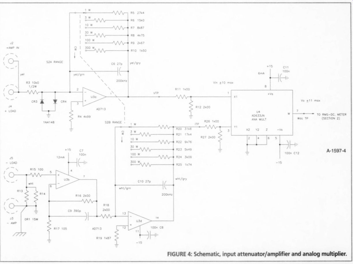
FIGURE 4: Schematic, input attenuator/amplifier and analog multiplier.
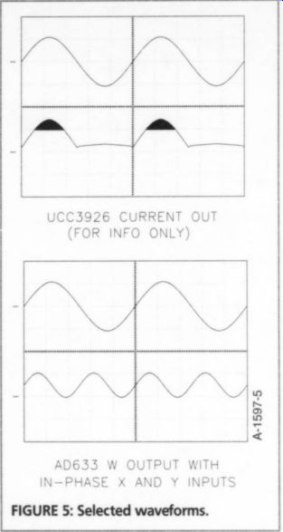
FIGURE 5: Selected waveforms.
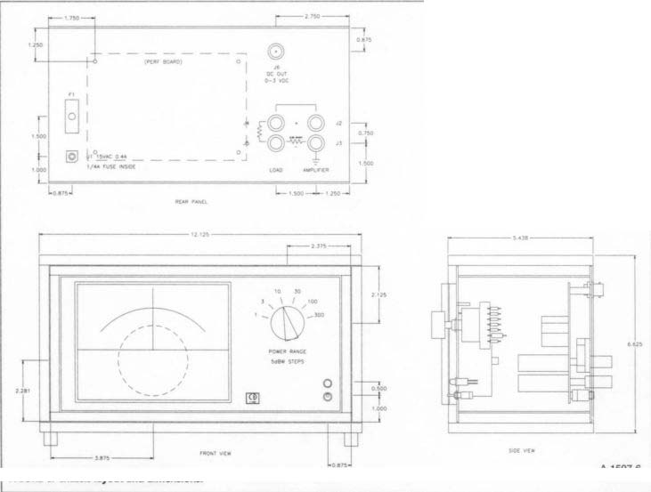
FIGURE 6.
I had great hopes of making this a true power meter, where in-phase voltage and current would result in a directly multiplied output, and voltages and currents 90° out of phase would result in zero output. However, tests with a phase shifting circuit showed that the multiplication method employed by the ADG6G does not differentiate between real and reactive power in this way. The AC component of the W output signal remains constant when the phase angle of current with respect to voltage changes. In stead, phase-angle variations introduce a variable DC component.
Seeking Solutions
When the inputs are sine waves E sin wt, the output is a frequency-doubled sine wave, since
. 2 (Esinax} _ E* -cos2mt) 10 20+
You can eliminate the DC term at the output (1-cos2mt) with an RC network for a fixed-input frequency, but this did not appear to be a practical solution over
G33 the audio band. There may be another solution, but I could not find one in the various application notes for the ADG633, or by experimentation.
When I connected in-phase 1V RMS signals to the X1 and Y1 inputs, the output was a 200mV pk-pk AC signal at twice the input frequency, with a DC component of +100mV (see Fig. 5 again).
When the phase angle was increased to 90°, the DC component disappeared. A phase angle of 180° between the inputs resulted in a DC component of -100mV.
My "solution" was to block the DC component with a series capacitor. Any suggestions by those well-versed in the use of the ADG633 are certainly welcome.
The W output of U4 pin 7 is applied to the RMS-to-DC converter and meter-amplifier section of the meter (Fig. 3). Since the signal from U4 can have a DC component that varies with amplitude and phase angle, as described previously, it is coupled to amplifier U3c via C13 and R28. U3c is used to increase the signal level from U4 and provide a means of calibrating the DC output signal at J6. Pot R30, in conjunction with R29 and R31, sets the DC output voltage at J6 to 3V DC for a full-scale reading on any 0-3 scale range of the meter (3W, 30W, 300W).
With the worst-case input situation (high power on the 1W scale), the output from U3c could be as high as 8.2V peak.
This does not occur at 300W, but at a much lower level, where the input signals to U4 just start to clip. At 300W the in puts to U4 are severely clipped, and the product of the two near-square waves is mostly DC, which is blocked by C13.
Computing the True RMS Value
The signal from U3c is applied to the pin-13 input of U5, a high-precision, wide band AD637 RMS-to-DC converter IC.
This device computes the true root mean-square (RMS) value of any complex AC (or AC plus DC) input waveform, and provides an equivalent DC output voltage. The RMS output at pin 9 is connected to averaging cap C19 at pin 8, and to the denominator input (DEN IN) at pin 6.
The ADG637 contains an internal buffer amplifier, used here as a 3-pole ripple post filter* to reduce ripple, enhance ac curacy, and allow a fast output-settling time. The 3-pole filter components are R32, R33, R34, C14, C15, and C16, and the internal buffer op amp. The 3-pole filter buffer output at U5 pin 14 is applied to J6 via limiting resistor R37. Since R37 is 5k1, any meter connected to J6 should have a high input impedance (1 meg or higher) to ensure accuracy. R35 and R36 zero the DC-offset voltage at the output of U5.
The output of U5 pin 14 is also sent to the meter amplifier, UG, via R39. Since any voltage greater than 3.4V DC will peg the analog meter against its end-stop, possibly causing damage, CR5 and VR1 limit to a maximum of 3.3V the input voltage to U6 pin 3. VR1 (a 2.7V zener) is supplied with about 7mA of current via R38 to keep it above its knee-point current, ensuring a precise clipping point.
CRS is a low-leakage diode, used to avoid any error introduced by reverse-current leakage. R37 and R39 are sized to ensure that current from U5 pin 14 never exceeds its 5-mA maximum output-current capability.
The V,, limit to US is specified as 7V RMS, so you might think it better to place the zener clamp at the input to U5.
The problem is that the input impedance at pin 13 is 6k4 to 9k6L, and I thought that this wide range could affect accuracy if any additional resistance were connected between U3c and U5. The V, input can withstand transients up to the +15 rails, so this compromise won't jeopardize the reliability of the AD637.
The voltage at U6 pin 3 is converted to a meter current for M1 by a V-I converter circuit consisting of U6, Q1, and Q2.
Since there is closed-loop feedback to the inverting input of U6 pin 2, the voltage across R42 and R43 equals the input voltage at U6 pin 3. This is the DC voltage from U5, proportional to the audio amplifier output power. Since the emitter current in Q2 equals the input voltage at UG divided by the sum of R42 and R43, R43 allows you to calibrate the full scale analog meter reading based on the 3V DC signal to J6.
JFET Q1 drives the base of bipolar transistor Q2, so that no error is introduced into R42 and R43 by the addition of base current (I, = I + I). This is necessary because the meter is in the collector of Q2, and the current-determining resistors are in the emitter. The base current for Q2 is the drain current of Q1, which is also in series with the meter, and the gate of Q1 draws no current from the output of U6. CRG will limit the voltage across the meter coil to 0.6V DC if some failure in the meter amplifier circuit causes Q2 to turn completely on.
This is exactly the same meter circuit used in the HP-339A distortion test set, with a different current scaling. 5 R40 calibrates the s-scale meter reading to account for nonlinearities in the meter movement.
Linearity Measurements
I took linearity measurements at every major division on the 0-10 scale with a DC power supply and series 10k resistor.
While M1 is large (6" across the case for the PA3 that I used), it has a -10% error at the low end, a -2% error at mid-scale and a +1% error at full scale. Also, the error and the mechanical zero point varied with the angle of the meter face. It was best when held vertically and worst lying flat, which explains my enclosure.
Since the PA3 meter I used is no longer available, I selected the closest equivalent I could find--the Modutec 3MAS, 0-1mA which is a 3.5" rectangular meter (5% ac curacy with the originally supplied scale). I suggest you take linearity measurements as I did. Since I use two scales 0-10 and 0-3, I can change ranges at approximately the 1/2-scale point to maintain maximum accuracy. I found the error over the top % of the meter was less than +3% after calibration.
The analog multiplier IC (U4) is sensitive to harmonic content. When I used the 60Hz power line as a source (through a 48V AC step-down isolation transformer) to calibrate the high power ranges, I saw a full-scale error of about +3%. The AC power line typically has a 3% THD content; I measured 3.1% with my distortion test set.
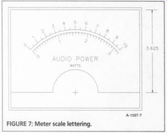
FIGURE 7: Meter scale lettering. Incidentally, I did not apply the 48V AC isolation transformer to an 8-ohm load- that would have required a 300VA transformer. Instead, I used a 1A transformer and a substitute "load" of 800 ohm in series with 5 ohm (1% resistors). This produces the same voltage at the current-sensing jack J5 as the 8-ohm/0R05 ohm combination.
Out of curiosity, I performed some tests with other waveforms. A 3.3W RMS triangle wave produced a reading of 3.8W. A 9.0W RMS signal using square waves produced a reading of only 0.7W.
As mentioned earlier, this is due to the high level of DC content in the W output of the analog multiplier, which is blocked by C13.
Optional Voltmeter
If you connect a suitable high-impedance (1 meg) voltage divider and input-buffer amplifier to the C13 side of Fig. 3, you can make a very nice true-RMS audio voltmeter. You'll need some small attenuator-compensation capacitors for accuracy at high frequencies, as with any high quality piece of test equipment. I leave the research for such a front-end design to you if you're interested.
Construction
Because of the size of the meter, I could not find a suitable enclosure for this project. I built a cabinet out of clear pine and used flat aluminum plates for the front and rear panels (Photo 1). 1 lined the in sides of the wood cabinet with perforated sheet aluminum for shielding, and used four rubber feet on the bottom. You may be more successful in finding a chassis that fits the smaller 3M AS meter included in Table 1. Most meter enclosures have a slanted front for easy viewing, but be aware of the increased errors that I found when my PA3 meter was not vertical.
Figure 6 shows front, rear, and side views of my chassis layout. Figure 7 shows the meter-scale lettering. I copied this to with copier equipped with enlargement/reduction. Since the PA3 meter I used is no longer available, you will need to adjust the copy size to fit the scale of your own meter.
To paste the new meter scale over the old 0-1 scale, you must carefully remove the clear front case from the meter movement after removing any attaching hard ware. Note that the mechanical zero-adjustment mechanism surrounds the sides of the meter needle, so you must lift the front of the case straight up. You could bend or break the fragile meter needle if you apply any force to it. It is a very thin hollow brass tube, flattened at the tip, and easily subject to damage.
FIGURE 7.
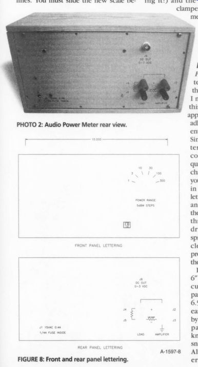
FIGURE 8: Front and rear panel lettering.
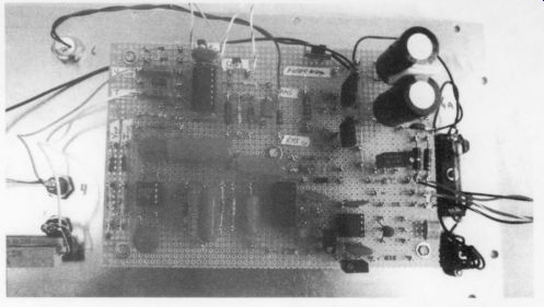
Photo 2

Photo 3
I applied a glue stick to the existing scale and carefully pressed the new scale over it, lining up the old and new zero lines. You must slide the new scale between the meter needle (without touching it!) and the face of the meter. I clamped the back half of the meter in a PanaVise so | would have one less loose part that could move and cause dam age to the needle.
Panel Lettering
Figure 8 shows the lettering designations for the front and rear panels.
I made a full-size copy of this lettering on drafting appliqué film, which is an adhesive-backed transparent plastic (see Table 1).
Since the photocopy lettering is black, a light a color base paint is required, although you can 0 change the letter colors if you use a color cartridge in the copier. Apply the lettered film to the front and back of the unit in the proper locations. Cut through the film at the drilled holes and then spray it with two coats of clear polyurethane for protection. Photo 2 shows the rear of the unit.
I wire-wrapped a 4" x 6" perfboard for the circuitry (Photo 3). (The parts list calls for a 4.5" x 6.5" perfboard. You can easily cut this to 4" x 6" by scoring along the hole 1 pattern with a utility knife on each side, then snapping off the excess.
Alternatively, two suppliers carry 4" x 6" perf A-1597-8 boards:
Parts Express [1-800-338-0531] as p/n 055-352, and All Electronics [1 800-862-5432] as p/n ICPB-46.)
Resistors R5-R10 and R20-R25 are mounted on rotary switch S2.
Double-check the orientation of the polarized components. I used sockets for the DIP ICs, and checked the power-supply voltages at the IC pins before installing them.
Figure 9 shows the perfboard parts placement I used, the outlines for the semiconductors, and the wiring to parts located off the circuit boards. I used an insulating bushing for J1 and J6 to avoid ground loops. Make sure you connect the ground (ring) side of J1 to circuit ground. I installed a 35" ring terminal between J3 and the bare aluminum rear panel for use as the chassis ground point.
I also bent small aluminum tabs to make ground connections between the front and rear panels and the perforated shield that lines the enclosure.
Install all the mechanical parts on the front and rear panels, and wire the perf board to its rear-panel components, using twisted wires from the board to J1 and J6. Install the front panel, then open the rear panel with the perfboard in a position where you can easily replace the fuse. Finish the wiring from the perf board to the front-panel switches, the LED, and the meter. Use twisted wires from the board to S1 and the LED.
Photo 4 shows an interior view of the Audio Power Meter, with the rear panel open to show how the PCB is attached.
Photo 3
Calibrating the Audio Power Meter
* Set the mechanical meter to zero with no power applied to J1 (and no test amplifier connected, of course);
* Apply power and allow the unit to warm up for 15 minutes;
Adjust R36 for 0V DC at the output to J6;
Apply an accurate, undistorted 3W audio signal to the input (J2-J5) at 1kHz. The amplifier load can be either 4 or 8-ohm. You can calculate the output power by
P = E2/R (you must add the internal 0R05L to your load resistance R);
Select the 3W range with S2. Adjust R30 for a 3V DC output signal at J6.
The meter connected to J6 should have a high input impedance (1 meg or higher) since J6 has a series output resistance of 5k1;
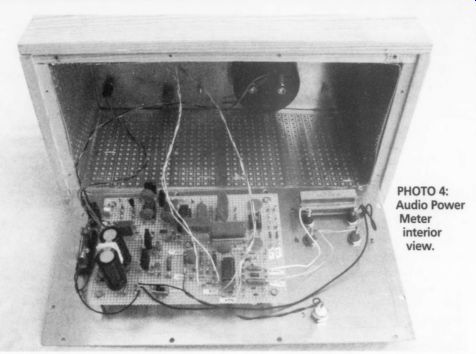
PHOTO 4: Audio Power Meter interior view.
Adjust R43 for a reading of "3" on the 0-3 meter scale. This is full-scale on the lower scale;
Reduce the audio amplifier input to 1W, and adjust R40 for a reading of "1" on the 0-3 meter scale. This is 1/2-scale on the lower scale;
The adjustments of R40 and R43 inter act somewhat, so repeat the calibration for R43 and R41 as described previously until the best accuracy for each reading is achieved. Adjust R43 last, since accuracy is more important at the high end of the scale;
*With the audio amplifier input at 1W, select the 1W range with S2. Check that the meter reads 10 on the 0-10 scale;
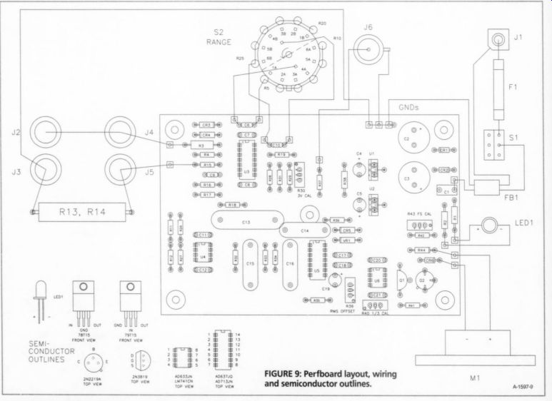
FIGURE 9: Perfboard layout, wiring and semiconductor outlines.
Slowly increase the audio input power on the 1W scale until the voltage at J6 exceeds 3.5V DC. Make sure the meter needle stops just before the "pegged" position. This checks operation of the meter-protection clamp;
Return S2 to the 3W range and maintain a 3W reading on the 0-3 scale.
Change the input frequency to the amplifier to 20Hz, then to 20kHz. The meter reading should remain greater than 2.85W (-0.22dBw, or 5%):
You can now apply increased levels of power and check the higher meter ranges. Do not exceed the 1% THD clipping point of your power amplifier.
If you frequently test tube amplifiers, you may choose to calibrate the meter at the 3% THD clipping point. You could also add a switch with calibrations at 1% and 3%, as you can see in Photo 1, although I have not yet made it functional.
References
1. UCC3926 Integrated Current Sensor data sheet, www.unitrode.com
2. "+20A Current Monitor," Elektor Electronics, Issue 7-8/99, p. 40.
3. D. Lancaster, "Some New Current Sensors," Electronics Now, July 1999, Fig. 4, p. 90.
4. Analog Devices Applications Reference Manual, 1993, Applications Note AN-268, "RMS-to-DC Converters Ease Measurement Tasks," pg. 17-14, Fig. 23. Additional application information for the AD633 and ADG637 is available in the Analog Devices Special Linear Reference Manual, 1992.
5. The same circuit appears in the 1986 National Semi conductor Applications Handbook, AN-20, Fig. 17, p. 25, "Precision Current Sink."
Sources:
Digi-Key 701 Brooks Ave. South Thief River Falls, MN 56701-0677 1-800-344-4539 digikey.com
Mouser Electronics 958 N. Main Mansfield, TX 76063-4827 1-800-346-6873
Newark Electronics 4801 N. Ravenswood Ave Chicago, IL 60640-4496 1-800-463-9275 newark.com
Old Colony Sound Lab PO Box 876 Peterborough, NH 03458-0876 603-924-6371 audioXpress .com
Radio Shack Local Stores, or Radio Shack Unlimited (RSU) 1-800-THE-SHACK tandy.com
Also see: