Several years--and a lot of hard work--later, here is a new version of the popular super regulators first published in AE.
Mark K's initial letter (see p-17), which I received in very late 1998, turned out to keep us busy with investigations for a few months. From those experiences emerged the improved positive and negative regulator circuits described here.
For reference purposes, we will refer indirectly to the original schematics associated with the Old Colony PCBD-3A/B printed circuit boards (PCBs) as they were published in Jan Didden's "Regulators For High-Performance Audio, Part 3" (TAA 3/95, p. 20). Note that one of these PCB sets implements paired * regulators.
To retain full compatibility with the art work of the 1995 card design, the changes described here modify no PCB tracks and require no additional holes.
As shown here, we have two new, complete regulator schematics, both consistent with the original PCBs. Note that these two new figures (Figs. 1 and 2) cover both the original form as well as the new modifications described here. Figure 1 is the positive regulator form, and Fig. 2 is the negative. These figures correspond respectively to the original positive and negative regulator circuits, Fig. 2 and Fig. 3 in the previously cited article.
Taking the easiest problem category first, Mark Kovach's range of regulated voltages can be considered normal. With regard to Fig. 1, considering D1's LM329 reference tolerance of 5%, and adding the 2% scaling R5/R3 resistor tolerances, the output can be roughly 2 x 6.9V +7%, or 12.83-14.76V. That's actually a wider range than Mark quoted, so it sounds as though he had a few very close LM329s, possibly from the same batch. Of course, these absolute DC voltage variations don't affect sound directly, as noted by Jan Didden in the 1995 article (p. 21).
Startup Problems and Cures
More serious is the issue of regulator start up. For some of Mark's eight regulator B cards, we resolved the startup problems easily, while incorporating some simple design improvements. For others, the solution was more subtle, yet still simple.
Referring to Fig. 1 again, consider the original form of the circuit, that is, using the dotted-line components. Then, visualize the effect of the voltage drop across the originally used 1N4148 diode D8 upon startup. If the opamp goes LO initially (i.e., towards the negative rail, or ground), the 0.6V drop across D8 will essentially be cancelled by Q1's Vg, which makes voltage V,, seen at PCB terminals T2/T9 nominally equal to the op amp LO state saturation voltage.
Note that terminals T2/T9 are Jumpered external to the PCB in normal operation, as are T10/T20. The LO state saturation voltage for the AD797 is about 2V. So, if for any reason X1 gets stuck in the LO state, V+ will rest around 2V, essentially what Mark re ported. This is by definition a false-start condition.
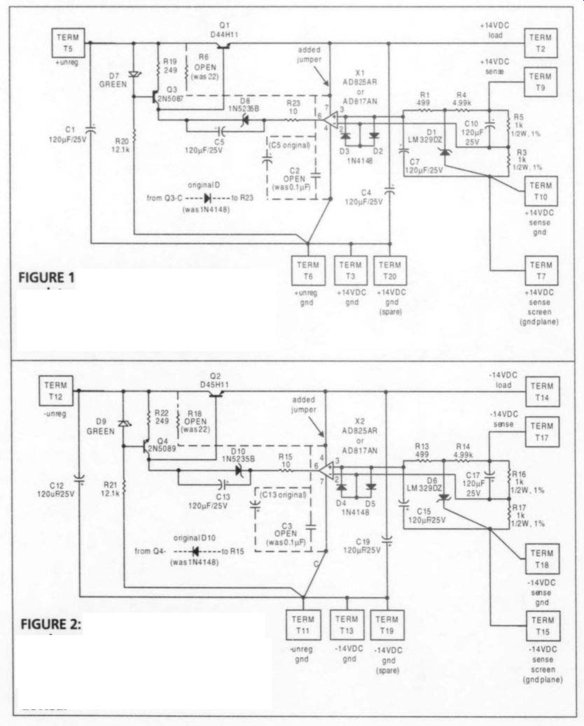
FIGURE 1: Improved positive output regulator circuit, incorporating op-amp supply bootstrapping, enhanced startup, and new op amp. Note-original positive regulator connections shown dotted.
FIGURE 2: Improved negative output regulator circuit, incorporating op-amp supply bootstrapping, enhanced start up, and new op amp. Note-original negative regulator connections shown dotted.
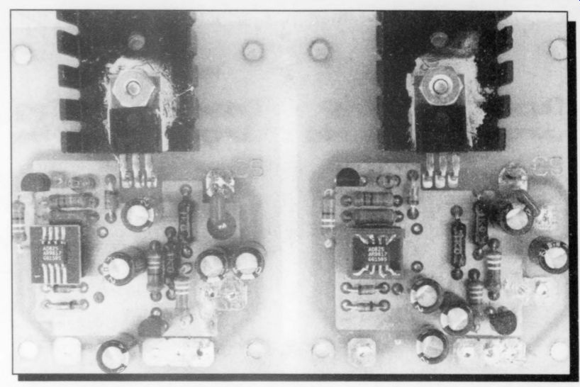
PHOTO 1
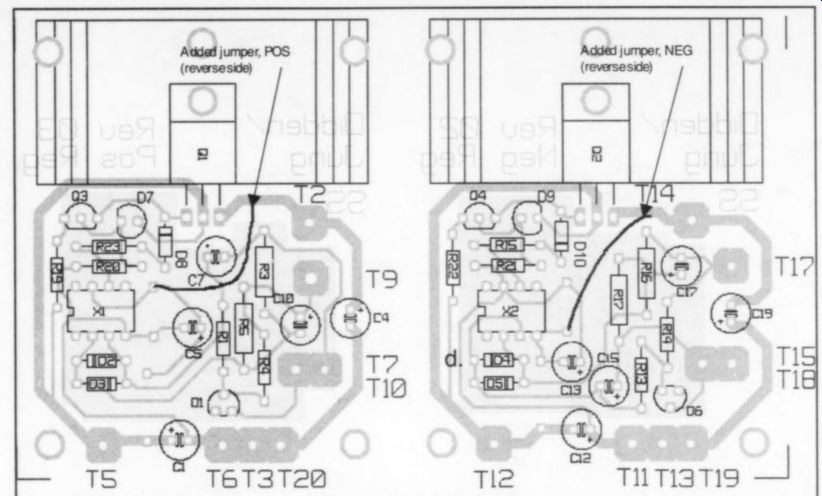
FIGURE 3: Stuffing guide for the improved positive/negative regulator board. For reference, C5 and C13 are shown here in original locations.
Mark and I exchanged a number of e-mails and phone calls in troubleshooting his regulators remotely, without full success. For some time I had been working on upgrades to this circuit-some simple, others more complex. The most direct of these is a simple one-for-one component substitution for diode D8 (or D10) (Photo 1), replacing Fig. 1's D8 IN4148 (D10 in Fig. 2) with a 6.8V zener. The 500mW 1N5235B is both mechanically and electrically suitable.
In doing this step, however, it is critical to note that a zener installed for D8 (D10) must be polarized exactly opposite to the original 1N4148, so as to operate in reverse-breakdown mode. That is, the diode is installed with the cathode to wards Q3-C in Fig. 1 (or anode to Q4-C in Fig. 2), i.e., just as shown in the respective figures. For reference, the original 1N4148s are also shown dotted. Note also that shunt capacitors are added, C5 in Fig. 1, C13 in Fig. 2. These are further discussed later in this article.
As far back as August 1995, Jan Didden and I explored operation of such bias networks for startup aid within new regulator forms operating the op-amp supply from the regulator output, i.e., bootstrapped. Bootstrapping here refers to operation with the op-amp rail voltage derived entirely from the main output (as opposed to operation from the raw DC supply via R6, as in the original circuit). Bootstrapping has the highly desirable advantage of improving the line rejection of a so-modified regulator to well beyond that of a comparable, but conventionally powered version.
To implement bootstrapping, Jan had first tried a couple of forward-biased LEDs for D8, while I suggested a 6.8V zener as preferable. My testing found that the higher-voltage zener diode biasing was absolutely required for a boot strapped version of the regulator; otherwise, it wouldn't start reliably. This should be readily apparent, since the op amp can't operate dependably until it has sufficient supply voltage. Thus to implement a reliable bootstrapped regulator, the breakdown voltage of D8 (or D10) must allow the circuit sufficient voltage to start unfailingly.
Jan Didden had tried the bootstrap mode of operation first; then I tried it later on, and also published a boot strapped form of the original 14V regulator in "Regulator Excels In Noise and Line Rejection," EDN, Jan. 2, 1997. A 5V form of the bootstrapped regulator was also described in Walt's Tools and Tips, "Low-Noise Power for Analog Circuits," Electronic Design Analog Applications Issue, June 23, 1997.
However, it is worth noting that at neither that time nor since have I ever personally seen a startup problem with the original 1995 circuit, with all components operating properly. I saw the false start conditions only when the circuit was modified for the bootstrapping. More details on this later.
To summarize, the primary goal of the additional bias voltage is to provide enough initial output voltage so that the op amp always has a sufficient supply of operating voltage. With D8 chosen correctly, this also forces reference diode D1 to break down. Since the LO state output saturation of the op amp is ~2V, choosing a voltage for D8 nominally equal to the reference ensures this.
In the example here, 6.8V + 2V - 0.6V provides about an 8.2V initial output.
Note that in the original positive (or negative) regulator circuit(s), changing only D8 (or D10) to a 6.8V zener diode provides the additional bias, and this change can be implemented by itself with no side effects.
Mark first implemented the 1-for-1 zener-for-1N4148 replacements in the D8 (D10) locations of his regulators, and this fixed four of the eight circuits. Further troubleshooting with the others revealed some bad parts, but a couple still stubbornly refused to start.
To get to the bottom of the problem, I agreed to examine these for him. Our agreement was that I would test and fix the two problem card sets, and at the same time upgrade one set of the + output paired regulator card sets with some other modifications I had been testing, including the supply bootstrap operating mode. He would then complete these additional upgrades on the remaining positive/negative set when I returned the cards, as well as his remaining sets.
To briefly summarize tests on these two-card positive/negative pairs, in the first set the positive output (POS) card wouldn't start at all, which was traced to a bad resistor and/or solder contact around R4. Replacing R4 fixed the start up problem. The NEG regulator of the set started OK, but the output wandered several mV. This anomalous variation was traced to a flaky LM329 (D6), where a replacement fixed things.

PHOTO 2: Bottom PCB-side view of the improved regulators, again modified as per Figs. 1 and 2. Note new V, insulated bus wire jumpers, plus newly located C5 in the positive regulator (right), and C13 in the negative regulator (left). Be sure to orient these caps with the (+) lead towards the D8 (or D10)cathode.
-------------
TABLE 1: PARTS LIST
Miscellaneous items:
Quantity (2) TO-220 low-profile PCB-style heatsink, 15.6°C/W (Digi-Key HS112-ND or equivalent for PCB mounting); quantity (1) Old Colony PCBD-3A/B circuit-board set, as required; mounting hardware; 18AWG hookup wire, and so on.
------------------
On the second + set of PCBs, I also found a startup problem with the POS version. This was traced to an apparently bad solder connection around the same resistor, R4. I re-soldered everything around these components and lifted the body of the resistor up away from the ground plane, and it then fired up OK.
A caveat here for anyone working with cards like these, with a ground plane beneath components: There may be some potential for any exposed component leads to touch the ground plane and short out, so be careful! As one example, this is possible with an exposed end cap on the Vishay Roeder stein MK-3 2W metal film resistors Mark used. While there is nothing generally wrong with using these resistors in all locations (they are good), the caveat I note is to be especially careful that the end caps of metal films never lie directly on the ground plane.
To summarize the diagnosis of the non-starting regulators, the tip-off symptom was that there was little or no voltage developed across D1. Specifically, this voltage measured only about 10mV, where it should normally be 6.9V! With a broken conduction path through R4, there is no way for the op amp to properly sense the inputs, and thus the output stayed stuck in a LO state. This persisted until R4 was repaired, whereupon the circuit then started OK. So, as with any quality audio circuit, careful assembly work is required for correct results.
Additional Regulator Enhancements
Several other regulator enhancements were added to the first pair of Mark's cards as I tested them. He subsequently replicated these same changes on the second set of cards, plus his other two sets (four sets total, eight regulators in all).
These changes were referenced in his second letter (p.17), along with his reaction to their performance in his system.
1) Change of current source resistor:
As part of an overall upgrade, the value of the current defining resistor in the current source is raised. This step eases the current and power loading of the op amp by lowering the current from 10mA to 5mA.
With a minimum gain of 40 in the pass transistor, this still allows an output drive of at least 200mA from the circuit.
If you would like to verify this for yourself, test the regulators with a DC load of 100Q, which validates it for more than 140mA. Then, in your final circuit, you can simulate a net 100mA load by using a dummy resistor to bring the load up to 100mA (assuming that the active stages will draw less current).
a) (POS): Change the value of R19 to 249 ohm.
b) (NEG): Change the value of R22 to 249ohm.
I recommend adding a dummy resistor calculated as:
P- = 14/(0.1 - x),
where x is the current drain of your pre amp circuitry, in amperes. For example, if your preamp draws 0.025A, an R of 186 ohm is OK. The nearest standard value is fine, and make it a 5W type to be safe. Do this for both positive and negative supplies.
2) Bootstrap op-amp supply lines:
To implement the bootstrap supply mode for the op amp, the original connection to the unregulated input via a 22 ohm) resistor is opened, and the opamp rail pin is connected directly to the V,, line, between the pass transistors and the output pad. The film bypass capacitor near the op amp is also removed.
A special note is applicable to the use of bootstrapping mode: Bootstrapping must be done along with the 6.8V zener update described previously. It won't work with the original 1N4148 used for D8 or D10.
Note that a revised stuffing guide appropriate to the schematics of Figs. 7 and 2 is shown in Fig. 3. Be aware that it reflects all subsequently described changes, i.e. steps 2a, 2b, and 3.
a) (POS): To enable bootstrapping of the op-amp supply line in a positive regulator, simply remove (or do not install if building new) R6 (22 ohm) and C2 (0.1uF) and jumper the V+ line from X1 pin 7 to the Vr = 14V pad TERM T2.
Place this jumper on the back (trace) side of the board as shown in Fig. 3 and Photo 2, sol der carefully at both ends, and use sleeving over the lead. I recommend Teflon sleeving if you have it, but any good-quality insulation will work. If you execute this change, verify that D8 is a IN5235B, polarized as shown in Fig. 1 and Fig. 3.
b) (NEG): To enable bootstrapping for a negative regulator, remove (or do not install if building new) R18 (220) and C3 (100nF) and jumper the V- line from X2 pin 4 to the Vg = -14V pad TERM T14. Again, place this jumper on the track side of the PCB as shown in Fig. 3 and Photo 2, solder carefully, and use sleeving. If you execute this change, verify that D10 is a IN5235B, polarized as shown in Fig. 2 and Fig. 3.
3) Op-amp changes:
Related to the Figs. 1 and 2 regulators, it has been verified that they are stable with the AD797 and the AD817 op amps, as well as the AD825 (see later). However, it is now recommended that the op amp in both regulators be changed to a new type-ei her an AD825 or an AD817. Since the PCB accepts an 8-pin DIP device, the AD817AN can drop directly into the circuit in place of the AD797, with the only associated change being the inclusion of the back-to-back 1N4148 protection diodes (D2-D3 of Fig. 1 and D4-D5 n Fig. 2).
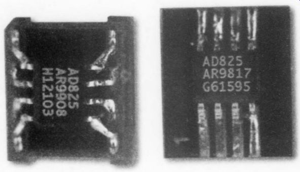
PHOTO 4: Close-up view of one pre-reg, with clip-on heatsink attached.
PHOTO 3: Close-up view of three op-amp configurations. At left is an AD817 header module, with the optional RC network, as per Fig. 5(a). In the middle is an AD825 mounted on an 8-pin DIP header, and at the right is another AD825 mounted on the SOIC-DIP adapter. With the use of the 8-pin DIP header, all pins of the AD825 need not be soldered, since 1, 5, and 8 aren't connected. They can be (carefully) snipped off prior to soldering the others.
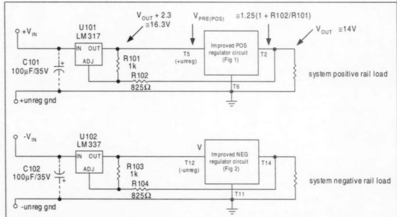
FIGURE 4: Higher performance option using U101 (POS) and U102 (NEG) off-card,
floating IC pre-regulators.
Note that since similar protection diodes are internal to the AD797, they aren't necessary in that unique case. But, they are appropriate with the AD817 (or any other unprotected-input op amp).
The AD825 should not require protection for normal +/- 15V level supplies.
The AD825 op amp, available only in an 8-pin SOIC package, will require the use of some sort of SOIC-to-DIP adapter to match the PCB footprint of Fig. 1 or 2.
Two methods have been used to accomplish this. The more expensive route is to use a true 8-pin SOIC-to-DIP adapter, such as those by Aries. As an alternative,
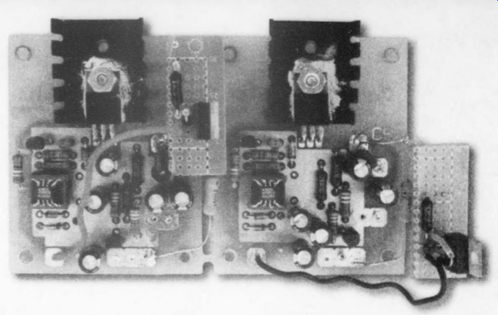
PHOTO 5: Top PCB-side view of improved regulators, modified as per Figs. 7
and 2, with AD825s on headers. Figure 4 pre-regs are included, to the right
side of the positive and negative PCB sections, respectively, mounted on proto
board sections. The pre-regs' clip-on heatsinks were removed for this photo.
the tiny SOIC IC can be soldered directly to an 8-pin DIP header (also made by Aries), which is then soldered in place as a conventional 8-pin IC.
While the parts list (Table 1) includes both adapters, frankly, I prefer the less expensive header solution. Implementing it is tedious and does re quire close, careful work in alignment and soldering.
If you opt for this, it helps to snip off the unused AD825 pins (1, 5, and 8) and to pre-align the 0.1" centered header pins. Bend them slightly inward to form a "shelf" matching the SOIC pins. Then (taking care that no solder wicks between adjacent SOIC pins 2-3, 3-4, and 6-7) solder the IC pins 2, 3, 4, 6, and 7 to the like numbers of the header. Be fore installing the finished IC along with header or adapter onto the PCB, carefully inspect the assembly for shorts and solid solder connections. Photo 3 shows header and adapter modules, ready for PCB mounting. Photo 4 is a very close up view.
The use of the AD797 op amp in these regulators has not been without some problems, mainly associated with stability. This was noted in Gary Galo's "Regulators For High Performance Audio, Part 4" (TAA 4/95) and also in Jan Didden's "So It Oscillates-Now What?" sidebar within that same article.
Jan's dissatisfaction concerning the AD797 has been consistent since then, and in fairness to him, it should be noted that he has desired to change from that device from the outset. Until as recently as late 1998, I had resisted this, and was still using the AD797 in various regulators. I did need to deal with some cases of stability along the way, but none in which careful attention to bypassing, decoupling, and so on couldn't be made to prevail, and so yield net overall regulator stability.
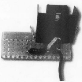
PHOTO 6: Very close-up view of AD 825s mounted on an 8-pin DIP header (left) and SOIC-DIP adapter (right). Take special care to note the orientation of pins 1-4 of the SOIC package on the header (at left side) and the SOIC-DIP adapter (at bottom side). These pins are denoted by the sloping side on the SOIC package.
That lasted until the end of 1998, when I encountered a situation where use of the AD797 gave rise to spurious responses. This was within a 12V version of the regulator used in a synthesized FM tuner. What, you ask, is so different about such an environment, so as to make it unfriendly to a low-noise device like the AD797?
Simply put, it was the high levels of 100MHz TTL clock noise associated with the physical grounding scheme of this design.
Very high levels of RF noise were present (note that "high" here need only be a few mV in amplitude, considering the normal microvolt-level error signals of a high gain-bandwidth device like the AD797). This level of high-frequency noise is sufficient to push a low-noise bipolar front-end device into a nonlinear input operating range, where it can then detect spurious signals mixed with real audio-frequency error signals.
Although the AD797 didn't oscillate outright in this setup, it simply wasn't as linear an error amplifier as might be desired. As for examples of devices less susceptible to front-end nonlinearity, in general this would include low transconductance input-stage parts, such as FET input devices, or highly degenerated bipolar input-stage units.
----------------
JUST HOW DOES IT START?
There has been considerable curiosity on the part of some correspondents as to just how the original regulator starts up in a correct state. This is worth a side discussion, because there are multiple mechanisms inherent to both the original and new circuits that provide this useful feature.
First, it should be noted that in the default power-on condition of Fig. 7 or 2, current source Q3 (or Q4) will always tend to turn on the pass device. Then, for normal operation, the op amp shunts current away from the pass device and establishes the precise operating conditions for a given design. So the current source is the first level of fundamental operation that will always try to bring up the output.
Second, there are several more involved levels of op-amp operation as it powers up. The answers to this lie in the details of the startup bias networks and how they relate dynamically to op-amp input voltage sensing. Regarding Fig. 1 (again), in the original configuration with the 1N4148 diode, the diode forward voltage and Vy; of Q1 essentially cancel, so the X1 output voltage is equal to the overall output voltage (within a hundred milli volts or 50).
For all output conditions, note that the X1-Q1 output voltage V,, appears at the junction of R4 and R5. And, for the op amps typically used (i.e., the AD797 and others), the lowest possible V,,- voltage Vouraoy
Will be about 2V above the op amp's negative rail voltage. Since all these regulator circuits have the opamp common rail grounded as shown, V1, is then simply 2V.
We define phase 1 of regulator operation as the time interval immediately after input voltage un is applied. In the first few milliseconds of this phase, the X1 (+) input sees the voltage across C7, which initially will be very close to ground. This essentially zero voltage, combined with a much higher, close to V1, potential at X1 (), causes the opamp to act as a comparator within this phase (i.e., no overall feedback-loop closure, and an output stuck at one rail limit, negative).
The relative sign of the two inputs forces X1 to remain at Vip, for an initial period of time. At the same time, however, the network R4-R1 sees the ~2V Vout ao) voltage, and thus C7 begins to charge towards V,,.;.
As C7 charges, the X1 (+) input eventually reaches the X1 (-) potential.
At the point where the two X1 inputs first enter their linear range, the op amp becomes active and begins to control V_out.
This is phase 2 of regulator operation, with X1 now operating in a linear mode (as opposed to phase 1, with X1 simply a comparator). In phase 2, the circuit enters a controlled, positive-feedback dominated timing sequence, with V, ramping upward. In this interval, Vg rises towards the ultimate V,. At an intermediate point, when V.. reaches 6.9V and reference diode D1 breaks down, the circuit then enters into its final operational sequence, phase 3.
In phase 3, with D1 operating at 6.9V, C7 settles to a final voltage value of 6.9V, overall negative feedback dominates, and V_out settles out to the design value of 6.9 x (1 = R5/R3) volts. With the values in the circuit, this entire sequence takes about two seconds, with V,,. settling to a nominal 13.8V.
To provide some data on this operation, I set up a couple of tests to illustrate this sequence and to test the general robustness of the circuit. I used the original TAA 3/95 Fig. 2 circuit, with the AD797 and the 1N4148 diode for D8, and a switched ON/OFF mode 18V input, interrupted on a two second ON/OFF period.
To see more easily the timing wave forms, I reduced C7 and C10 to 10pF, which allowed the ~14V output level to be reached in about 160ms. I ran this test most of a day, that is, more than 10,000 ON/OFF cycles, without evidence of a false start. This would probably serve as more than minimum simulation for typical equipment lifetime tests-allowing for one ON/OFF regulator cycle per day, it corresponds to over 27 years of operation.
It is also well worth noting that the regulator configuration used tends to be self correcting as it goes about following the three-phase sequence just described. This is because of the two separate feedback paths, one of which dynamically takes precedence, depending upon the relative output voltage.
The positive feedback path is via R4-D1 R1, and it has essentially 100% feedback when Vp is < Vege, and zero feedback when D1 is regulating and Vy, is >Vee.
The negative path is via R5 and R3, and it is subject to the division ratio of the values chosen. This dual-mode operation is what gives the circuit its property of self correction, since the positive-feedback path predominates during phase 2 of startup, and then the negative path takes over once D1 breaks down, removing the positive feedback (phase 3).
However, given all of this, there may also be a soft false start, a condition which Mark's original regulators must have been experiencing. Note that he reported being able simply to probe the circuit and start the regulator into a correct output state.
An unstable connection, perhaps? Of course, the common-mode range of the op amp comes into play here. When and if this is violated, the output won't be of the proper sense, and can't be coaxed into it. This constitutes a hard false start.
This condition is what was found with the second POS regulator, where the measured input was only 10mV. This can be fixed only by correcting the offending component(s). And, in fact, this is just what fixed Mark Kovach's regulators.
Although the above sequence of op amp power-up operation is described in a context of the original circuit, it also holds in principle with the use of a zener for D8 (or D10). The higher startup voltage provides an even more forceful startup progression.
-WJ
--------------------
For more on the theory behind this type of nonlinearity, see my discussions in Walt's Tools and Tips, "Op Amp Audio: Realizing High Performance Bandwidth Limitations," Electronic Design, December 1, 1998.
It turns out that a high-slew-rate bipolar input device such as the AD817 is much more immune to RF detection, albeit at the expense of some noise performance. Similar comments also apply to high-speed JFET input devices like the ADS825. For both lab results as well as theoretical discussions of the RF detection phenomenon, see Adolfo Garcia's "Input Stage RFI Rectification Sensitivity" in System Applications Guide, Walt Kester, Ed., Analog Devices Inc., 1993, pp. 1-37 through 1-55.
At this point, I am of the opinion that very high gain-bandwidth, low-noise amplifiers such as the AD797 need to be very carefully applied in audio stage regulators. Speaking more generally, this includes not only the AD797, but also many other un-degenerated bipolar input-stage parts. In fact, this type of amplifier may not be an optimum choice at all. Although bench-measurement results with the AD797 are superior in many regards, they simply don't tell the entire story, especially when high-speed, high-level clock signals are factored into the picture.
As a general qualification, I would now say that all high-performance audio regulators should be carefully evaluated for the best amplifier suitable. It is important to note that, because of the RFI sensitivity issues previously described, this choice may not necessarily include such steadfast favorites as the 5534 and 5532 families, as well as many other un degenerated bipolar input-stage devices.
To summarize the op-amp selection story, what it now comes down to is a choice of the AD817 or the AD825 in place of the AD797. With linear front ends and very high speed, the AD817 and AD825 offer good RF immunity.
In the FM tuner tests, I had first tried the AD817 and AD825, and both worked well. However, I had been reluctant to generally recommend the small-outline integrated circuit (SOIC)-only packaged ADS825 used in the Fig. 1 and 2 regulators, simply because the PCB pattern uses an 8-pin DIP footprint. My original thinking was that it would be an unpleasant challenge and a big hassle for folks to wire up an adapter just to be able to plug the AD825 SOIC IC into the card.
But I was soon advised otherwise by Mark Kovach and his audiophile test group, who ran some A/B tests of the ADB817 versus the AD825, as alternated within his modified regulators (as per Figs. 1 and 2). Most of his listeners preferred the AD825 in terms of the resulting sound from Mark's system. While this preference is one I share, it is likely more useful for readers to know that several additional people with no interest in one op amp versus another had preferred the JFET input amplifier. Nevertheless, readers building the new circuit can also try both op amps for them-[…]
-------------
AN OPTION FOR EXTRA STABILITY AND/OR RFI PREVENTION
As a footnote to the stability discussions in the main text, and to further address the issue of regulator stability, I present here a special compensation technique for the regulator op amp. It is intended for extreme cases of instability, and then only if necessary.
One example would be a regulator circuit that must directly drive small-value, high-Q bypass caps, i.e., in the 0.01-0.1pF range. Although this type of bypass isn't recommended, some folks still insist on doing it (if my troubleshooting e-mails mean anything). Another example could be a regulator that must be used within a strong RF field. The compensation method consists of two RC networks that make up a composite compensation/filter assembly, as shown in Figs. 5a and 5b.
Because of the fact that in Figs. 7 and 2 the common op-amp supply pin differs between the negative and positive regulators, there are two versions shown for the RC compensation networks. This subtle differentiation is simply to allow the best possible ground path for C1. The 5a version suits positive regulators, while the 5b version suits the negative. V The intent is that, in either case, a completed subassembly of 5a or 5b is used as a ' drop-in replacement i for an op amp at locations "X1" or "X2," either within Fig. 1 or Fig. 2. The assembly can be built on an 8 pin DIP header, as Pos Input header assembly shown at the left in Photo 3.
Note that this RC network inserts a 499 ohm resistor in series with each op-amp input and adds high-frequency filtering via the 100pF caps, which are returned to a low impedance point. If present, this network reduces the op amp's effective gain to unity above about 3MHz.
While it has little effect on operation in the audio range, it does have a very useful effect on RF signals, by keeping them away from the op-amp inputs. It also has the nice attribute of electrically removing the pass transistor from the feedback path above 3MHz, thus providing greater isolation from reactive loads.
Since the use of this circuit requires breaking the op-amp input path for R1-R2, it isn't compatible with the Old Colony PCBs. If necessary, it can be retro fitted to an 8-pin header, along with a piggyback opamp and the RC components, to stabilize an op amp even further.
For example, the AD817 works fine with this network added, which does help high-frequency stability. With this compensation network in place on one of Mark Kovach’s PCBs, I was able to apply high-Q capacitive loads to the output of the AD817 + regulators without oscillations. But, alas, this trick definitely does not work with the AD797. It is recommended only for those op amps that are AC stable with 100% capacitive feedback at high frequencies.
On the other hand, for normal cases, there doesn't seem to be any fundamental necessity to use these RC networks within the new regulator circuits when using either the AD825 or the AD817 op amps.
Obviously, that simplifies things consider ably, and most readers can safely just ignore this option. Indeed, the Fig. 5 RC compensation networks should be considered as an option for use in stubborn applications. All of the other changes de scribed can be implemented without it.
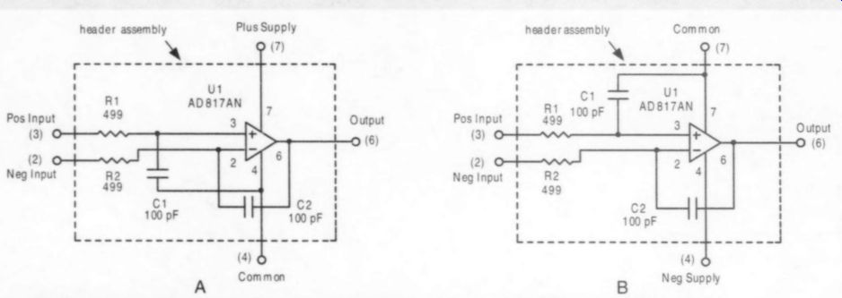
FIGURE 5: Optional RC compensation networks for use in X1, X2 locations within positive and negative regulators.
------------------
Now, Even More Options
Some time after we all thought things were done on the "Improved Regulator" project, two additional developments came along that had a further impact. As mentioned earlier, I had been working on other, more extensive regulators, offering several other circuit enhancements. But, unfortunately, these more complex changes were simply not feasible within the context of the original PCB set, since they required additional components. So most of these changes simply hadn't been considered for this project, due to those basic physical limits.
Nevertheless, audiophile mania being what it is, I guess it was inevitable that someone would try some portions of the new circuits. In fact, this was done by both Rick Miller and Mark Kovach, who added other modifications using a preregulator (pre-reg) stage. Rick modified a 5V regulator in his CD player, using the pre-reg shown in Fig. 4. With the same circuit, Mark modified his system's +/- 14V regulators a la Figs. 1 and 2.
Of course, this optional modification to the regulators of Figs. 1 and 2 is not an outright mod to those circuits i; rather, it is an add-on type of mod that works as follows.
One of the limitations of the Fig. 7 and 2 circuits is the dynamic stability of the current sources (Q3 and Q4). While this situation is difficult to address totally by simple component changes to the card's circuits, one direct way of impacting it positively is just to add an external pre reg. Accordingly, this specific improvement is one of the main features of the Fig. 4 circuit.
When operated in conjunction with either Fig. 1 or 2, the pre-reg stabilizes the input voltage to the card, thereby decreasing the sensitivity of the current sources to unregulated input voltage changes. It also has some more subtle and useful side benefits. By choosing a relatively low output voltage (2.3V) from the pre-reg, the power dissipation of the pass devices is much decreased.
If, for example, +V,, were 10V above V_out regulator without the pre-reg would dissipate 1W with a 100mA load.
With the pre-reg, this dissipation reduces to 0.23W. The bulk of the power being dissipated is transferred to the external IC regulators U101 or U102, leaving the main regulator of Fig. 7 or 2 to do fine control.
------------------
LETTERS FROM MARK KOVACH TO AE
Original Nov. 1998 letter:
Recently I built eight Didden/Jung regulators (four positive and four negative) as described in The Audio Amateur 3/95.
Used with a front-end supply similar to one described by Rick Miller (TAA 4/95) my preamp/crossover has never sounded better. But I have a few questions regarding some kinks I have encountered.
I am using the Panasonic green LED, AD797, and the 10 ohm/.01pF R/C anti-oscillating network. When working, all positive regulators give me 14.06V under load conditions, as also does one of the negative regs (-14.06). However, the remaining three negative regs give me-13.87V.
Did I do something wrong? Why would three negative regs give me -13.87V while the others, including one negative, give me +14.06V? Has anyone else had a similar experience? Sometimes on power up, one positive and one negative reg does not charge to full voltage, remaining at about <2V.
These are not a pair; rather, each is on a board coupled to another working regulator. After lightly touching several components (usually caps) the reg charges up.
The odd thing is that it isn't the same component every time.
I have soldered about a million connections in my life and haven't had a problem with that in over 20 years. All components are new, recently purchased from Digi-Key or Allied. The boards are recently purchased from Old Colony (however, they must be a new run, since I had to wait about eight weeks for delivery).
Has anyone had a similar problem? Is there a component change that I may have missed in a later issue of TAA? If not, can you point me in a direction that may help me locate the problem?
March 1999 e-mail:
What has transpired as a result of my previous letter is well worth mentioning and printing, since it can greatly upgrade the quality of the systems of many AE readers.
In January 1999, Walt Jung contacted me via e-mail regarding the problem I was having with some of the regulators. During the next three months, we corresponded on a regular basis, and Walt came up with a simple fix for my problem, which I installed and tested. It involves changing one component.
As you can see by my first letter, the regulators are a fantastic improvement, and-without any startup problems-are a welcome addition to my system. But we didn't stop there. Walt resurrected a boot strapped version of the regulator and adapted it to the original cards. It involves a little more work, including some PCB jumpers and a few component changes, but I easily adapted it to the cards. There is also an optional R/C network that you can attach to the IC for added stability.
I have tested this version of the regulator in my system for more than a month and can say without hesitation that the increased definition and wider soundstage are worth all the time Walt and I spent to get to this point.
------------------
The expression for the pre-reg’s floating output voltage, Vppr pos), is shown for the positive side, with the negative side being similar. The exact voltages aren't critical, but they should not be al lowed to drop below about 2V.
It is worthwhile noting that this pre reg does not produce a stand-alone voltage a few volts above the main output, which is the classic approach to a pre reg. See Mike Sulzer's "Regulators Revisited," TAA 1/81, for an example of the latter approach using three-terminal adjustable ICs. Or, see Hank Zumbahlen's "The New Outboard DAC, Part 3," AE 2/97, for a pre-reg scheme using three terminal fixed ICs.
By using a floating pre-reg, as in the case here, the voltage of the pre-reg is reduced to a minimum, and at the same time the quality of regulation is maximized. In a floating form of pre-reg, the preregulator circuitry controls the voltage across the pass device, as opposed to the total voltage as measured to common.
The pre-reg ICs used are the LM317 and LM337, in TO220 packages. Both should use a bolt-on heatsink, and a suit able 9.6°C/W type is included in Table 1.
Taking the positive-regulation path as one example, it can be seen that the external circuit being added to the Fig. 1 circuit is quite simple, relatively speaking. It consists of the IC U101, plus two resistors to set the voltage. The resistor values shown will produce about 2.3V more than whatever may be the main output voltage, Vr. If, for example, you are using a standard 14V output from Fig. 1, Vou + Vergpos) Will be ~16.3V (assuming sufficient raw DC at +Vy is available). To implement these changes mechanically, you can use a small terminal strip to support the ICs and resistors. Photo 5 shows the modified regulators with the pre-regs on the small added cards, and Photo 6 is a close up of one pre-reg.
Note that two capacitors, C101 and C102, are shown dotted. It is likely that they won't be necessary, as long as U101 and U102 are within a few inches of the main filter caps (normally the case). In such instances, you can delete them. On the other hand, if the raw DC supply is remote, then use them. Both U101 and U102 also require an output cap for best performance, but since this is provided within the Fig. 7 and 2 circuits (C1 and C12), it shouldn't be an issue.
Measured dropout voltages on these regulators cascaded as shown in Fig. 4 should be between 4.5 and 5V, depending on loading. Thus for a 14V output, you will need 19V or more raw DC voltage at V, for the lowest expected AC mains voltage. This is, of course, no longer a low dropout regulator, since essentially two regulators are operating in series.
Nevertheless, for a transformer and line conditions which do provide enough voltage, the overall performance of an audio regulation system such as Fig. 4 is greatly enhanced over more simple hookups, where the raw DC is fed directly into Figs. 1 and 2. Considering the relatively modest component count and cost, and the moderate effort to add it to the basic Fig. 1 and 2 circuits, the pre-reg modification can be recommended. Finally, note that all appropriate jumpers to the Fig. 7 and Fig. 2 circuits are still applicable.
A more subtle "mod" was also tested about the same time: the D8-D10 zener by pass caps C5 and C13, shown in Figs. 1 and 2, respectively. It should be noted that these caps were used originally to bypass the op-amp rails via their original connections (shown dotted). With the op-amp rails now bootstrapped to the output line, C5 and C13 become redundant, since C4 and C19 already occupy those locations.
So it turns out that C5 and C13 can be gainfully employed elsewhere.
Thus evolves the new connections across D8 and D10, respectively. While moving these caps to the zener bypass spots isn't absolutely necessary, it is nevertheless quite useful. The bypass capacitors, which provide an impedance less than the zener above 1kHz, serve to re duce dynamic noise.
Like the pre-reg(s), this mod isn't mandatory, since both regulators function well in their basic roles without it. It is also not the prettiest thing, because physically the only spot for the caps is on the reverse side of the PCB. If you do enable this mod, make sure that in both the D8-C5 as well as the D10-C13 locations the (+) terminal of the capacitor being added connects to the anode end of the zener. Once soldered in place, the caps can be glued to the track side of the PCB for mechanical stability. See Photo 2 again.
List of Parts
A parts list for a set of the improved + regulators and the various options is shown in Table 1. This list is reasonably straightforward, but some comments are in order. There is an alternative listed for the low ESR Panasonic HFQ capacitors, Panasonic type "FC" (see "RE-CAP," Letters, AE 3/99). These offer a slightly higher ESR, but are still useful within these circuits. The LED types are now listed as type P309, a T1 style green LED, which is recommended for new builds.
All metal film resistors are listed as Vishay Roederstein types, which are excellent choices at moderate cost. The small transistors are listed as 2N5087/89 types, but I have also built many versions of these regulators with PN2222A NPNs and PN2907A PNPs. The power transistors could present some problems in finding stock, so alternatives are listed. The higher-gain D4xH11 types are the first choice, but harder to find. The more readily available D4xH10 units will also work, as will the 15A D4xVH10 series. Multiple distributors are listed for these.
Also listed are parts for the various options, commented appropriately in the right-hand column. Although it is technically true that all of the Fig. 4 materials are indeed an overall option, note that it is a recommended option. Finally, the obsolete parts are also listed for reference.
Summary
As noted, I had never seen a false startup with the original circuit until Mark Kovach's letter and regulators arrived and were subsequently corrected with some component fixes. Altogether, my regulator experiences include about a dozen or so of the original article's Fig. 2 and 3 circuits, some of which operated for years.
Gary Galo also reports similar experiences with the regulators he installed and described in his TAA 4/95 article.
Old Colony reports sales of several hundred of the same PCBs with which Mark constructed his regulators, and of these, Mark's unfortunate experiences appear to be the only startup problem re ported. I would certainly expect that if wholesale startup problems did exist among several hundred users, many others would have had similar complaints.
But I hasten to add that I cite these experiences not necessarily to argue the case for retaining the original Fig. 2 con figuration, but more to calm possible fears in those still using it. If the circuit has been working, it will likely continue to do so. On the other hand, since most of the new changes are simple, straight forward, and low cost, they can be confidently recommended.
The changes are suggested as an up grade for existing Old Colony regulator PCB users. New builders of the circuit using the PCBD-3A/B PCB set can simply adopt all the changes described here in Figs. 1, 2, 3, and 4 as the cards are built. In fact, when reviewing a draft of this manuscript, Mark Kovach reacted to my wording regarding the bootstrap ping and other upgrade suggestions by saying, "I would urge it. As I have stated previously, the sonic differences are well worth the time and effort needed to do so." Now, here is a very important point.
It should be appreciated that you simply cannot get full use from these new circuits without going back and reviewing Jan Didden's 3/95 TAA article, "Regulators For High Performance Audio, Part 3." In fact, a careful study of that article should be the first order of business for those now coming on board, or just for a review.
Virtually all the wiring details and so on described therein are still applicable to these new circuits, because we have taken pains to make the new versions consistent with the original. Figures 1 and 2 of this article change only the de tails within the regulator schematics, not the overall system usage. The stuffing guide of Fig. 3 shows the associated parts changes in context (and may be compared to the original article's Fig. 5 for reference). Figure 4, if implemented, does add another box within the overall block diagram, but this is also one worth doing.
It is well worth noting that any of these regulators offer great potential for improving audio systems, even the 1995 versions! However, the versions presented here take the incremental improvements substantially further than the 1995 vintage circuits, by allowing even greater line rejection and lower spurious noise.
Finally, some notes on overall perspective are warranted here. It seems that high-quality audio regulation is somewhat of a stepsister, in terms of being properly appreciated by audiophiles. It is relatively easy to find accounts of different users reporting opposite performance reactions on, say, an IC-based preamp, but it is rare to find any accounts that connect final system performance to the quality of regulation used with the preamp. It is my opinion that this shortchanging of the regulator performance is most likely due to a lack of experience with the various grades of regulation available.
All audio amplifier circuits, whether IC or discrete in form, have both their "real" as well as illegitimate inputs. If you think of imperfect supply rejection of an amplifier as a spurious input, it may then be made clear how such imperfections might result in reduced performance. Opamps have two such spurious input sources, namely, the +V and -V, rails. So, also, do discrete amplifiers using dual-rail supplies. Certainly, no single-ended amplifier circuit is totally immune to power-rail imperfections. I hope these points can be food for thought with regard to improving your own system. We hope that the regulator improvements described herein will be apparent to you, should you choose to try out them out. E-mail comments are welcome, of course, to Walter Jung as is traditional mail to: Audio Electronics.Edward T. Dell, Jr.
SOURCES:
Allied: alliedelec.com
Mouser: mouser.com
Newark: newark.com
Welborne Labs
welbomelabs.com
Acknowledgements:
During the manuscript development/review process, received useful feedback from various folks, which is much appreciated. Helpful comments were received from E. Borbely, Max Carter, Mark Florian, Clarke Greene, Mark Kovach, Michael Lloyd, Jeff Medwin, Rick Miller, and Scott Wurcer.
I especially thank Mark Kovach for his patience and willingness to test the various upgrades within his system wish to add special thanks to Rick Miller and Mark for their extra testing of the pre-reg mods of Fig. 4, and to Mark for the photos that accompany this article.
Finally, thanks also to the e-mail correspondents who implemented other forms of these regulators and shared their results.
I'll take the responsibility for retaining the AD797 within these regulators until now. I sincerely hope that users of the 1995 circuits haven't been disappointed because of that choice. At the same time, however, I am also very confident that anyone using an earlier circuit version will be able to find real merit in the improved versions.
I hope that in the future a new PCB/regulator design can be presented that incorporates the changes alluded to in the text be helpful if readers interested in this next level of audio-specialized regulator would express interest.
Also see: