Build your own handy test device to measure balanced inputs or outputs on audio equipment.
Audio Balun is a bit of a misnomer, since a balun is usually a passive device or network used to couple a balanced to an unbalanced system or device. A true audio balun would contain only matching transformers and other passive components. Most pro audio gear is designed this way, but those high-performance transformers are very expensive.
This Audio Balun project is an active device. I designed it to facilitate measurements on audio equipment with balanced (XLR) input or output connectors, because my test equipment has only un balanced ones. Photos 1 and 2 show my single-channel test unit.
Long-Distance Efficiency
The basic circuitry is also very useful if you need to send audio signals some distance. Suppose your preamp is near your listening position, but your power amplifiers are at the other end of the room, near the speakers.
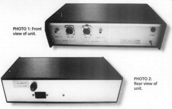
PHOTO 1: Front view of unit. PHOTO 2: Rear view of unit.
This allows for short speaker cables, thus reducing the wire impedance, but the signal between pre amp and amplifier must traverse a much longer distance.
Standard unbalanced audio signals can be degraded by power-line hum and noise pickup if the shielded interconnects are much more than 6" long. Be cause the shield carries the signal return, it can pick up any hum or noise and inject it into the audio signal.
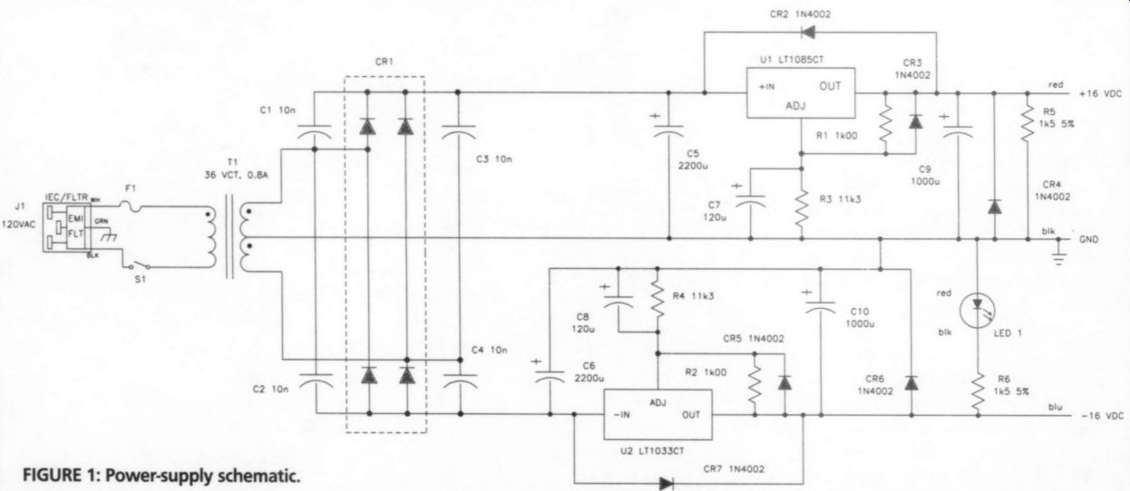
FIGURE 1: Power-supply schematic.
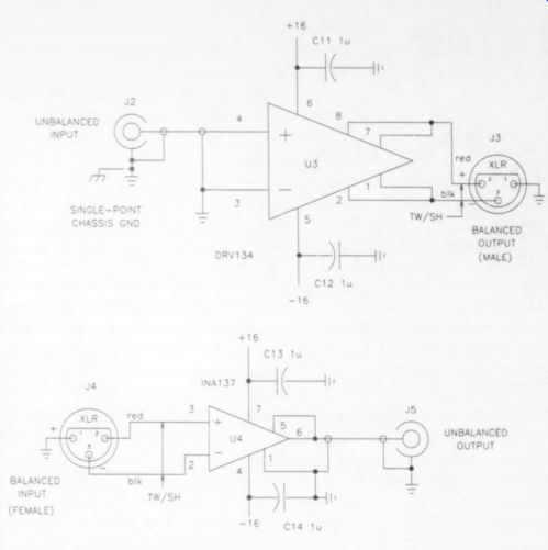
FIGURE 2
-------------
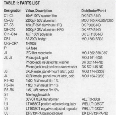
TABLE 1: PARTS LIST
Designation Value, Description Distributor/Part # C1-C4 10nF 100V stacked film DKP4713-ND C5-C6 22004F 50V aluminum MOU 140-XRL c7-C8 120uF 35V aluminum HFQ DK P5698-ND C9-C10 1000pF 35V aluminum HFQ DKP5743-ND C11-C14 1uF 100V polyester DKEF1105-N CR1 3A 200Vbridge MOU 583-BR32 CR2-CR7 1N4002 F1 1A fuse J IEC filter receptacle MOU 562-858-0 32,05 Phono jack, gold MOU161-4003 Phono-jack insulated flat-washer DK SC1144-N Phono-jack insulated extrusion washer DK SC1145-ND 3 3XLR male, pane-mount latch, gold ~~ MOU174-7230 J XLR female, pane-mount latch, gold ~~ MOU 164-7220 R1-R2 1k00, %W metal fim1% R3-R4 11k3, %W metal film1% R5-R6 1K5, %2W carbon film5% st Mini-toggle switch m 36VCT 0.8A transformer ALL TX-3608 ut LT1085CT positive-adjusted regulator ~~WELLT1085C u2 LT1033CT negative-adjusted regulator WELLT1033C U3 DRV134P; A balanced driver DKDRV134P at
Drafting appliqué film (Letraset Letra copy Creative or Chartpak DAF8), available at art- or drafting-supply houses.
----------------
Project enclosure, fuse holder, printed-circuit material, nylon spacers, LED mounting ring, hook-up wire, shielded audio cable, two-pair twisted/shielded audio cable solder, hardware, and so on.
--------------
If the unbalanced line-level audio signal is converted to a balanced signal, you can send it over much longer lengths of audio cable without degradation. This is so be cause a balanced audio cable carries two equal but out-of-phase signals, with neither connected to ground. Any hum or noise is picked up equally on both lines.
A differential amplifier at the receiving end of the cable rejects the hum and noise by common-mode rejection. The common-mode rejection ratio (CMRR) of the differential stage determines the amount of rejection after the signal is converted back to unbalanced form.
Of course, the active circuitry used for the balanced-to-unbalanced conversion also degrades the signal to some extent.
However, this is true whether the balanced circuitry is incorporated in the preamp/amplifier or added externally.
Some audio gear with balanced inputs or outputs merely adds a phase-inverter stage to produce or receive the inverted portion of the signal. In any case, it is important to use high-quality devices de signed specifically for audio applications (more on this later).
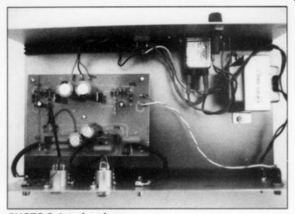
PHOTO 3: Interior view.
Quality unbalanced audio coax inter connects with RCA-type phono plugs are usually limited to a distance of 2m (6.6), although I have seen cheap 50' stereo pairs with molded cadmium-plated phono plugs for about $5. Caveat emptor! Good-quality balanced two-conductor shielded audio interconnects and microphone cables with XLR connectors are readily available in 20" lengths.
How It Works
The schematic diagram for the Audio Balun power supply is shown in Fig. 1, and is essentially the same circuit Gary Galo designed for his Preamp Power Supply (TAA 4/90, p. 47). The parts list for the complete unit is shown in Table 1.
The 36V AC secondary winding of T1 is full-wave rectified to +/- 24V DC. IEC filter receptacle J1 and capacitors C1-C4 filter the rectification noise from CR1.
Capacitors C5 and C6 filter the rectified DC that is applied to linear regulator ICs Ul and U2. R1-R4 set the power-supply rails to +/- 16V DC, and C7-CS8 filter noise from the adjust pins. C9 and C10 filter the output of the regulators, and CR2-CR7 prevent damage to the ICs if a short should occur in the unit.
In addition, the supply rails to ICs U3 and U4 are locally bypassed with 1uF film caps as recommended by the application notes. The only chassis ground connection for the audio circuitry is at the unbalanced input jack, J2. Insulators are used on unbalanced output jack J5 to isolate it from the chassis, thus preventing any ground loops. R5 mimics the power-supply load provided by R6 and power-on indicator LED 1, and fuse F1 protects the power supply.
The audio conversion circuitry is shown in Fig. 2. The unbalanced-to-balanced signal conversion is performed by U3, a Burr-Brown DRV134 audio balanced line driver, with the following specifications:
CMRR, 46dB min (68dB typical) at 1kHz and 600 ohm load;
* Symmetry of balance (SBR) of 35dB between the two balanced signals;
THD+N, 0.001% from 20-20kHz, 10V RMS output;
Slew rate, 15V/us typical;
* Noise floor, -98dBu; and
* R,, 10k - 2k, R 5 0-Ohm per side.
The balanced-to-unbalanced signal conversion is performed by U4, a Burr Brown INA137 audio differential line receiver, with the following specifications:
CMRR, 74dB minimum (90dB typical) at 1kHz and 600 load;
THD+N, 0.0005% from 20-20kHz, 10V RMS output;
Slew rate 14V/uS typical;
* Noise floor, ~106dBu;
* R,,, 24k differential, 18k common mode; and
* Output-current limiting, +t60mA.
You can connect the INA137 for a gain of V2 or 2 (x6dB). I used it with a gain of 12, so a full unbalanced-balanced-unbalanced conversion will have unity gain. If you wish, you can configure IC4 for a gain of 2, or use the similar INA134 audio differential-line receiver, which has unity gain. (Note that these are not equivalent to the professional audio impedance conversion of +4dBm 600-Ohm to --10dBv 2k IHF load.) Burr-Brown designed these devices as improved pin-compatible versions of the Analog Devices' SSM2142 balanced-line driver, and the SSM2141 and SSM2143 differential-line receiver chips. Data sheets for all the ICs are available at the Burr Brown website as PDF file (burr-brown.com). I suggest you download them so you can avail yourself of the application notes, test data, and test methods for these devices.
Both ICs are fully protected for continuous short circuits from output to ground I used the AES standard connections for XLR balanced OGY connectors J3 and J4: pin 1 ground, pin 2 normal ("hot"), and pin 3 inverted.
Construction
I used a Sescom MC-25A chassis for this project. I like working with the Sescom enclosures-each surface is an individual flat aluminum panel, which makes ma chining very easy. You are never working down inside a "tub." The total parts cost for the project comes to about $95.
Figure 3 shows the top and front views of the Audio Balun chassis layout.
All the wiring on the power-supply side is twisted to minimize magnetic fields, which could induce noise or hum. The transformer has a complete steel shield around the core, and is potted to reduce mechanical noise. An interior view of my unit is shown in Photo 3. Note that you could use an IEC receptacle with an integral fuse instead of my separate receptacle and fuse holder.
The two XLR connectors require 0.953" chassis holes. I used a 1" chassis punch, and, with some judicious locating of the mounting screws, the flange of the connector just hid the hole.
Figure 4 shows the lettering designations for the front panel. I made a full size copy of this lettering on drafting appliqué film, which is an adhesive-backed transparent plastic (see parts list). A light-color base paint is required, since the photocopy lettering is black, al though you can change the letter colors if you use a color cartridge in the copier.
Apply the lettered film to the front of the unit in the proper locations. Cut through the film at the drilled holes and then spray it with two coats of clear polyurethane for protection.
The four snubber caps, C1-C4, are mounted on bridge rectifier CR1, which is, in turn, mounted on the chassis be hind the circuit board, a single-sided, blank copper PCB as shown in Fig. 5 and Photo 4. The outline drawings for the semiconductors are shown in Fig. 6.
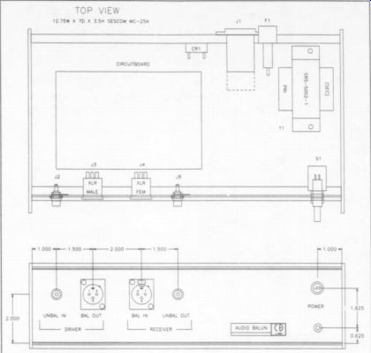
FIGURE 3: Chassis.
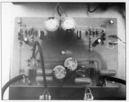
PHOTO 4: Circuit-board close-up.
Track-Routing
I routed many of the tracks directly, using a Dremel router with a 0.046" metal-cutting bit. For the resistors and the input/output pins, I drilled holes for standard T49 wire-wrap pins. The board is oriented with the copper side down. Wherever the pins are connected to circuit ground, I soldered them to the cop per ground plane. Wherever they are not grounded, I used a Vector P138A pad cutter to cut an electrically isolated circular pad on the copper around each 0.042" (#58 drill) hole. (The pad cutter is available from Mouser as p/n 574 P138A.)
I then wire-wrapped the sockets for U3 and U4 as though I were using a standard pre-punched vector board. This gave me the advantage of a ground plane with out the messy etching process needed for creating a printed wiring board. I placed the resistors on T49 pins so I could set the power-supply rails to exactly +/- 16V DC and adjust the quiescent-supply loading.
In keeping with good assembly practice, install the least sensitive parts first, followed by those more sensitive. Begin by soldering the passive parts (resistors then capacitors). Finally, install the semi conductors. Double-check the orientation of the polarized components. I used sockets for U3 and U4, and checked the power-supply voltages at the IC pins be fore installing them.
All circuit-board mounting holes have sufficient clearance for a 4-40 screw with flat washer. I used five "long tapped nylon spacers to mount the board to the chassis--3/4" spacers because of the height of the wire-wrap pins.
Figure 5 also shows the wiring to parts located off the circuit board. After installing the mechanical parts in the chassis, place the board near its final lo cation and then wire to the switch, LED and jacks. Since the rails of the enclosure are anodized (nonconductive) I connected the IEC third-pin ground wire to the IEC connector mounting screw, and used the transformer-frame mounting screw to tie these two panels together. I also connected the single-point ground connection to the front panel at the flange grounding tab for J3.
Run a separate-signal ground wire from the ground lug of J1, which is also the single-point chassis ground, to the circuit board. Use shielded wire from the phono jacks to the circuit board, and twisted/shielded pairs from the XLR jacks to the board. The purpose of all these single-ended ground and shield connections is to prevent ground loops and noise currents on the shields, which could couple into the signal. Finally, after all wiring is complete, install the board in its final location.
Using the Audio Balun
As I mentioned in the beginning of this article, I use the Audio Balun for making measurements on audio equipment with balanced inputs or outputs. You will need to build two units with double the driver-receiver circuitry if you intend to use the design in a stereo audio system. One unit will contain two DRV13 driver ICs and a power supply. The INA137 is available as a dual device in a 14-pin DIP package as the INA2137P so the second unit can contain one INA2137 and a power supply. A block diagram for this stereo arrangement is shown in Fig. 7.
For those of you interested in surface mount, all the power-supply, driver, and receiver ICs mentioned here are also available in small outline packages.
Measurements I took some audio measurements for a full unbalanced-balanced-unbalanced conversion, from the unbalanced input of the DRV134 to the unbalanced output of the INA137 (J2-J5). The two XLRs (J3 and J4) were interconnected with a 20 twisted/shielded balanced microphone cable.
-----------------
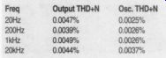
TABLE 2: THD+N VS. FREQUENCY, 1 VRMS
Freq Output THD+ N Osc. THD
20Hz 0.0047% 0.0025% 200Hz 0.0039% 0.0026% kHz 0.0049% 0.0026% 20kHz 0.0044% 0.0037%
-------
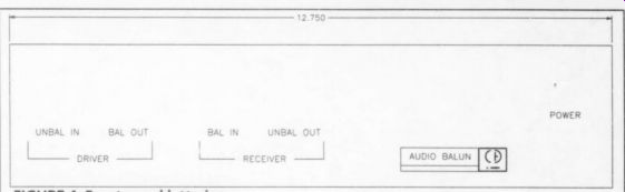
FIGURE 4: Front-panel lettering.
------
To remove out-of-band noise, I measured the THD+N from J2 to J5 with the distortion-test-set 80kHz low-pass filter engaged. Table 2 shows the results with a 1V RMS input signal to the Audio Balun. The test-set oscillator THD+N is also listed for reference.
----------------
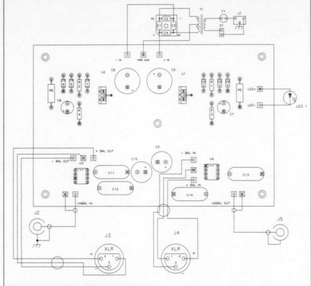
FIGURE 5: Circuit-board layout and wiring.
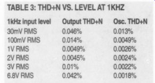
TABLE 3: THD+N vs. LEVEL AT 1 KHZ
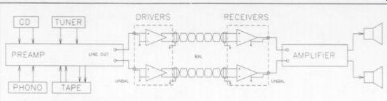
FIGURE 7: Driver/receiver stereo connections.
My second test was THD+N versus input level, from 30mV RMS to the maximum test-set signal level of 6.8V RMS, all at 1kHz. Again, the distortion-test-se 80kHz low-pass filter was engaged. The data is shown in Table 3.
I viewed the J5 distortion residual waveform at the monitor output of the distortion test set, after the fundament notch filter. The distortion products were second and third harmonics over laid with some noise.
I repeated all the THD+N measurements at balanced output jack J3. The THD+N was identical to the prior tests showing no decrease even with the distortion-test-set 30kHz low-pass filter en gaged. This indicates that the performance of the unit is limited by distortion products (as opposed to noise) generated by the DRV134. The THD+N at J5 with a 1kHz 1V RMS input signal remained below 0.005% with loads from 100k down to 25 ohm. With lower load resistances, the INA137 went into current limiting, and distortion increased. The unbalanced input impedance to J2 (the DRV134) measured 8k5.
Overall frequency response (J2-]5) was ruler flat from 10Hz to 100kHz. The output signal was consistently 0.67dB higher than the input signal (1.08V RM output for a 1.0V RMS input signal). The output level at J3 was 2.16V RMS, indicating that the 0.67dB gain error was generated in the DRV134. The difference between the J3 pin-2 and pin-3 outputs (referenced to pin 1) was only 9mV (0.07dB Response was independent of output loading from 100k down to 20 0-Ohm. In fact, the output at J5 wasn't down 50% until an extremely low output load of 1 0-Ohm, where distortion was over 10% and the INA137 output was in current limiting.
Output noise with J2 shorted was 25uV RMS, or -90dBu, with no evidence of 60Hz powerline hum or its harmonics. Visible clipping occurred at J5, when the output reached =14.5V pk-pk, or about 10.5V RMS.
The response to a 1V pk-pk square wave at 40Hz and 1kHz was just about perfect. The 10kHz square wave showed a single damped peak on the leading edge, which did not change with loads from 1M (scope input) down to 100. The time for this half-cycle peak corresponded to a frequency of about 1-MHz.
Also see: