Discrete transistor circuitry and integrated circuits ( ICs) are common place in modern broadcast installations. This is true not only for audio amplifiers but for control circuitry such as switch gear, transmitter remote control, and automation facilities as well. Low-power rf stages in transmitters are now almost completely solid state.
NOTE: The reader should have basic solid-state training at least equivalent to the author's Workshop in Solid State. The fundamentals of semiconductor circuitry most important to the am-fm broadcast technician will be reviewed in this Section. As developed in the above-mentioned reference, we will refrain from the equivalent-circuit approach, which involves h parameters and complex mathematical analysis, and emphasize a much simpler circuit analysis with practical applications. We will then study the principles of logic circuitry most often found in various applications in am-fm broadcast installations.
---Harold E. Ennes, Workshop in Solid State (Indianapolis: Howard W. Sams & Co., Inc., 1970).
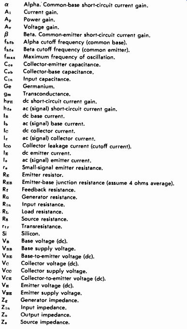
Table 3-1. Symbols Used in This Guide
a Alpha. Common-base short-circuit current gain.
At Current gain.
AT, Power gain.
A.- Voltage gain.
B Beta. Common-emitter short-circuit current gain.
f Alpha cutoff frequency (common base).
fhfe Beta cutoff frequency (common emitter).
Maximum frequency of oscillation.
C.e Collector-emitter capacitance.
Ce5 Collector-base capacitance.
Co Input capacitance.
Ge Germanium.
gm Transconductance.
Firs dc short-circuit current gain.
hr. ac (signal) short-circuit current gain.
In dc base current.
In ac (signal) base current.
le dc collector current.
I. ac (signal) collector current.
lco Collector leakage current (cutoff current).
le dc emitter current.
I. ac (signal) emitter current.
r. Small-signal emitter resistance.
RE Emitter resistor.
Res Emitter-base junction resistance (assume 4 ohms average).
lb Feedback resistance.
Re.. Generator resistance.
Rt Input resistance.
RL Load resistance.
Rs Source resistance.
rtr Trans resistance.
Si Silicon.
Vn Base voltage (dc).
Vnn Base supply voltage.
VHF; Base-to-emitter voltage (dc).
Ve Collector voltage (dc).
Vee Collector supply voltage.
Vee; Collector-to-emitter voltage (dc).
VF: Emitter voltage (dc).
VEE Emitter supply voltage.
ZK Generator impedance.
Zi Input impedance.
Z. Output impedance.
Z Source impedance.
3-1. BASIC PARAMETERS OF SOLID-STATE AMPLIFIERS
There are certain practical parameters that are common to all solid-state amplifiers. If the maintenance technician is sufficiently familiar with these characteristics, he knows almost exactly what to expect in waveform and voltage analysis, regardless of what make of amplifier or control circuit he is troubleshooting.
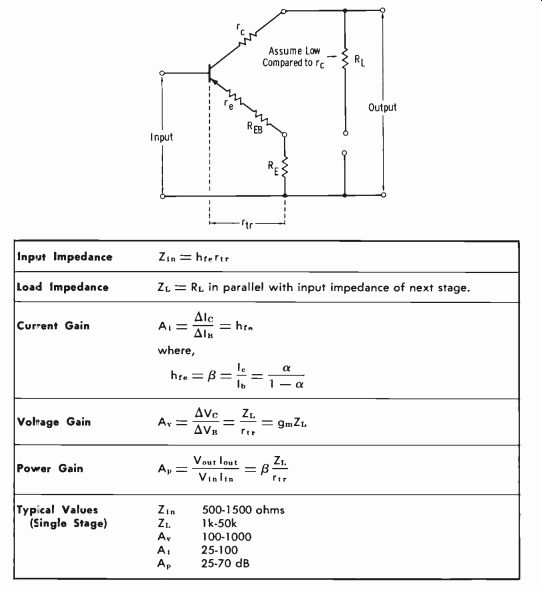
Chart 3-1. Basic Parameters Common to All Configurations

Chart 3-2. Parameters of Common-Emitter Circuit
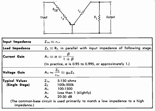
Chart 3-3. Parameters of Common-Base Circuit
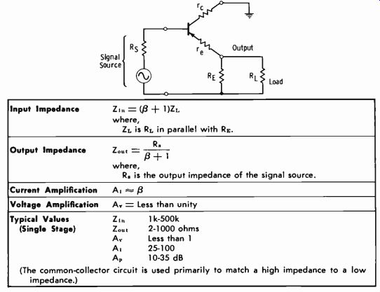
Chart 3-4. Parameters of Common-Collector Circuit
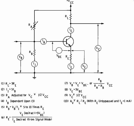
Fig. 3-1. Design parameters for common-emitter amplifier.
Table 3-1 lists the symbols used in this study, and Chart 3-1 gives the basic parameters common to all circuit configurations-common emitter, common base, and common collector (emitter follower). Charts 3-2, 3-3, and 3-4 give the specific parameters for the common-emitter, common-base, and common-collector configurations, respectively.
The Common-Emitter Amplifier
The common-emitter circuit (Fig. 3-1) is by far the most widely used in amplifier design. The common-base circuit is most often used to match a low impedance to a high impedance, and the common-collector (emitter-follower) circuit is most often used to match a high impedance to a low impedance.
The design parameters for Fig. 3-1 apply to a stage intended for linear amplification, as revealed by the fact that the quiescent collector voltage (Ve) is fixed to the approximate midpoint between ground and full collector supply voltage (Vcc) . Some form of stabilizing feedback is normally provided, and we will examine this basic characteristic now.
Emitter Feedback
Emitter feedback is, very simply, the result of the unbypassed emitter resistor, RE. Since the signal induced in useful collector load RL must pass through RE, the signal is degenerated. This type of feedback is a form known as series feedback, and it increases the input impedance. Before we go further, it is important to examine in more detail this most common form of feedback stabilization.
First, let us put down applicable relationships for the circuit of Fig. 3-1 for future reference:
VBE = 0.2 to 0.3 V for germanium transistors
VBE = 0.6 to 0.7 V for silicon transistors
IE IB =-- 'co 11FE (Eq. 3-1) (Eq. 3-2) ( Eq. 3-3)
Ic = aIE Ic=IE- IB Ic = hFEI$ Zin- hFFxtr Zload = RL in parallel with following-stage input Z Ai=hFE Ri.
A°
_ rtr A = gn,RL An= (Ai)'RL =A,A =RRi.
Rrtr rtr
( Eq. 3-4) ( Eq. 3-5) ( Eq. 3-6) ( Eq. 3-7) ( Eq. 3-8) ( Eq. 3-9) ( Eq. 3-10) (Eq. 3-11)
( Eq. 3-12)
Now study the ten points listed on Fig. 3-1. They show how the design engineer arrives at stable operating parameters for a linear (class-A) amplifier.
In point 6, it is stated that the emitter current desired is derived from the intended operating mode. For example, a low-level stage (such as an audio preamplifier) must be operated at very low emitter (hence base and collector) currents in the interest of low noise level. As the signal level is brought higher and higher in amplitude, more and more dc current must be employed to accommodate the higher peak-to-peak signal swings.
The main problem in stabilization is to control the current gain (Beta, or hFE) of the common-emitter circuit. The actual value of Beta differs with different transistors of the same type, and it also varies with temperature changes. Consequently, practical circuit design requires a controlled beta (controlled current gain) so that this parameter will remain fixed under varying operating temperatures and with necessary transistor replacements.
Thus, if a certain transistor type has a "minimum hFE" of 20, the circuit is designed to limit beta to no more than 20 by means of fixed resistance ratios.
We can now examine a practical single-stage common-emitter linear amplifier and see how such a design is made. Let us analyze the circuitry in Fig. 3-2 for practice in determining what we should expect in dc voltage measurements, and to see how it meets the design requirements of Fig. 3-1.
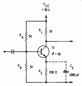
Fig. 3-2. Class-A common-emitter amplifier circuit.
Step 1 is to determine the base voltage, VB. We can do this by figuring the current in RB, or we can use the second relationship of item 7 in Fig. 3-1. In either case, VB = +5 volts.
Then, since the transistor is a silicon (Si) type:
VE = +5- 0.6 = +4.4 volts (Note that this value is greater than 5 times VBE, as called for in Fig. 3-1.)
Since the emitter voltage is +4.4 volts, the emitter current (from Ohm's law) must be:
2 IE= 00=22mA
For rapid analysis, assume the same current in the collector as in the emitter:
1o= 22 mA
Then the dc voltage drop across RL is:
VRL = (0.022) (1000) = 22 volts and:
Ve=50-22=+28 volts (Note that this value is close to 1/2 Vee. )
For the given transistor, hFE = p= 50.
Then, from equation 3-3 (ignoring Ico)
IB=O'002-0.44mA
Note that current I1 is 5 mA and therefore meets the requirement of being more than 5 times the base current (IB) .
With RE bypassed (CE connected) :
Ai = hFE = 50 ( from specification sheets) 26 rt`=22+4=5 (approx) RL 1000 200 rtr 5 Z;,, _ (50) (5) = 250 ohms ( from equation 3-7)
Note that since RE is bypassed for the signal, the signal is not degenerated. Therefore, the full value of beta is in effect, with the exception of the slight shunting action of bias resistors RA and RB.
Now consider the case in which RE is not bypassed by CE. The first change to note is the effect on input impedance Z1 of the transistor alone.
When RE was bypassed, Z1 equaled 250 ohms. But when RE is not by passed, rtr becomes 205 ohms, or approximately 200 ohms. Then:
Z1 _ (50) (200) = 10,000 ohms
Now it is evident that the value of RB essentially fixes the value of the new input impedance. Since R1 is only one tenth of the transistor input impedance, the current gain will be reduced drastically.
For practical circuit analysis, the following relationship of currents and resistances is sufficiently accurate:
Ie-RB RE
This equation says that the emitter current is to the input current as base resistor RB is to emitter resistor RE. From this basic relationship, we can derive a useful equation for quickly evaluating current gain in a degenerative amplifier. Since collector current (for rapid estimates) can be considered to be the same as emitter current, then substituting I, (collector current) for Ie (emitter current) in the above basic equation:
I,.
- RB
- Ii.. RE
Note that the ratio of Ie (collector current) to Ii (input current) is an expression for current gain (Ai) . So:
Ai = R" (for an unbypassed RE) (Eq. 3-13) Note also that when an unbypassed RE is much greater than re + REB, voltage amplification (AT) can be expressed:
Rt A,. = (for an unbypassed RE) (Eq. 3-14)
This equation is valid so long as re + REB is very small in value compared to RE and can be ignored.
Based on the above equations, the new current gain with RE unbypassed is:
Ai_RB_1000_5 RE 200 and the new voltage gain is:
R1 1000
RE 200
Other Basic Negative-Feedback Circuits
Although emitter degeneration (series feedback) is almost universally used, other forms of degenerative feedback, which may or may not be used along with emitter degeneration, are often encountered. We will explore briefly the fundamentals of such circuitry.
The basic arrangement for collector-base feedback (termed shunt feed back is shown in Fig. 3-3. For most practical circuits, the resistance of Rf is small enough that we can use these approximate gain formulas for quick-analysis purposes:
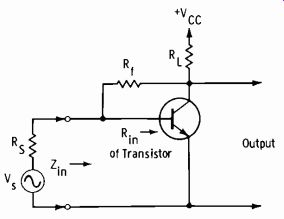
Fig. 3-3. Circuit with shunt feedback.
(Eq. 3-15)
(Eq. 3-16)
The quantity Zin, the effective input impedance of the stage, is approximately:
Rf RRL Rf Rill ( Eq. 3-17)
... where Rin is the input impedance without feedback.
Note that shunt feedback decreases the effective Zin, whereas series feed back ( such as that provided by an unbypassed emitter resistor) increases the effective Zin.
NOTE: The gain formulas given above are adequate for quick analysis of most circuits because Rf is usually relatively low in value to meet the requirement of "adequate feedback." Somewhat more nearly exact relation ships are as follows:
Rf Al /3 A Rf Rr.
Rf Rj
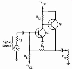
Fig. 3-4. Diagram of a feedback pair.
Fig. 3-4 shows a "feedback pair." This circuit is gaining universal acceptance as a stable, wideband amplifier with inherent ac and dc stability. This type of circuit has low input and output impedance. For quick analysis, its voltage gain can be calculated from the expression:
A,. = Rft (Eq. 3-18)
... where RA is the output resistance of the signal source. This formula is sufficiently accurate for use in normal applications of the circuit with low input and output impedances. The voltage gain is almost universally held to a value less than 10.
Feedback Gain-Impedance Relationships
We should be certain of a "sharp focus" on impedance-to-gain relation ships. For example, series feedback affects voltage gain much more than current gain, and shunt feedback affects current gain much more than voltage gain. These facts always bring up the question, "If you cut current gain, how can voltage gain remain the same?" Or, "If current gain is not affected, why does voltage gain decrease?" This discussion should answer these questions.
See Fig. 3-5A. This circuit is without negative feedback. Assume that:
Ai=hfe=50 Input signal current = 10 µA
Effective Z10 = 1000 ohms (resistive) RL = 2000 ohms
Then:
Signal current in RL = (50) (10 µA) = 500 µA.
Signal voltage in Zin = IR = (10 µA) (1000) = 0.01 volt
Signal voltage in R1, _ (500 µA) (2000) = 1 volt
Fig. 3-5. Comparison of shunt and series feedback. (A) No feedback.
(B) Shunt feedback. (C) Series feedback.
Ao Vout 1 = 100 V,u 0.01
Now see Fig. 3-5B.
Shunt feedback is used, and:
A1 is cut to 10 (from 50).
Signal input current is maintained at 10 µA ( for reference) .
Rin is reduced (by shunt feedback) from 1000 ohms to about 200 ohms (from equation 3-17) .
Now:
Signal current in RL = (10) (10 µA) = 100 µA= 0.1 mA.
Signal voltage in RL = (0.1 mA) (2000 0) = 0.2 V = 200 mV.
Signal voltage in R10 = (10 µA) (200 II) = 0.002 V= 2 mV.
_200 mV
A° 2 mV = 100 (the same as for the circuit of Fig. 3-5A) .
Note that although the output signal voltage was reduced in amplitude for the same signal input current, the voltage amplification remained the same for the circuit of Fig. 3-5B as for that of Fig. 3-5A. The current amplification is limited to 10 (which will be below the minimum beta of the transistor used) so that voltage output is stabilized for changes in hre.
As a matter of interest, the voltage gain calculated from the more complete equation given in the note above is:
20K 2K A` 2K+20K(50)1K=90
The "quick-analysis" value is within about 10 percent of this result.
Fig. 3-5C shows the series-feedback arrangement of the common-emitter circuit. Whether bypassed or not, RE has no effect on the current-gain parameter of the transistor. But we already know that it drastically affects the voltage gain of the circuit.
Assume that RE is bypassed and that the signal input is 10 microamperes.
Then:
Signal current in RL = (50) (10 µA) = 500 µA
Signal voltage in RL = (500 µA) (2000 II) = 1 volt
Signal voltage in Rio = 10 µA (hrertr) = 10 µA )(-1.626
= 10 µA (1000 S2) = 0.01 volt A" 0.01= 100
Now assume that RL is not bypassed ( series feedback to signal) :
Ri = 50 (20 + 200) = 10,000 ohms (approx) Vio= (10µA) (10,0001) =0.1 volt Signal current in RL = 50 (10 µA) = 500 µA (hre not changed)
Signal current in RL = (500 (2000 St) = 1 volt A = 011= 10 as RE = 2000- 10) It has been pointed out that hFE is the dc beta (common emitter) and that hre is the ac, or signal, beta. This difference can be emphasized by studying Fig. 3-6.
The circuit of Fig. 3-6A is equivalent to a single stage that has a 5K collector load and is feeding a following circuit with a 1.5K input impedance. At low frequencies, the load resistance is effectively 5000 ohms. Assume hFE = hr. = 50. The output voltage swing for a base-current swing of (for example) 3 microamperes is:
V= (3µA) (50) (5000 Si) =750mV
(A) Dc load. (B) Ac load.
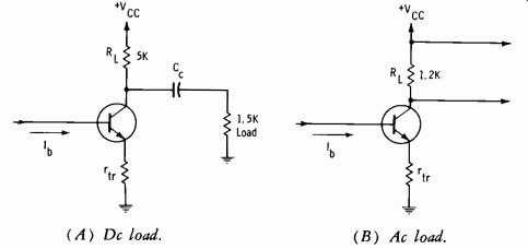
Fig. 3-6. Circuit equivalents for ac and dc gain.
At high frequencies (for which the reactance of Co can be neglected) , the effective load becomes 5K in parallel with 1.5 K, or about 1.2K (Fig. 3-6B). Now the output-voltage swing for a 3-microampere base-current swing is:
V= (3µA) (50) (1200íL) = 180 mV
This example simply emphasizes that with life equal to hFE, the actual voltage swing is much less for hte due to the difference in the load the transistor sees.
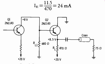
Fig. 3-7. Typical emitter follower.
The Common-Collector (Emitter-Follower) Circuit
The emitter follower is used extensively for applications in which a low output impedance is desired. Fig. 3-7 shows an output stage driving a 75 ohm coaxial line, as used in certain forms of control circuitry. The 8 volts on the base is developed across the collector load of Q1. The emitter measures 8.5 volts, so the voltage drop across RL is 20- 8.5 = 11.5 volts.
Therefore: 1F=470= 24 mA
The transistor has a typical t3 of 50; therefore:
IB = I,; 0.024 480 µA Il E 50
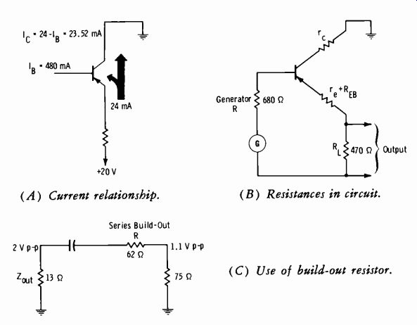
Fig. 3-8. Basic analysis of emitter-follower stage.(A) Current relationship.
(B) Resistances in circuit. (C) Use of build-out resistor.
It can be seen that a current gain (480-12A base current to nearly 24-mA collector current) occurs in the emitter follower just as in the common-emitter amplifier (Fig. 3-8A) . But the voltage gain is approximately unity.
The output signal is of the same amplitude as the input signal, less a very small signal-voltage drop across the base-emitter junction. The voltage gain of this circuit can be explained as follows:
The effective R1, (the load presented to the signal voltage) in this case is the 75-ohm line termination in parallel with 470 ohms, for an effective RL of 65 ohms. The trans-resistance (rtr) is:
rtr= 16+REB-RL
= 1 (approx) + 4 + 65 = 70 ohms
Then, since gn, is 1 1/70, or 0.014:
rtr Ar=gmRi,= (0.014)(70)=)0.98
Or, we can say that, since RL is much greater than re + REB:
A,. = RL (approx) In this case, RE = RL, so:
A, = 17 = 1 (approx)
In practice there are many cases in which it is not possible to measure any amplitude difference between the signals at the base and emitter of a common-collector stage. For this analysis, we can delete REB from the gm computation. The gain may normally be assumed to be unity for quick circuit analysis. Note also that the dc parameters were used in the above analysis, so we are considering only low frequencies (and dc) at the present.
Study Fig. 3-8B, and observe that re-appears in parallel with the sum of re, REB, and RL. Since re can be assumed to be 1.5 megohms or more, it need not be considered for quick circuit analysis. What is important is to note that the actual input impedance and the output impedance are some what interdependent. This is true because the input load is part of the output, and the output load is part of the input. The high intrinsic value of re is not serving as isolation between input and output as it does for the other configurations; it now forms a parallel resistance only.
Since the emitter follower is used primarily as an impedance trans former, the input and output impedances are most important characteristics to know. While conventional treatments result in highly complex formulas, we can use the following rules of thumb that are fairly accurate in practice:
Zie= (f3+1)Rt, Rs Z"°t=Q+1
The input resistance of the stage in Fig. 3-8 is:
Zin = (50 + 1) 65 = 3300 ohms (approx )
This resistance has a reasonably small loading effect on the 680-ohm collector load of Q1.
( Eq. 3-19) ( Eq. 3-20) 680 Zet = 50 + ohms (approx)
The internal output impedance (sending-end impedance) of an emitter follower can be made quite low, sufficiently low to drive 2-ohm switching buses directly. This low impedance also is the reason why a series "build-out" resistor is usually used (Fig. 3-8C) . For the receiving end (75 ohms) to "see" a 75-ohm impedance, the 13-ohm output would require a series resistance of 62 ohms. Note also that this arrangement forms a voltage divider, and a 2-volt signal across RL is dropped to 1.1 volts across the 75 ohms.
In practice, as the effective load impedance increases, the input impedance increases. As the generator impedance increases, the output impedance increases. Providing the generator impedance (previous collector RL) is not extremely low (so long as it is greater than 10 times RL, as is usually the case) , the formulas given above will prove sufficiently accurate for practical purposes.
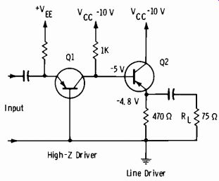
Fig. 3-9. Emitter-follower line driver.
Figs. 3-9 through 3-12 illustrate the basic applications of the common-collector configuration. In Fig. 3-9, the output impedance of Q1 is essentially the collector load of 1000 ohms. For class-A operation, we expect a quiescent collector voltage of 1/2 Vec =-5 volts. Assume germanium transistors with a beta of 50. Then the common-collector line driver, Q2, has:
470 (75) 65 ohms (effective load) 470 + 75 1000 Z°°` 50 + 1 =
20 ohms (approx) Z1, = (50 + 1) 65 = 3300 ohms (approx)
Now study Fig. 3-10A. In this case, the emitter-follower line driver is driven by an emitter follower. The 1K load is now in the emitter circuit of Q1 rather than the collector circuit. Let us see what happens. (Assume Q1 sees a source resistance of 1000 ohms, and Beta is 50 for both transistors.) The output impedance of Q1 is:
ZoUt 1000- 20 ohms (approx) 50 + 1
Then the output impedance of Q2 is:
Z011 t 520 0 + 1- 0.4 ohm (approx)
The equivalent circuit of the output stage is shown in Fig. 3-10B. Note that co feed a 75-ohm load, a build-out resistance of 75 ohms is needed so that the effective internal output impedance becomes 75 ohms. The build-out and load combine to form a 2:1 voltage divider. We must therefore expect to find the signal voltage at the emitter of Q2 to be twice as great as the signal voltage across the 75-ohm load. This condition is normal. For a 1-volt peak-to-peak signal to appear across the 75-ohm load, a 2-volt peak-to-peak signal must be available at the Q2 emitter.
(A) Schematic diagram. (B) Equivalent of output stage.
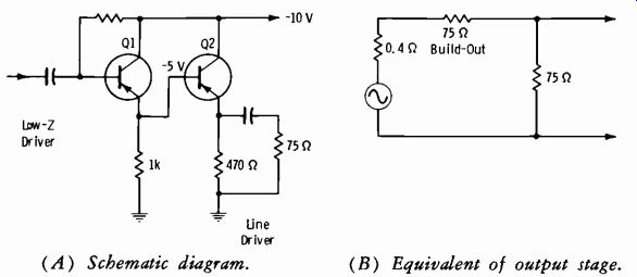
Fig. 3-10. Cascaded emitter followers.
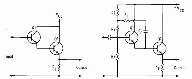
Fig. 3-11. Darlington circuit.
Fig. 3-12. Circuit with bootstrapping.
In solid-state circuit applications requiring a very high input impedance, the emitter follower is quite naturally chosen. The Darlington emitter follower shown in Fig. 3-11 consists of two current amplifiers in cascade to provide large current gain and very high input impedance. The input impedance is raised due to the effective product of the betas (hfe) of both transistors. That is, since the base currents have been reduced by the product of the current gains, the input impedance is raised accordingly.
The input impedance of the Darlington current multiplier is limited by the shunting effect of the Q1 collector resistance and capacitance. A technique for reducing this shunting effect is to employ positive shunt feed back, termed bootstrapping. In Fig. 3-12, the value of RF is such as to produce at the junction of R1 and R2 a voltage which is in phase with the input voltage. The signal-voltage drop across the bias resistors is thereby reduced, which is equivalent to raising the resistance of the input network.
Bootstrapping is used in other than Darlington circuits for the same reason to reduce the effective loading of the input biasing networks.
(A) Simplified diagram.
(B) Schematic symbols.
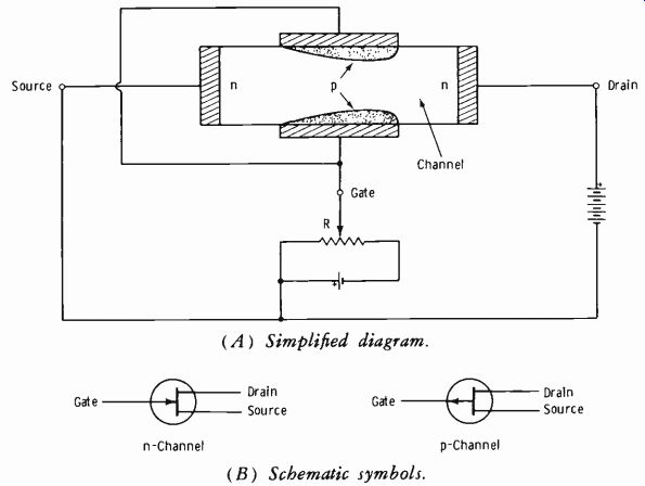
Fig. 3-13. Fundamentals of junction FET.
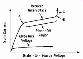
Fig. 3-14. Typical FET drain-current characteristic.
The Field-Effect Transistor
The field-effect transistor (FET) is a relatively new device, but it has gained substantially in practical applications. As with any device, it has advantages and disadvantages when compared to the conventional transistor.
For the conventional transistor, there are two major differences in operation compared to the vacuum tube; the input circuit must be forward biased (the tube is actually reverse biased) , and the output circuit must be reverse biased. So essentially we have a current-operated device (transistor) compared to a voltage-operated device (tube) . This is simply the most convenient way to contrast the two devices.
Now see Fig. 3-13A. In this junction type of FET, a pn junction is employed for the gate (control) electrode. The sole function of this gate is to provide a control element analogous to the grid of a vacuum tube. The FET also has a source (analogous to the cathode) and a drain (analogous to the plate). Note that the gate receives a voltage which is the reverse bias necessary to control majority-carrier current in the channel.
When the gate voltage is increased, the fields; setup by the junction barriers cause a reduction in the number of majority carriers flowing through the channel from source to drain (Fig. 3-14) . As the gate voltage is reduced, drain current increases. The area in which the drain voltage has á relatively small effect on drain current (between points A and B in Fig. 3-14) is termed the pinch-off region of operation. As the drain-to-source voltage is increased, or the gate voltage goes to zero bias or a slight forward bias, the drain current can increase excessively, and the FET can be dam aged by the resultant heating of the junction (part C of the curve in Fig. 3-14).
Just as with the vacuum tube, the input impedance of the FET in the common-source configuration is very high due to the reverse bias on the gate. The FET is advantageous to use where very high input impedances are required in a single stage of amplification. The device is extremely delicate in handling and servicing, but this disadvantage is rapidly being over come by "protected gate" design.
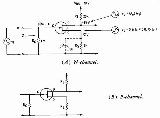
Fig. 3-15. Amplifier circuits using FETs. (A) N-channel. (B) P-channel.
Schematic symbols for the FET are shown in Fig. 3-13B. Figs 3-15A and 3-15B present a circuit drawn for an n-channel and a p-channel FET. The gate input impedance is normally around 10 megohms, and a fixed resistor (RG) is used so that the input signal voltage (vi) is developed across a known load for all frequencies concerned.
Typically, the signal at the source (v) will be between 0.6 and 0.75 of vi when Re is not bypassed. Resistor Rs supplies the proper bias to the gate and (for class A operation) fixes the drain voltage at about 1/2 of VDD.
The drain signal output (vd) is inverted.
Just as Beta = 50 is a good "average for the conventional transistor, so the transconductance (gm) for the proper operating point of the average FET can be assumed to be g_m = 500 micromhos, and Av = gm RL (approx) without feedback.
NOTE: In an FET, gm varies with drain current just as the beta of a conventional transistor varies with collector current. Therefore, it is subject to wide variation, and data sheets must be consulted to determine g_m at a specified drain current.
The voltage amplification with source feedback (C not connected) is:
gRr.
A. = m (approx) 1 + g_m R,
For the circuit of Fig. 3-15A, assume that gm = 500 micromhos. Then the gain without feedback is:
A. = (0.0005) (20,000) = 10 (approx)
With C not used (source feedback) :
0.0005 (20,000) 4 (approx )
Av 1 + 0.0005 (3000 )
Fig. 3-16 shows symbols for three types of metal-oxide-semiconductor FET (MOSFET) . These transistors are treated further in applicable portions of following Sections.
The characteristics of FETs may be summarized as follows:
1. High impedances permit use of vacuum-tube biasing techniques.
2. Very good thermal stability.
3. Extremely low feedback capacitance.
4. Low noise figure (nf = 3.5 dB, typical) . A noise figure of 5 dB is considered very good for conventional transistors.
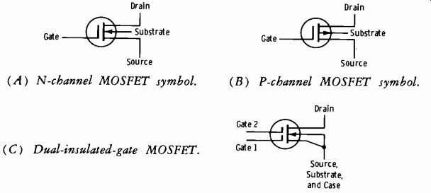
Fig. 3-16. Schematic symbols for MOSFETs. (A) N-channel MOSFET symbol. (B)
P-channel MOSFET symbol. (C) Dual-insulated-gate MOSFET.
Class-B Audio Operation of Transistors
Qass-B push-pull power amplifiers are used mainly in equipment that must provide high power output and high power efficiency. Fig. 3-17A shows a simplified circuit of a class-B amplifier. The emitter-base junctions are zero biased. In this circuit, each transistor conducts on alternate half cycles of the input signal. The output-signal half cycles are combined in the secondary of the output transformer. Maximum efficiency is obtained even during idling periods (no input signal) , because neither transistor con ducts during these periods.
An indication of the output current waveform for a given signal current input can be obtained by considering the dynamic transfer characteristic for the amplifier. It is assumed that the two transistors have identical dynamic transfer characteristics. The characteristic for one of the transistors is shown in Fig. 3-17B. The variation in output (collector) current is plotted against input (base) current under load conditions. Since two transistors are used, the overall dynamic transfer characteristic for the push-pull amplifier is obtained by placing two of the curves back-to-back. The two curves are shown back-to-back and combined in Fig. 3-17C. Note that the zero lines of the two curves are lined up vertically to reflect the zero bias current. Note that severe distortion occurs at the crossover point ( the point where the signal passes through zero). This crossover distortion becomes more severe with low signal input currents. Crossover distortion can be eliminated by using a small forward bias on both transistors of the push pull amplifier.
(A) Schematic diagram.
(B) Single transfer characteristic.
(C) Combined transfer characteristic.
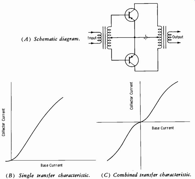
Fig. 3-17. Basic class-B amplifier. (A) Schematic diagram. (B) Uncombined transfer
curves. (C) Combined transfer curve.
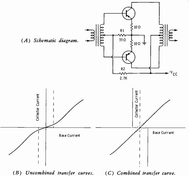
Fig. 3-18. Use of forward bias in class-B amplifier.
A class-B push-pull amplifier with a small forward bias applied to the base-emitter junctions is shown in Fig. 3-18A. A voltage divider is formed by resistors R2 and R1; the voltage developed across R1 supplies the base emitter bias for both transistors.
A study of the dynamic transfer characteristic curve of the amplifier demonstrates the elimination of crossover distortion. In Fig. 3-18B, the dynamic transfer characteristic curves of the two transistors are placed back-to-back (but not combined) for zero-base-current bias conditions.
The dash lines indicate the zero-signal point for each curve when forward bias is applied to the transistors. To obtain the overall characteristic (Fig. 3-18C), the two graphs are shifted until the dash lines meet; then the individual curves (dotted lines) are combined to form the solid curve.
Resistance-capacitance coupling to the input of a class-B push-pull amplifier cannot be used satisfactorily without special considerations. In the class-B push-pull amplifier, one transistor conducts during one half cycle of the input signal; the other transistor remains nonconducting during this time, except for the small forward bias applied to minimize crossover distortion. Refer to Fig. 3-19A. Assume that the input signal causes transistor Q1 to conduct. Electrons (solid-line arrows) leave the right-hand plate of coupling capacitor C1, enter the base-emitter junction of transistor Q1, flow to the emitter ground connection, go through ground to the junction of resistors R1 and R2, and pass through resistor R1 to the left-hand plate of C1. (Resistor R1 represents the output resistance of the previous amplifier.) Capacitor C1 charges rapidly through this low-resistance path.
However, C1 cannot discharge through the emitter-base junction of Q1; for practical purposes, the junction represents an open circuit to electron flow from emitter to base. Electrons on the left-hand plate of capacitor C1 must flow through resistor R1, through ground to the emitter connection of Q1, and through resistors R6 and R3 to the right-hand plate of C1. (The discharge path is shown by the dash-line arrows.) Capacitor C1 discharges slowly because it must discharge through R3; normally the resistance of R3 is made large to avoid shunting of signal current around the Q1 base emitter junction. The discharge current through R3 develops a reverse-bias voltage with the polarity indicated. The reverse bias can cause class-C operation with resultant severe distortion of the signal. (The discharge current through resistor R6 does not result in a reverse bias because the battery current in the opposite direction through this resistor maintains a forward bias.)
(A) Input resistors.
(B) Input diodes.
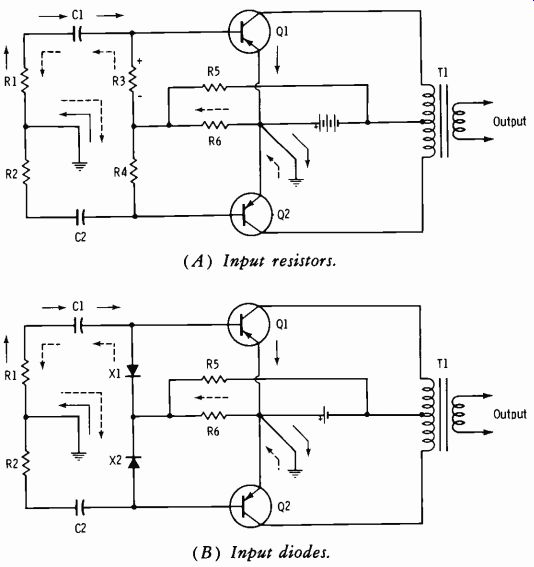
Fig. 3-19. Class-B amplifier with RC input coupling.
The advantages of RC coupling (economy and better frequency response) can be retained by replacing resistor R3 with a diode, as shown in Fig. 3-19B. Diode X1 is reverse biased and acts as a high-value resistance when the input signal has the polarity that causes the emitter-base junction of Q1 to conduct. This high resistance prevents the shunting of signal current around the emitter-base junction. The charge path (solid-line arrows) for capacitor C1 is the same as that for the circuit shown in Fig. 3-19A. In the discharge path (dash arrows) , resistor R3 is now replaced by diode X1, which is forward biased and has negligible resistance during the discharge period. Capacitor C1 discharges rapidly, therefore, and reverse bias of the emitter-base junction is avoided.
NOTE: The secondary windings of any class-B driver transformer (input to class-B stage) should be bifilar wound to obtain tight coupling and thereby minimize leakage inductance. Otherwise, "ringing" may occur in the crossover region as a result of the "kickback" energy stored in leakage inductance.
Now let us consider some power computations. By definition:
APP 2R1.
pt0 II Rt (Eq. 3-21)
Since, for a small load resistance, the ratio Io/ Iin is the same as beta (common-emitter circuit) , the power gain (which can be expressed in terms of the square of the current gain times the ratio of output to input resistance) can be expressed:
A=/12R- h' 1%-b-b (Eq. 3-22) where, Re, is the collector-to-collector load resistance, Rb_b is the base-to-base input resistance.
With this information, observe again Fig. 3-18A. Assume that the power-supply voltage is -12 volts, the impedance of the output-trans former primary is 300 ohms, center tapped, and the impedance of the in put-transformer secondary is 2000 ohms, center tapped. Assume a nominal beta of 50.
Then from Equation 3-22:
A= (50)22000- 2500(0.15) =375
What is the actual power output?
The rule of thumb is:
2 VVE2 Po =
Re_, (Eq. 3-23) In this equation, VoE is the collector-to-emitter voltage at no signal.
Remember that in a class-B stage, this voltage is very close to the power-
supply potential (close to current cutoff) ; it may be taken as about 85 percent of V. Thus, in this example, assume VcE =-10 volts.
Then:
2(-10)2-200_666mW P" 300 300
But remember that the power in the secondary depends on transformer efficiency, which normally may be assumed to be about 75 percent. So the actual power delivered by the secondary is (0.75) (666 mW) = 500 mW (approx).
Since the power gain is 375 and the power output (collector-to-collector) is 666 mW, then the required input power is:
P_out 666 mW 1.8 mW (approx) base-to-base A 375
An efficiency of 75 percent must also be assumed for the driver transformer, so the driver power must be:
P into input 1.8 mW 2 4 mW Pa`i."r
0.75 0.75
(A) Amplifier schematic
(B) Power-supply schematic.
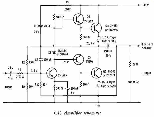
Fig. 3-20. "Single-ended push-pull" amplifier.
A good performance check of any amplifier is to determine how faith fully it reproduces a square wave. When a transformer is used, it must be physically large for good low-frequency response, and it must be of high-quality design and construction throughout. Therefore, a great deal of effort has been expended in developing "transformerless" push-pull circuitry. In tube circuits, a number of tubes must be used in parallel to obtain the necessary current to develop power in low-impedance devices such as the voice coils of loudspeakers. Power transistors, however, lend themselves ideally to this application since they are inherently low-voltage, high-current devices. Fig. 3-20A shows an amplifier of the "single-ended push-pull" output class. (The information relative to Fig. 3-20 was furnished by the General Electric Company, Semiconductor Products Department, and is used with permission.) Note that the bases of Q2 and Q3 are driven in phase. Transistor Q2 is used in an emitter-follower stage (no phase inversion) , whereas Q3 is in a common-emitter stage ( phase inversion) . When a negative signal is applied to the base of Q4, this transistor draws current, which must pass through the speaker because the simultaneous positive signal at the base of Q5 holds Q5 near cutoff. When the signal polarity reverses, Q4 is cut off and Q5 conducts. Thus we have a "single-ended push-pull" output stage.
As the diagram shows, its input is strictly direct-coupled, resulting in excel lent low-frequency response.
The circuit also has the advantage of dc feedback for temperature stabilization of all stages. This feedback system stabilizes the voltage division across power-output transistors Q4 and Q5. Transistors Q2 and Q3 also operate class-B in the Darlington connection to increase the current gain.
Using an npn transistor for Q3 gives the required phase inversion for driving Q5 and also makes possible the advantage of push-pull emitter-follower operation from the output of Q1 to the load. Emitter-follower operation makes possible lower inherent distortion and low output impedance.
Transistors Q4 and Q5 have a small forward bias of 10 to 20 mA to minimize crossover distortion and to operate the output transistors in a more favorable beta range. This bias is set by the voltage drop across the 390-ohm resistors that shunt the inputs to Q4 and Q5. Transistors Q2 and Q3 are biased at about 1 mA (to minimize crossover distortion) with the voltage drop across the silicon diode (X1) . Junction diodes have a tempera ture characteristic similar to that of the emitter-base junction of a transistor. Therefore, this diode also gives compensation for temperature variation of the emitter-base resistance of Q2, Q3, and Q4. These resistances de crease with increasing temperature; thus the decrease in forward voltage drop of approximately 2 millivolts/degree centigrade of the diode provides some temperature compensation.
Transistor Q1 is a class-A driver with an emitter current of about 3 mA.
Negative feedback to the base of Q1 lowers the input impedance of this stage. A source impedance higher than the input impedance is needed so that the feedback current will pass into the amplifier rather than into the source; resistor R1 limits the minimum value of source impedance. The value of R3 permits about one-half the supply voltage to appear across transistor Q5.
About 11 dB of positive feedback is applied across R5 by way of C3.
This bootstrapping action helps to compensate for the unsymmetrical output circuit and permits the positive peak signal swing to approach the amplitude of the negative peak. This positive feedback is offset by about the same magnitude of negative feedback through R3 to the base of Q1.
The net amount of negative feedback is approximately 14 dB resulting from the connection of R12 from the output to the input. In addition, there is the local feedback inherent in the emitter-follower stages. The value for feedback capacitor C2 was chosen for optimum square-wave response. (The value was selected to provide short rise time and minimum overshoot.) A 1/2-ampere fuse is used in the emitter circuit of each output transistor for protection and to provide local feedback. (The type of fuse used has a dc resistance of about 1 ohm.) This local feedback increases the bias stability of the circuit and also improves the declining frequency response of Q4 and Q5 at the upper end of the audio spectrum. Because of reduced transistor efficiency above 10 kHz, care should be used when checking the amplifier for maximum continuous sine-wave output at these frequencies.
If continuous power is applied for more than a short time, the resultant heating may raise the transistor current enough to blow the 1/2-ampere fuses. Actual performance of the amplifier does not suffer, since the power level in music and speech declines as the frequency increases beyond about 1 to 2 kHz.
The speaker system is shunted by a 22-ohm resistor in series with a 0.22-12F capacitor. This network is used to compensate for the continued rise of the amplifier load impedance and its accompanying phase shift be yond the audio spectrum.
The overall result of using direct coupling and ample degeneration is an amplifier with low distortion, good bandwidth, and output impedance of about 1 ohm for good speaker damping. The performance specifications for the amplifier of Fig. 3-20A include: power response at 1 watt, flat from 30 Hz to 15 kHz and down 3 dB at 50 kHz; total harmonic and IM distortion at 1 watt both less than 1 percent. At 7 watts the IM distortion is less than 2 1/2 percent, and the total harmonic distortion is less than 1 percent measured at 50 Hz, 1 kHz, and 10 kHz. Performance is about the same for both 8- and 16-ohm loads.
This amplifier is capable of about 8 watts of continuous output power with 1-volt-rms input, or 10 watts of music power into 8 or 16 ohms when used with the power supply of Fig. 3-20B. This power supply has diode decoupling, which provides excellent separation (80 dB) between the two stereo amplifier channels.
Power transistors Q4 and Q5 should each be mounted on an adequate heat radiator, such as is used for the output in an automobile radio, or on a 3" x 3" x 3/32" aluminum plate that is insulated from the chassis.
NOTE: Further practical applications of solid-state devices in microphone preamplifiers, pickup preamplifiers, light-controlled attenuators, attenuator coupling, and audio agc amplifiers are covered in Section 6 of this text. Radio-frequency applications are covered in Sections 8, 9, and 10.
3-2. THE ANALOG-DIGITAL RELATIONSHIP
Anyone now involved in broadcast engineering must immediately be come familiar with analog and digital circuitry. The reader totally unfamiliar with the fundamental "language" of modern systems may be pleasantly surprised at how easy the subject matter can become.
You may not be familiar with an analog computer, but you are already familiar with analog display devices. See Fig. 3-21. Current through the meter coil deflects the needle across a continuous scale to a point which is proportional to the voltage being measured by the voltmeter. When you look at the meter scale, your brain converts the reading to a series of digits as closely as you can interpret the pointer position, in this example +5.2 volts. The accuracy of this "digital readout" is influenced by the basic meter accuracy, and your interpretation is influenced by parallax and mental factors.
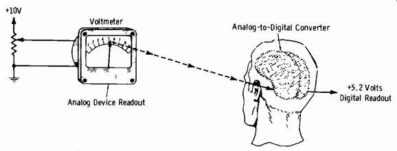
Fig. 3-21. Familiar example of analog-to-digital conversion.
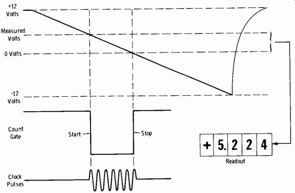
Fig. 3-22. Time-to-voltage conversion for digital voltmeter readout.
One method of obtaining a direct digital readout (digital voltmeter) is illustrated in Fig. 3-22. At the start of the measurement cycle, a ramp-voltage generator is activated. The ramp voltage and the voltage being measured are applied to an input comparator; at the instant these voltages be come equal, a coincidence circuit generates a start pulse which opens a gate. This allows clock pulses to enter a counter. A second comparator circuit senses when the ramp voltage has reached zero. The output of this zero (or ground) comparator generates a stop pulse which closes the gate.
The counter stops, and the resultant count of the clock pulses is displayed on in-line indicating tubes. The accuracy of such time-interval counters can be made extremely good compared to the process of Fig. 3-21. The +5.224-volt indication of the digital voltmeter would be only a guess in the process of Fig. 3-21.
The applications of digital circuitry in broadcasting cover much more than increased accuracy of voltage readings, which is not all that important.
Test generators, audio and rf switching systems, frequency and modulation monitors, and audio tape systems have rapidly become "digitalized." But to keep the subject in focus, we must retain the analog-to-digital and the digital-to-analog relationship, which will be stressed in this Section.
The analog computer is so termed because it can draw an analogy to things in nature. The simple circuit of the voltmeter in Fig. 3-21 can say that the voltage is the force on a body, the resistance is the value of acceleration, and the current is the mass of the body. Since voltage is the product of current and resistance (Ohm's Law) , and force is the product of acceleration and mass ( Newton's law) , the two problems are analogous and can be solved by the same circuit.
The analog computer is a continuous-scale device, able to draw a smooth curve. The digital computer can solve the same problems, but in discrete steps of integers or fractions. The analog computer works with continuous values, whereas the digital computer works with discrete, individual digits.
In fact, the digital device recognizes only two digits, zero and one. From this simple off-on relationship, any numerical value can be "read out."
3-3. THE CONVENTIONAL DECIMAL NUMBER
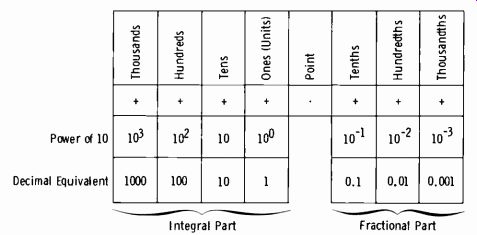
Fig. 3-23. Decimal number system.
The conventional decimal number system is represented by the diagram in Fig. 3-23. The radix is 10. This simply means that digits to the left of the decimal point are integers in powers of ten, and those to the right of the decimal point are fractions in powers of ten.
For example, 3486.412 is read as three thousand four hundred eighty six and four hundred twelve thousandths. It is also 3000+400+80+6+0.4+0.01+0.002.
Or it can be 3(103) +4(102) +8(101) +6(10°) + 4 (10-1) + 1(10-2) + 2(10-3).
In working with the conventional deci mal numbering system, we do not normally convert the numbers in this fashion since it merely complicates an otherwise fast reading. But now we are going to use a numbering system which has only two digits, 0 and 1, which can be used in combinations to represent any number. This is termed the binary system.
3-4. THE BINARY SYSTEM
In the binary system, the radix is 2. All numbers are constructed on the basis of powers of 2. For example, 1001 is 1(23) + 0(22) + 0(21) + 1(2°) .
(NOTE: 2° = 1.) The first term [1(2)) is simply the 1 of the first digit of the number (1001) times 2 raised to the power which represents the number of digits remaining in the original number (3) . To find the decimal equivalent:
1(23)=8
0(22) =0
0(2') =0 1(2°) = 1
Adding: 8 + 0 + 0 + 1 = 9, the decimal equivalent of binary 1001.
Binary Addition From the above, construct the binary table as follows. Start by writing down four zeros:
0000 (Make this equal to zero.)
0001 (Add 1.)
0001
(This equals 1 in the decimal system.) Now add another 1 to get a decimal value of 2.
0001
0001
When 1 is directly under 1 in the binary system, the sum is zero, and 1 is carried to the next column to the left. If there is already a 1 in that column, the sum is again zero and the 1 carries to the left again, etc. So:
0001
0001
0010 (This equals 2 in the decimal system.) Now add another 1:
0010
0001 Add another 1:
0011 (This is 3 in the decimal system.)
0011
0001
0100 (This is 4 in the decimal system.)
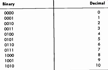
Table 3-2. Binary-Decimal Equivalents (Whole Numbers)

Table 3-3. Binary-Decimal Equivalents (Fractions)
The binary equivalents of the decimal numbers 0 to 10 are given in Table 3-2.
The radix in the binary system is 2 for both whole numbers and fractions. For example, binary 0.010 is 0(2-i) + 1(2-2) +0(2-3) =0+ (1/2)2 + 0 = 0 + 1/4 + 0 = 0.250. Some binary fractions and their decimal equivalents are given in Table 3-3.
It has already been noted that the digits on the left of the binary point are coefficients of increasing positive powers of 2, with 2° adjacent to the binary point. The digits on the right of the point are coefficients of in creasing negative powers of 2, with 2-' adjacent to the point.
For another example, the decimal equivalent of binary 100101.01 is found as follows:
Binary Decimal
1(25) = 32
+0(24) = 0
+0(23) = 0
+1(22) = 4
+0(2') = 0
+1(2°) = 1
+0(2-') = 0
+1(2-2) = 0.25
100101.01 = 37.25
The binary method requires only two digits, 0 and 1. All numbers can be expressed by combinations of these digits. Since it is necessary to work with "powers of two," Table 3-4 is very convenient.
With a number system employing only 0 and 1, an open circuit can signify 0, and a closed circuit can signify 1. So an open switch or relay, a blocked tube or transistor, an extinguished lamp, etc., may represent 0. If the operation is reversed, the device says 1.

Table 3-4. Positive Powers of Two
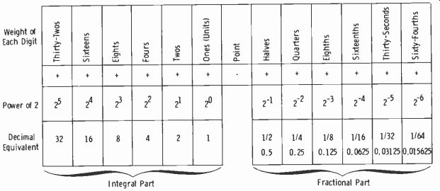
Fig. 3-24. Binary numbers in powers of 2 and decimal equivalents.
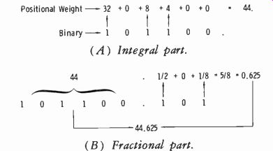
Fig. 3-25. Conversion of binary number to decimal form.
Table 3-2, binary numbers are indicated to four places. Let us see how far we can go with four-place binary numbers in the decimal system.
Starting with 1010 (binary 10) , successively add binary 1 (0001) and obtain 1011 (or 11), 1100 (12), 1101 (13), 1110 (14) and 1111 (15).
Adding 0001 again gives 10000 (binary 16) , which has five places. This tells us that four "gates" (on-off devices) will handle up to the equivalent of 15 in the decimal system.
It is quite easy to convert any binary number to its decimal equivalent if Fig. 3-24 is mentally visualized. Take as an example binary 101100.101, and correlate Fig. 3-25 with Fig. 3-24. In Fig. 3-25A, the positional weights of the digits ( top of Fig. 3-24) are added to obtain 44 for the integral part of the decimal number. In Fig. 3-25B, the fractional part is converted to obtain the total decimal number 44.625 for the 101100.101 binary number.
Complements in Binaries
We are now in a position to study the addition of positive and negative numbers in binary form. For example, consider the addition of 0101 and -0010. Note that in decimal form this is 5- 2. The binary technique is:
change the sign of the negative number, complement this number, and add the result to the positive number.
To complement a binary number, simply change all zeros to ones, change all ones to zeros, and then add one. Thus, to complement 0010:
1101 +1 1110 Then add the 1110 to 0101:
0101 +1110 10011
Now discard the overflow digit in the answer and replace it with either a plus or minus sign. (NOTE: The overflow digit is the digit in the answer one place to the left of the leftmost digit in the two numbers added. In this example, the leftmost 1 in 10011 is the overflow digit.) If the digit is a 1, the sign is plus. If the overflow digit is a zero, the sign is minus. Thus the answer in the example is +0011. This is the binary notation for decimal 3, which satisfies the condition 5-2 = 3.
When a negative number is added to a smaller positive number, the overflow digit is always zero, and the answer is always negative. When the result is negative, the number must be re-complemented to obtain the correct solution. For example: Add -1000 (decimal-8) to 0011 (decimal 3). First find the complement of 1000:
0111 +1
Now add this to 0011:
1000 1000 +0011
01011
Since the overflow digit is 0, discard it and substitute a negative sign, giving -1011. Now re-complement:
0100
+1
0101
So the answer is -0101. This is decimal number-5, which results from adding -8 to +3 in the decimal system.
Binary Subtraction Binary subtraction is exactly the same as addition of positive and negative binary numbers. For example, subtract 0100 (decimal 4) from 1010 (decimal 10) . First find the complement of 0100:
1011 +1
Then add:
1100 1010 + 1100 10110 = +0110
Note that 0110 is decimal 6, which is the result of subtracting decimal 4 from decimal 10.
Binary Multiplication, Digital Methods
Digital computers multiply by over-and-over addition and divide by over-and-over subtraction. A 5-MHz flip-flop can perform five million such operations per second.
Over-and-over addition involves the use of two registers, the accumulator and the multiplier. The accumulator starts with all zeros, and the multiplier keeps account of the number of additions performed. To illustrate, let us start with conventional numbers and multiply 462 x 232:
Accumulator Multiplier
1. 000000 232
2. 000462
3. 000462 231
4. 000462
5. 000924 230
6. 004620
7. 005544 220
8. 004620
9. 010164 210
10. 004620
11. 014784 200
12. 046200
13. 060984 100
14. 046200
15. 107184 (Answer) 000
The above table shows the results of the following operations: In Step 1, zeros are recorded in the accumulator column, and the multiplier (232) is recorded in the right column. In Step 2, the multiplicand is recorded. Step 3 is the first addition, 000 + 462 = 462. Since one addition has now been made, the multiplier is reduced by one, to give 231. In Step 4, the multiplicand is recorded again. In Step 5, 462 + 462 = 924. The multiplier register is again reduced by one to give 230. The first-order digit of the multiplier is now zero, so in the next step, move the multiplicand one place to the left.
(Now the multiplicand will be added ten times in each step.) In Step 7, add Steps 5 and 6 to get 5544, and reduce the multiplier by ten, to give 220. In Step 8, the multiplicand of Step 6 is repeated. In Step 9, the sum of 5544 and 4620 is 10164. Put it down and again reduce the multiplier by ten to get 210. In Step 10, repeat the multiplicand as in Step 8. In Step 11, the total of Steps 9 and 10 is 14784. The multiplier is now 200. Now the second-order digit is zero, so in the next step again move the multiplicand one place to the left. (Now the multiplicand will be added 100 times in each step.) In Step 13, record the new sum in the accumulator column, and reduce the multiplier by 100 to get 100. In Step 14, repeat the same multiplicand. In Step 15, the total is 107184; this is the answer, since the multi plier has been reduced to zero.
Now multiply binary 1011 times binary 11010:
Accumulator Multiplier Operations
1. 000000000 11010 Move multiplicand one place left.
2. 000010110 Add.
3. 000010110 11000
Move multiplicand two places left.
4. 001011000
Add.
5. 001101110 10000
Move multiplicand one place left.
6. 010110000
Add.
7. 100011110 00000
This is the answer.
Converting Decimal Numbers to Binary Numbers
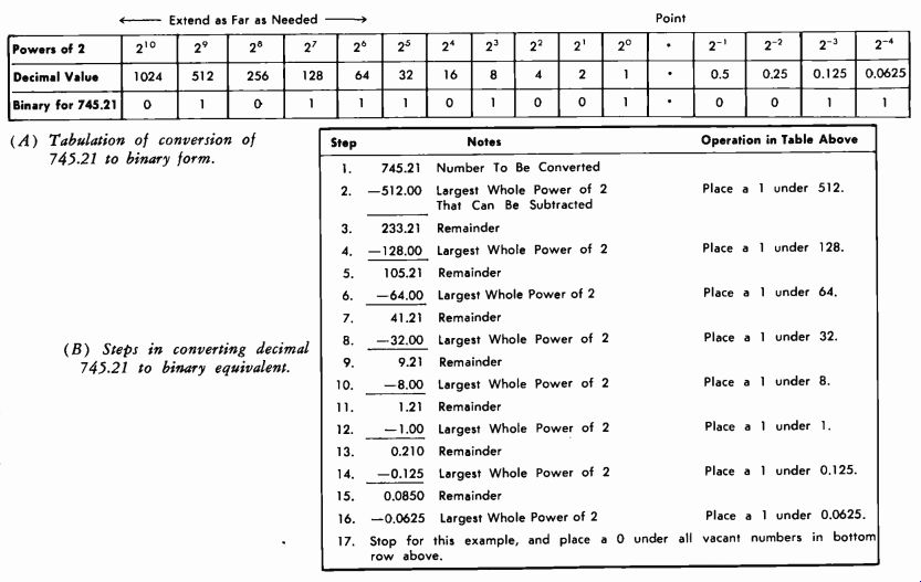
Figs. 3-24 and 3-25 show how easy it is to convert binary numbers to decimal numbers. It is also necessary to be able to convert decimal numbers to binary numbers. In Fig. 3-26A the table of Fig. 3-24 has been extended to a higher decimal value (power of 2) . In the example of Fig. 3-26, deci mal 745.21 is converted to its binary equivalent out to four places to the right of the binary point.
Figs. 3-26
Step 1 (Fig. 3-26B) is to write down the decimal number. Step 2 is to write down the largest whole power of 2 (in decimal value) that can be subtracted from the number. This is 512, so a 1 is placed under the decimal value of 512 in the bottom row of Fig. 5-26A. Step 3 is the remainder, and Step 4 is to find the largest whole power of 2 that can be subtracted from 233.21. This is 128, so a 1 is placed under 128. The process is repeated through all remaining steps. Thus decimal 745.21 = binary 1011101001.- 0011.
3-5. BINARY CODES
Binary numbers can become very long in representing decimal numbers.
In practice, not only numbers but also letters and various symbols are rep resented. For convenience, certain terms are used to identify parts of these binary representations. The term bit means a binary digit (Binary digiT).
The term character means a group of bits. The term word refers to the total number of bits required for a particular system. A word may be defined either by the total number of bits or the total number of characters. For example, a certain system may use a 192-bit word. A character may be divided into (for example) groups of 4 bits. Thus this system may also be defined as using a 48-character word.
Digital systems primarily use instructions in binary form. However, humans use decimal numbers and alphabetic letters. Various codes have been devised to facilitate communication between human operators and digital units.
Pure Binary and BCD Codes
Observe the table of Fig. 3-26A. This shows the pure binary code, which uses the exact positional weight (defined in Fig. 3-24) of each binary digit as the weight value.
See Fig. 3-27. The binary coded decimal (bcd) code employs four binary bits per character and the weight scheme of 8, 4, 2, 1. Each character then has the decimal value that the four bits represent. Note from Fig. 3-27 that the decimal equivalent is simply the binary-number sum expressed in decimal form. Thus 1001= 9, which is 8 + 1.
A 4-bit number can have values from zero to fifteen (0000 to 1111).
Normally, however, only sufficient combinations are used in the bcd code to express all 10 decimal symbols (0 to 9) . To express decimal numbers greater than 9, a separate 4-bit group is used for each digit. For example:
92 = 1001 0010
920 = 1001 0010 0000
591 = 0101 1001 0001
NOTE: A digital system addressed with the 4-bit number using values from 0 to 15 is termed pure binary. When the values used are 0 to 9, it is termed bcd.
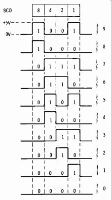
Fig. 3-27. Binary-coded decimal characters.
The USASCII Code
The digital system must be able to work with alphabetic characters as well as numeric characters; this is termed an alphanumeric code. Attempts have been made at standardizing on a universal code. The USASCII ( USA Standard Code for Information Interchange) has been found to be the most widely accepted, although there are many others in everyday use. This code contains seven bits with 128 permutations. The seven bits allow all numerical values plus the alphabet, punctuation marks, symbols and special tele phone and teletypewriter abbreviations to be expressed.
Fig. 3-28 illustrates the entire code. Observe the column headed 100 (column 4) . Capital letters of the alphabet from A to O are listed in order in this column. This information is decoded by using the four digits shown on the left and adding the three digits at the head of the column. For capital A this is:
A = 100 0001
Similarly, for the small letter "a" ( column 6) :
a = 110 0001
The last four binary digits express the decimal number in 8, 4, 2, 1 bcd form. Therefore, the USACII code is compatible with systems designed to use the 8,4,2,1 bcd code.
Octal Coded Binary
The octal system is a common numbering system within the digital area; using it makes it possible to avoid long strings of zeros and ones. The positional weighting is based on powers of eight. The octal system converts readily to binary form and vice versa because the radix of the octal system (8) is an integral power of 2 (8 = 2^3) .
Take the binary word 101001.01, which contains 8 digits. Since the octal system has 23 as the primary base. the word can be arranged in groups of three bits each; this converts to the equivalent octal number. See Fig. 3-29.
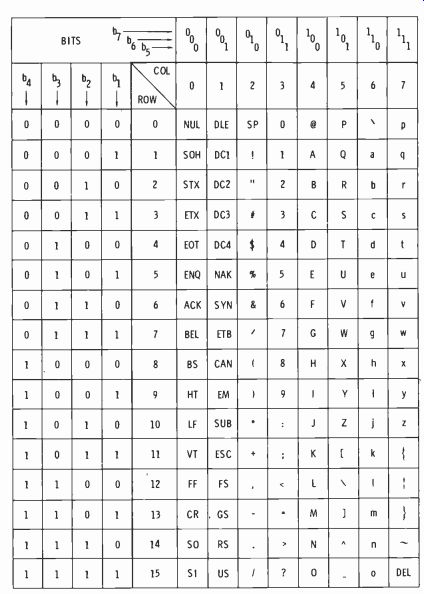
Fig.3-28. USASCII encoding chart.
The word 101001.01 has been arranged in groups of three bits each. Note that when this is done, the corresponding octal digit for each group is determined by the 4, 2, 1 weight factor. Thus the octal number has only 3 digits compared to 8 or 9 binary digits. This is shown by rows A and B of Fig. 3-29.
When converting from octal to decimal form, it is most convenient to use the octal-to-binary conversion as an intermediate step. This is shown by rows B and C of Fig. 3-29. Then the binary number is converted to decimal form in the normal manner as shown by rows C and D.
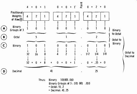
Fig. 3-29. Binary-to-octal-to-decimal conversion.

Fig. 3-30. Basic logic states.
(A) Basic function. (B) Truth table. (C) Diagram symbol.

Fig. 3-31. Fundamentals of an AND circuit.
3-6. BASIC BOOLEAN ALGEBRA
Boolean algebra has become an important link in understanding electronic computer and logic systems. This algebra is concerned with elements that have only two possible stable states and no unstable states. It is useful in representing switching circuits, because a switch can be in only one of two possible stable states, "closed" or "open" (Fig. 3-30) . The symbol 0 (zero) can represent an open switch, and 1 (one) can represent a closed switch. From the outset remember this: The 0 and 1 do not represent numbers; they are shorthand for representing the presence or absence of a conducting path.
0 = Open circuit, or nonconducting path
1 = Closed circuit, or conducting path
Fig. 3-31A shows a simple circuit with two switches in series. Obviously, both switches must be closed to complete the circuit. If either switch A or B is open, the state is O. If both are closed, the state is 1. A truth table for this circuit as shown in Fig. 3-31B; this is a list of all the possible states of the switches ( columns A and B) and the corresponding states of the output function of A and B (in the last column) . Condition 1 is with A and B open (0 state) , so function f (A,B) is also O. Conditions 2 and 3 have only one switch closed (state 1) at a time, so the function of A and B is still O. Condition 4 is with both A and B in the closed (1) state, and therefore f (A,B) = 1. This is an AND (coincidence) circuit. Both A and B must be in the 1 state for a current to exist in the load. The symbol AB is read "A and B." It does not mean the product A X B as in conventional algebra.
Shown in Fig. 3-31C is the diagram symbol for the AND circuit. When this symbol is used without further identification, it should be recognized as an AND circuit. When a regular block is used, it should be labeled AND.
The significance of Fig. 3-32 should now be apparent, except for one thing. The expression A + B is read "A OR B," not "A plus B." This is an OR circuit. The truth table of Fig. 3-32B can be seen to be true if you think of the logic involved. The expression A + B means A OR B, which is function f (A,B) . So if A or B takes the value of 1 (Switched closed) , then f (A,B) must equal 1. Compare this to the logic of the AND circuit (Fig. 3-31)
(A) Basic unction. (B) Truth table. (C) Diagram symbol.

Fig. 3-32. Fundamentals of an OR circuit.
(A) Diagram. ( B) Truth table.
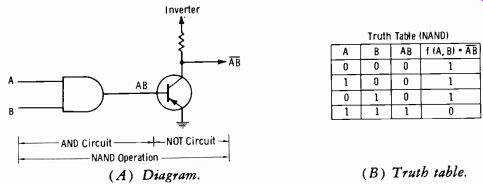
Fig. 3-33. Fundamentals of a NAND circuit.
If 0 is an open circuit and 1 is a closed circuit, what happens when a signal resulting from a given state goes through a phase reversal? See Fig. 3-33A, which shows an AND circuit feeding the base of a transistor. The AND-circuit output is A AND B, so if both inputs are 1's, the base is in a 1 state (condition 4 of the truth table, Fig. 3-31B) . This signal is inverted at the collector, so the output is now a 0 state, or NOT AB, (signified by a line over AB, or AB) . The entire circuit is now termed a NAND circuit.
This simply means the circuit provides an inverted AND, or NOT AND, operation, which is to say an AND circuit with phase reversal.
Note that the first three columns of the NAND truth table (Fig. 3-33B) are a copy of the AND truth table in Fig. 3-31B. But the inverted output changes all 0's to l's, and the 1 to a 0. Note that the whole quantity AB, not the switch is (reversed) .
Fig. 3-34 shows the same kind of logic applied to an OR circuit. When the phase is reversed, the state becomes NOT A OR B (designated A + B) .
Compare the resulting truth table (Fig. 3-34B) with the one in Fig. 3-33B.
For Figs. 3-35 through 3-40, a positive signal is defined as 1. Here is the way to look at these circuits:
Fig. 3-35 shows a diode-logic (DL) circuit. If a positive pulse is applied to either input A or B, A OR B will appear at the output.
Fig. 3-36 is also a diode logic circuit, but in this case the diodes are for ward biased through their respective resistors. If a positive pulse is applied to only one of the inputs, the other diode is still conducting, providing a low-impedance bypass to any signal change. So the voltage at the output remains low. If positive pulses are applied to both inputs simultaneously, the diodes become open switches, and the output rises to the RL supply voltage. This is an AND (coincidence) circuit.
(A) Diagram. ( B ) Truth table.

Fig. 3-34. Fundamentals of a NOR circuit.

Fig. 3-35. Diode-logic OR circuit.

Fig. 3-36. Diode-logic AND circuit.
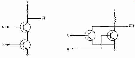
Fig. 3-37. Direct-coupled-transistor; Fig. 3-38. Direct-coupled-transistor logic
NAND circuit. logic NOR circuit.
A direct-coupled-transistor-logic (DCTL) circuit is shown in Fig. 3-37.
A positive pulse applied to only one of the inputs still leaves the other transistor without forward bias. Therefore, the switch is still open, and no change occurs at the output. A positive pulse must be applied to both in puts simultaneously to close the switch. Since phase inversion occurs, the circuit is a NOT AND, or NAND, circuit.
Another DCTL circuit is shown in Fig. 3-38, but in this case a positive pulse appearing at either input will appear inverted at the output. So this is a NOT OR (NOR) circuit. Circuits using only transistors are also termed TTL for transistor-transistor logic.
The diagram in Fig. 3-39 represents a diode-transistor-logic (DTL) circuit. In this case, an OR circuit is followed by a NOT circuit (NOR operation) .
The resistor-transistor-logic (RTL) circuit in Fig. 3-40 is the same as the circuit of Fig. 3-39 except that resistors are used instead of diodes.
Sometimes capacitors are used around the resistors (to enhance switching speed,',. When this is done, the circuit is termed resistor-capacitor-transistor logic ( RCTL) .
Instruction manuals for modern solid-state equipment are filled with the above terminology. Regardless of how complex the circuits may look at first glance. they work on these principles.
3-7. LOGIC-SCHEMATIC NOTATION
You will need to become well acquainted with the term "logic," and know how to read "schematics" of logic systems. It makes no difference in what field you are engaged, electronic equipment is absorbing an ever-in creasing amount of "logic." With such gear, servicing as we have known it will not exist. Some present applications (and a great number of upcoming broadcast and commercial applications) use chips or integrated circuits, (a single chip can replace a fantastic number of transistors) on printed-circuit or etched-wiring boards. Does this mean transistor studies are all in vain, except as a transition from vacuum tubes through transistors to chips? Certainly not.

Fig. 3-39. Diode-transistor-logic; Fig. 3-40. Resistor-transistor-logic NOR
circuit. NOR circuit.
Study and experience with transistors will make the new field of micro miniaturization a "natural." And please rule out any thought that new systems will do away with the maintenance job! The only way this can hap pen is to fail to keep up with the times; and that is nothing new in the technical field. The rate of change in the technology of broadcasting requires technical personnel to spend a greater proportion of time in acquiring new knowledge to solve problems. Continuing education, therefore, is no longer incidental to the job, but an essential part of it.
The digital concept recognizes only two numbers, which are "conditions": 1 and 0. Positive logic means that a 1 (high level) represents the true or more positive level and a 0 (low level) represents the false or less positive level. This is the logic most often used. Negative logic (sometimes used) means that the voltage level assigned to logical 1 is negative with respect to the voltage level assigned to logical 0. Unless stated otherwise, we will be concerned with positive logic in this text.
"Schematics" of logic systems are quite simply block or flow diagrams with certain symbology that tells what is expected of the circuit. It is not possible to service a single "stage" of a microminiature block; you must know how to check for the trouble and then replace a single plug-in "block" on a board, or an entire card of blocks in a multiple-card module.
Fig. 3-41A shows the familiar series of pulses making up a square wave.
Now simply add an L (for low, or negative-going, pulses) or an H (for high, or positive-going, pulses) to each portion of the waveform. Fig. 3-41B lists the nomenclature applied in logic systems. Column 1 indicates a "high-level" or a "low-level" point. Column 2 repeats this in numerical form. Column 3 says the "high" level can be a plus voltage and the "low" level can be ground, or zero volts. Column 4 shows that the high level can be zero volts (common or ground) and the low level can be a minus voltage. In either case, the high level is positive relative to the low level.
Column 5 says that "1" can be "true" and "0" can be "false." This can be reversed, depending upon application. Further columns would be limited only by the imagination; they could be "John" or "Mary," "go" or "no-go," or some other combination.
(A) Pulses. (B) Nomenclature.

Fig. 3-41. Pulse nomenclature for logic systems. (A) Symbol. (B) Waveforms.
(C) Truth table.

Fig. 3-42. Coincidence (AND) gate.
Fig. 3-42A shows the symbol for an AND (coincidence) gate. (Remember that any number of inputs could exist, not just two.) The input wave forms and corresponding output waveform are shown in Fig. 3-42B. Note a significant fact here: When both the A and B inputs are low, the output at C is also low, or zero. But the same output condition exists when inputs A and B have pulses of opposite polarity applied. The significance of this fact is that the coincidence of two positive pulses at the inputs is the "reference" operation; it is the only operation which results in a change of output waveform.
Fig. 3-42C is the corresponding truth table. This table is much more convenient than drawing out waveforms for A, B, and C. Again, it shows that the reference operation (the only condition causing a change in output level) is for two coincident positive pulses (or high, or 1, etc.) to be present at the inputs.
Fig. 3-43A shows the symbol for a NAND gate (NOT AND, or AND gate with inversion) . Note the small circle at the output end of the symbol; this circle indicates signal inversion. From the waveforms of Fig. 3-43B, observe that coincident high-level pulses must occur at the input to change the output to the low level. Note that column C of the truth table of Fig. 3-43C is just opposite to that of Fig. 3-42C.
(A) Symbol.
(B) Waveforms.

Fig. 3-43. NAND gate.
(C) Truth table.
(A) Noninverting stage. (B) High-level activated. (C) Low-level activated.
Leading Edge of Positive Pulse as Trigger Leading Edge of Negative Pulse as Trigger
(D) Triggering waveform.
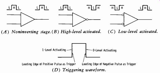
Fig. 3-44. Inversion in logic stages.
(A) Symbol. (B) Waveforms. (C) Truth table.

Fig. 3-45. OR gate with phase inversion.
Fig. 3-44A shows the "triangle" representation of any stage that is non-inverting. (NOTE: In logic circuitry, this symbol is normally replaced by the block symbol of an AND or OR circuit.) In Fig. 3-44B, the circle at the output means that the low-level output is the reference. This symbol rep resents a high-level-activated device, because the high level is required to change the output to a low level. In Fig. 3-44C, the circles are at the inputs.
This is a low-level-activated device; low-level inputs are required for a high-level output.
Fig. 3-44D illustrates that a 1 (high-level) activation is the leading edge of a positive pulse. This is the same as the trailing edge of a negative pulse.
Also, a zero (low-level) activation is the leading edge of a negative pulse.
This is the same as the trailing edge of a positive pulse. These relationships should help to keep the comprehension of "levels" in proper perspective.
Fig. 3-45A shows the most common symbol for the OR gate with phase inversion added; therefore a NOR gate is indicated. The circles at the inputs designate a low-level-activated device; if either input A or B is low, the output will be high. Fig. 3-45B shows the waveforms, and Fig. 3-45C is the more convenient truth table for this circuit function.
Fig. 3-46A shows a block with the labels "SS," "30 µs," "0," and "1." The SS means single-shot (monostable) multivibrator, the 30 µs indicates the unstable (timing) period, and the two outputs (one from each side of the multivibrator) are designated as the 0 output and the 1 output. Some schematics say "OS" (for one-shot) , which is the same as "SS" ( single-shot).
In addition, note that the input line is terminated in a circle. This circle indicates that the input is at low level for the reference polarity of output signals.
( A) Symbol. (B) Waveforms.
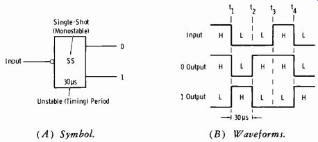
Fig. 3-46. Monostable multivibrator.
Now study the waveforms of Fig. 3-46B. Prior to time t1, the input is high, the 0 output is high, and the 1 output is low. At time t1, the input swings low. This action triggers the single-shot multivibrator into its un stable state (which in this example has a duration of 30 µs); thus the 0 side transfers from high to low, and the 1 side transfers from low to high.
This condition prevails for the built-in timing period of 30 µs, and then at t2 the outputs reverse polarity again. Now remember that the single-shot must wait for another "low" (negative-going) trigger before it can operate again. Thus from t2 to t4 the outputs remain unchanged. At t4, the timing period starts again (negative, or low, input pulse) .
Note carefully that only during the timing period, which was initiated by the negative-going transition, is the 1 output really 1 and the 0 output really zero (or low) . This is the reference pulse mentioned before.
Another basic block of digital circuitry is the flip-flop. This is a bistable multivibrator which remains in its last state until an input causes it to change states. Usually, the input trigger pulse is differentiated and then applied to a diode to polarize the pulse so that only the positive-going or negative-going edge causes the bistable circuit to respond. Sometimes a dc shift rather than a pulse is used.
(A) Symbol. (B) Truth table.

Fig. 3-47. Fundamentals of toggle flip-flop.
(A) Symbol.
(B) Truth table.
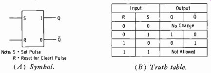
Fig. 3-48. Fundamentals of set-reset flip-flop.
For example, note the symbology for the toggle flip-flop of Fig. 3-47A.
Every time a negative-going edge of a pulse at input T occurs, the bistable changes state. Recall that a multivibrator can have two outputs 180° apart from opposite sides. Thus, if a negative-going trigger arrives when Q=0 and Q=1, then Q flips to 1 and Q to 0.
With the toggle flip-flop, there is no predetermined state for the two outputs when the circuit is first turned on. Thus the state of the outputs following application of a trigger pulse cannot be predicted unless the present state is known. The circuit simply changes states each time a negative-going transition is applied.
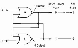
Fig. 3-49. NOR gates cross-connected to form set-reset flip-flop.
The set-reset bistable (Fig. 3-48) overcomes this problem. This circuit (also termed RS flip-flop) has two inputs and the usual two complementary outputs. As indicated by the truth table (Fig. 3-48B) , a 1 input to the set terminal makes the 0 output (Q) a 0 and the 1 output (Q) a 1. A 1 input at the reset (clear) terminal reverses the state: the Q output becomes 0 and the Q output becomes 1. Zero signals on both inputs do not change the state. If both inputs should receive simultaneous signals (l's), the next state cannot be predicted and is ambiguous. Thus simultaneous inputs are commonly termed "not allowed" or "forbidden" combinations. This simply says that the device cannot be in both states simultaneously. The RS flip flop cannot be used in logic situations which include the possibility of simultaneous set and reset inputs.
This is best understood by going momentarily to Fig. 3-49. Two NOR gates cross-connected as shown form a flip-flop. When power is applied, opposite states will exist; we will arbitrarily say these are a 1 output for B and a 0 output for A. The 0 output of A at the input of gate B becomes a 1 at the output, and the 1 output of gate B at the input of gate A becomes a 0 (phase inversion of NOR gate).
(A) Symbol. (B) Truth table.
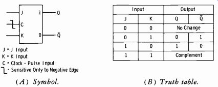
Fig. 3-50. Fundamentals of clocked JK flip-flop.
Now assume a 1 appears at the S (set) terminal. This 1 becomes a 0 at the output of gate B and drives the output of gate A to 1. Thus a set input has set the significant output to the normal 1 and the previous 1 output to 0. A1 input to R will now reset the device to the previous state. Follow this action again from the truth table for Fig. 3-48B. Note .that the circuit is predictable for three of four input conditions.
Flip-flops may be clocked or un-clocked. In the un-clocked flip-flop just discussed, the outputs respond to the inputs as the inputs change. In the clocked flip-flop, a clock input must exist at the time the inputs change for the outputs to respond.
One of the most popular logic elements is the JK flip-flop (Fig. 3-50) .
There are no ambiguous states. When a 1 is applied to the J input, the 1 output (Q) is 1 and the 0 output (Q) is 0. (When the flip-flop is clocked, the clock must be present.) When a 1 is applied to K, the 1 output flips to 0 and the 0 output flips to 1. When a 1 is applied to both the J and K inputs, the flip-flop switches to its complement state. Sometimes two or more J and K inputs exist. One J and one K input may be tied together for use as a clock input.
(A) Wired OR. (B) Exclusive OR. (C) Exclusive OR with (D) Circuit diagram of exclusive phase inversion. OR gate.
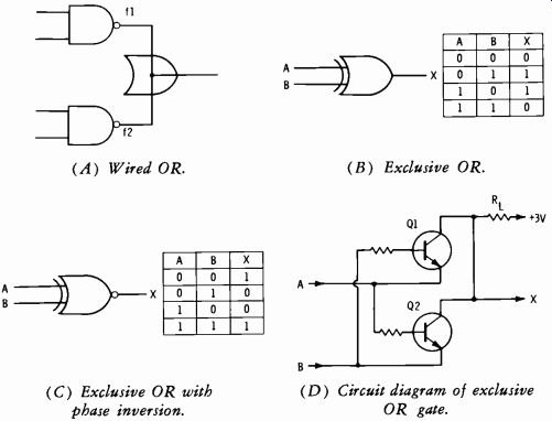
Fig. 3-51. Special forms of gates.
Special forms of gates are used in logic functions, and these gates have special symbols. Fig. 3-51A indicates two NAND gates with outputs paralleled. The symbol indicating that this circuit actually performs as an OR circuit is shown at the junction of outputs fl and f2. This is termed a wired OR or sometimes a phantom OR. The truth statement for this circuit is: If f1 is true OR f2 is true, the output is true.
A circuit which produces a true output only when the input states are not identical is termed an exclusive OR gate (Fig. 3-51B) . Note from the truth table that a 1 (high) output is produced if only one input is 0 (low). If both inputs are of like polarity (either 0's or 1's), the output is 0, or low.
(A) System diagram.
(B) Circuit 1. (C) Circuit 2.
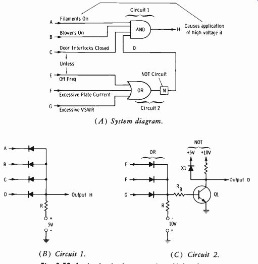
Fig. 3-52. Logic circuits for transmitter high voltage.
The complement of this function is shown in Fig. 3-51C. A 0 output is obtained only if the inputs are of opposite polarity. To make this clear, study the discrete resistor-transistor logic (RTL) circuit illustrated in Fig. 3-51D. If both inputs are 0's or 1's, both transistors have zero-biased base emitter junctions, and neither can conduct. Thus output X sees the full value of supply voltage (high level) since there is no current in R1.
Since the A input is tied to the emitter of Q1 and the base of Q2, and the B input is tied to the emitter of Q2 and the base of Q1, unlike polarity (opposite logic levels) will turn on one of the transistors. The resultant voltage drop across RL will send output X to a low level. Note again that this is the complementary function of the circuit in Fig. 3-51B, as indicated by the small circle at the output of the logic symbol in Fig. 3-51C.
A simple example of how logic schematics are drawn is shown in Fig. 3-52. Output H will apply high voltage to the final transmitter stage if:
Filaments are on Blowers are on Door interlocks are closed but not if:
Exciter is out of frequency limits
Final-stage plate currents are excessive when power is applied VSWR is excessive when power is applied
These conditions mean that output H will be logic 1 when all the inputs (A, B, C, and D) to the AND circuit are logic 1. Inputs A, B, and C are logic 1 if the corresponding conditions are satisfied. The NOT output (which provides input D) will be 1 if inputs E, F, and G are all logic 0.
If any one of these inputs becomes logic 1, the OR output is logic 1. Since this output is complemented ( inverted) by the NOT circuit, output D becomes 0, and high voltage is not applied because output H of the AND gate is logic 0.
Here is a brief review of the action of circuit 1 and circuit 2 in Fig. 3-52: In circuit 1 (AND gate, Fig. 3-52B), if all inputs are at logic 1, the resulting positive potential at the diode cathodes holds the diodes at cutoff, and there is no current through resistor R. Therefore the potential at H is at plus 5 volts, or logic 1. If any one of the inputs goes to logic 0, the associated diode cathode is essentially returned to ground, and the diode conducts. Therefore the voltage at H drops to ground potential (minus the small forward voltage drop across the diode) , and the output voltage be comes essentially 0 ( logic 0) . Thus, all the inputs must be at logic 1 to have logic 1 at the output.
In circuit 2 (Fig. 3-52C), consider the OR gate and NOT gate separately.
If any of the inputs to the OR gate is at logic 1, the associated diode will conduct, and the voltage at the junction of R and RB will be essentially the positive voltage applied to the diode. This back-biases the other diodes, and the oR-gate output goes to logic 1. If all inputs are at logic 0 (ground) , the voltage at the R-RB junction goes to zero minus the small forward voltage drop across the diodes.
Now consider the NOT circuit in Fig. 3-52C. When the base of Q1 goes positive ( indicating a logic 1 from the OR circuit, which in turn indicates a faulty-condition input), the transistor is saturated and output D goes to essentially ground potential. So the AND circuit will not apply high voltage to the transmitter, since input D is at logic 0. When the Q1 base is re turned to ground (all inputs to the OR circuit at logic 0), the transistor is cut off, and output D goes to plus 5 volts, or logic 1. Then if inputs A, B, and C are logic 1, output H causes application of the high voltage.
There is just one thing that might not be apparent immediately; what is the purpose of X1 in the collector circuit of Q1? This diode simply pre vents the logic-1 output from exceeding 5 volts. When Q1 is not conducting, X1 becomes forward biased and clamps the logic-1 output to plus 5 volts. When Q1 is saturated, X1 is reverse biased and effectively out of the circuit. This technique is used when it is desirable to match all input levels to the AND gate.
3-8. THE OPERATIONAL AMPLIFIER
Before taking up the subject of analog-to-digital and digital-to-analog conversions, it is necessary to be familiar with a basic block used in such conversions, the operational amplifier. First study the negative-feedback amplifier of Fig. 3-53. The base-emitter current varies only slightly with relatively large input signal voltages due to the fact that Rin in series with the base is very high relative to the forward base-emitter resistance. Thus the Input source as seen from the transistor base is essentially a constant-current source. The input impedance is essentially the value of Rin, and the transistor base is very near ground potential (about-0.6 volt for a silicon pnp transistor) .
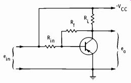
Fig. 3-53. Pnp negative-feedback amplifier.
The ratio of Rf (feedback resistance) to Rin is greater than unity, and for practical purposes the gain (A) of the stage may be considered fixed by this ratio, independent of transistor characteristics. The feedback voltage through Rf is, of course, 180° out of phase with the input voltage and is degenerative. Thus A = Rf/Rin, which simply fixes the ratio of negative-feedback voltage to input voltage. This type of amplifier is sometimes used in computers to multiply the dc input by a constant, which is the fixed stage gain.
An operational amplifier is a direct-coupled (dc) feedback amplifier that has very high gain, high input impedance, and low output impedance.
It normally takes the configuration of Fig. 3-54. It is usually arranged so that the input signal is referenced to ground (Fig. 3-54A) and the output signal is referenced to zero volts dc with respect to ground. The zero dc level at the output is established by operating the amplifier between two power sources of opposite polarity to ground (Fig. 3-54B) , with the output terminal connected to the point which is at zero dc voltage with respect to ground.
(A) Inverting input referenced to ground.
(B) Method of obtaining dc ground at output.
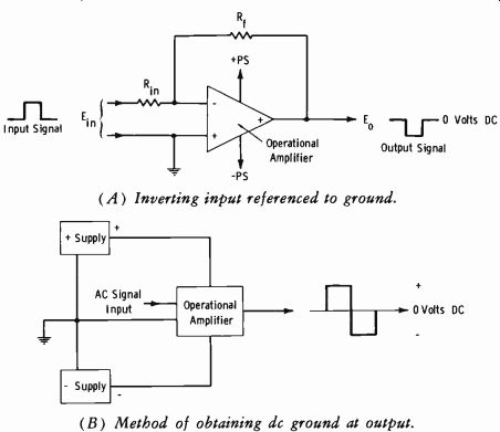
Fig. 3-54. Fundamentals of operational amplifier.
As indicated by Fig. 3-54A, the operational amplifier is represented on schematic diagrams by a triangular symbol with terminals for external connections shown, but no internal details included. The output terminal has a plus sign (when indicated at all) , and one input terminal has a minus sign and the other input terminal a plus sign. The minus input terminal is termed the inverting input (output signal inverted from input polarity), and the plus input terminal is termed the noninverting input (output signal same polarity as input) . With the noninverting input terminal at ground, the no-signal input voltage at the inverting input of the amplifier is at ground dc potential also.
The two inputs of an operational amplifier comprise a differential input.
One input is inverted and the other not inverted. If the same signal is applied to both inputs, the output is E1- E2 = 0. If different signals are applied, the output amplitude is the difference between the input amplitudes; the output depends on actual amplitude difference, width difference, or phase difference. The use of the differential amplifier is covered in applicable portions of following Sections.
At present, we are concerned with the application typified by Fig. 3-54A.
Actual voltage amplification is the ratio of Rf to R,.. Thus:
Rr E =-Et° Rm
NOTE: The negative sign simply indicates that the output is of opposite polarity from the input.
As previously stated, the gain of an operational amplifier is extremely high. When operated as an open loop (no inverse feedback) , it can become merely a switch with (typically) an input signal of only 1 to 5 millivolts.
See Fig. 3-55A. The saturation limits at the ends of the linear transfer curve are termed the common-mode input-voltage limits. ( "Common mode" means one input is at ground or other reference potential, as distinguished from differential input, described earlier.)
(A) Transfer characteristic.
Offset Adjustment
(B) Offset compensation.
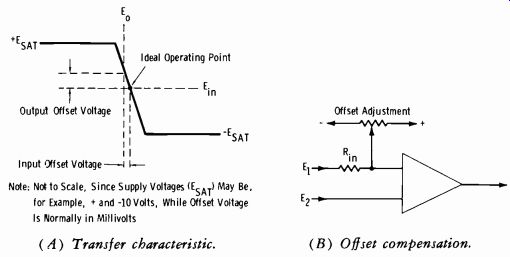
Fig. 3-55. Open-loop operational-amplifier operation.
(When all Rin Are Equal) Fig. 3-56. Voltage summer.
Also indicated in Fig. 3-55A is the "ideal operating point." In the ideal amplifier, the output voltage is zero when the input voltages are zero. In practice, the characteristic is shifted, or offset slightly when the input voltage is zero. Therefore, the technician will normally find an offset-voltage adjustment, as illustrated in Fig. 3-55B. This control is adjusted to balance out the offset.
If a number of voltage sources, E1, E2, E3, etc., are connected through individual resistors of the same value to the inverting input (Fig. 3-56) , the circuit acts as a voltage summer. As stated previously, feedback brings the voltage at the inverting input of the amplifier (point X) to the same level as the noninverting terminal, which in this circuit is ground. Each input signal voltage produces an output the same as if it were the only input present. For example, for E1:
Rr E=-E,- Ri
The total voltage output therefore is the sum:
Eo=-Riñ (E1+E2+E3+...En) R10 need not be the same for all inputs. In that case, the gain for each input voltage is given by the ratio of Rf to the corresponding input resistor.
When the feedback element is changed from a resistance to a capacitance, an integrator or ramp generator is formed. The circuit of Fig. 3-57A is an inverting amplifier with a feedback capacitor Cf, and a switch across the capacitor. In practice, the switch is normally a transistor electronic switching device clocked at a given rate.
(A) Diagram.
(B) Output waveform.
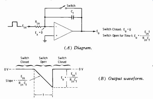
Fig. 3-57. Integrator or ramp generator.
Analyze Fig. 3-57A and 3-57B as follows: When the switch is closed, all feedback current from the output terminal passes into Rin. (For practical analysis, the input impedance of the operational amplifier may be assumed so high that no current enters the amplifier.) The voltage at E. is zero, or the same as the noninverting input, which is at ground. Therefore the output voltage (Eo) is zero because the switch is a direct short between input and output.
When the switch is opened, feedback current from the output terminal must enter the capacitor, and the current through Cf must enter Rin. This degenerative current prevents the amplifier input voltage from changing instantaneously with E_in. The input current and feedback current combine to maintain a constant charging current through Cf, producing a linear voltage change across the capacitor. This is to say that the charging current is constant and is equal to E_in/Ri.
The slope of the output waveform is dependent on time constant Rh, Cf.
Since the input side of the capacitor (Ea) remains at ground potential, the entire voltage change must appear at the side of the capacitor connected to the output terminal. Since E_in is applied to the inverting input, E. must have opposite polarity. Consequently the rate of change (slope) of the output voltage ramp equals- E_in/RinCf.
The voltage across the capacitor is:
...where, E, is the capacitor voltage, t is the time (seconds) the switch is open, Cf is the feedback capacitance in farads, I is the charging current.
It was stated previously that:
Elm I Rin where,
Rim is the input resistance in ohms.
Substituting for I in the equation for E0:
E1t RinCf But:
Therefore:
E, =-Eo
_ Eit RinCf If the input signal ( E_in) is a steady dc voltage while the switch is open, Ea changes at a constant rate of- E_in/RinCf volts per second. The output waveform for a positive input (Fig. 3-57B) therefore is a ramp having a slope equal to this rate. The ramp starts at zero volts and peaks at a value of- E_int/RinCf volts, where t is the length of time the switch is open. The output voltage, of course, levels off if this time is sufficiently long that the amplifier reaches saturation.
It can be seen that the effect of the amplifier is to transform E_in into an output voltage having a rate of change (slope) proportional to E_in with a constant of proportionality of-1/RC. Since this electrical operation is analogous to the mathematical operation called integration, the circuit is sometimes termed an integrator.
3-9. DIGITAL-TO-ANALOG CONVERSION
A common method of converting digital information to analog information involves the use of an operational amplifier with a feedback loop consisting of series-arranged resistors across which are relay contacts or electronic switches. The switches across the individual resistors can be either open or closed, depending on the 0's and l's of the digital data, changing the effective feedback resistance and resulting in an analog output at the amplifier output terminal.
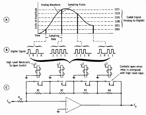
Fig. 3-58. Digital-to-analog conversion using operational amplifier with
variable feedback controlled by relays.
Fig. 3-58A represents an analog waveform which is sampled to result in pulses corresponding to the instantaneous voltage amplitude at the time of sampling. This is termed pulse-code modulation (pcm) . A coding device divides the sampled signals into incremental amplitude levels (right-hand side of Fig. 3-58A) and develops corresponding digital pulses (Fig. 3-58B).
The operational amplifier of Fig. 3-58C contains a feedback loop with a series array of selected resistors, R1 through R4. Each resistor is bypassed with a switch which is open or closed. Although relays are shown for clarity, a transistor switch is often used. If all contacts are closed, the feed-back path has zero resistance (a direct short between output and input) , and no voltage gain is produced (A=Rf/Rio). When a 1 binary input is applied, the switch opens, and resistance is inserted in the feedback path, producing voltage gain. Therefore, E0 represents the analog value of a digital function.
The four bits of each sampling time are fed individually to each of the switches. Take the first sample, 1010. The first 1 (left-most digit) is fed to the first switch; the 0 (second bit) is fed to the switch for R2; the third bit (1) is fed to the switch for R3; and the next 0 is fed to the switch for R4. The process is repeated for the next word. The first bit (left-most digit) is termed the most significant digit, since it has the greatest weighting value (2^3, or 8), whereas the last digit is termed the least significant digit, since 2^0 = 1. The resistance values of R1, R2, R3, and R4 are weighted accordingly to give the correct amount of gain. Note that E,0 can be a reference dc voltage which "traces a curve" at the output in accordance with the initial analog function.
In the example of Fig. 3-58, a four-digit word is used, and four switches are required. A switch is needed for each binary input digit, so a ten-digit word would require ten switches and associated resistors. The greater the number of switches, the smaller the possible incremental difference in output voltage levels can be, and the higher the resolution can be.
Another method of digital-to-analog conversion is a series of transistor switches termed a digilog which feeds a resistance network termed a lad der-adder. The switches simply divide ground between plus and minus reference voltages in the resistor network so that the applied voltages are varied in analog proportion to the digital signals which cause the switching.
3-10. ANALOG-TO-DIGITAL CONVERSION
One type of analog-to-digital conversion was shown in Fig. 3-22, and another type in A and B of Fig. 3-58. In either case, analog inputs are converted, or encoded, into digital outputs. The comparison method is the most common type of analog-to-digital conversion.
The comparison method of converting analog information to digital information is illustrated basically in Fig. 3-59. The familiar sine wave is shown to represent an analog voltage, which may be seen to be analogous to rotation of a potentiometer between plus and minus values through a zero reference voltage. (The input source could just as easily be the secondary of a transformer with the primary connected to a microphone, phono pickup, synchro system, etc.) The potentiometer provides one input to a voltage-comparator circuit. Each position of the potentiometer at any instant is termed the analog address.
The other input to the voltage comparator is a linear ramp voltage from the function generator. The ramp is initiated from a start signal which also enables a gate circuit to allow continuous-running clock pulses to pass to the digital counter (flip-flops) . As long as there is a difference in magnitude between the analog and function-generator inputs to the comparator, clock pulses at a constant repetition rate are permitted to reach the counter.
When the linearly rising ramp voltage reaches equality with the analog address, a stop signal is generated by the comparator; this signal disables the gate and blocks the clock pulses from the counter. The number of pulses accumulated in the counter during the comparison time interval is proportional to the amplitude of the analog input voltage at the time of address, and is the desired digital information.
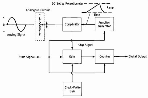
Fig. 3-59. Comparison method of analog-to-digital conversion.
3-11. COUNTERS
A basic block in digital systems is the binary counter, which is simply a series of flip-flops. Although most flip-flops are in the form of ICs, discrete transistors are sometimes used for this circuitry. In any event, it is desirable that the reader have a good comprehension of the action of the binary counter, and this is most readily gained by study of discrete circuitry.
Figs. 3-60A and 3-60B show two identical circuits, not interconnected.
From the base voltage-divider arrangement, it is obvious that each circuit would be conducting. (The base voltage is a little less than 1/2 of the-25-volt supply voltage, in a forward-bias polarity.) Analyze the two extremes of operation as follows.
Saturation: Since the emitter resistance is 1/10 of the collector resistance, the voltage at the emitter would be about -2.5 volts. Since there is negligible voltage drop across the transistor in saturation, the voltage at the collector is also approximately-2.5 volts.
(A) Left half-circuit.
(B) Right half-circuit. (C) complete multivibrator. (D) Use of base supply.
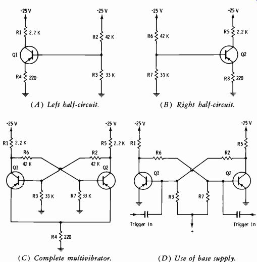
Fig. 3-60. Fundamentals of bistable multivibrator.
Cutoff: Suppose the transistor were driven to cutoff by some means.
Then the collector voltage would be identical to the supply voltage (-25 volts), since there would be no collector current to drop the voltage.
Now suppose it is possible to switch the top end of R2 between the -25 volts and -2.5 volts. Further suppose that the emitter voltage of Q1 can be made a constant-2.5 volts. With this condition, since the base of Q1 will be something under 1/2 of -2.5 volts (actually about -1 volt) , the base is positive relative to the emitter, and the transistor cannot conduct.
Fig. 3-60C shows the individual circuits of Figs. 3-60A and 3-60B cross coupled. The emitters of Q1 and Q2 are now returned to ground through a common resistor, R4. The "top" ends of R2 and R6 are each connected to the collector of the opposite transistor.
For analysis, since both circuits are identical, we must arbitrarily assume one transistor or the other in conduction. Assume Q1 is in saturation. Then its emitter and collector are at-2.5 volts, and the top of R6 is also at -2.5 volts. Note that since the emitters are now common, both emitters will be at -2.5 volts; consequently, Q2 is at cutoff, from the previous analysis.
Since Q2 is cut off, its collector is at -25 volts, the top of R2 is also at -25 volts, and therefore Q1 is truly in saturation. The circuit is "flipped"; in the absence of any change, one transistor is saturated and the other is cut off.
Suppose now that base triggering is used. A trigger applied to either base will start a chain reaction; since pnp transistors are being used, the trigger must be positive to the base of the on transistor, or negative to the base of the off transistor. Assume, for example, that a positive-going trigger is applied to the on transistor, Q1. Transistor Q1 will be driven toward cutoff, its collector will swing negative (less voltage drop across R1), and the base of Q2 will become more negative because of the cross coupling through R6. So Q2 starts to conduct; the drop through R5 swings the Q1 base positive (toward ground from-25 volts), further cutting off Q1.
The regenerative action continues (even though the trigger pulse is very short in duration) until Q1 is completely cut off and Q2 is saturated. The circuit is "flopped"; the reverse conditions from the previous mode now exist. In the absence of any change, the circuit will remain in this mode.
When the bases are returned to ground, a common emitter resistor must be used to make the emitter of the off transistor slightly negative. Thus the less negative base can keep the transistor cut off. The emitter resistor can be deleted when the bases are returned to a slight reverse bias, as shown in Fig. 3-60D. This circuit works the same as that of Fig. 3-60C, except that the off transistor is held off by the external reverse bias.
In the common-emitter circuit of Fig. 3-60C, emitter triggering may be used. When emitter triggering is not used, emitter resistor R4 usually is bypassed with a capacitor to avoid degeneration of the signal voltage.
Further note that in the foregoing example a positive trigger pulse to the base of Q1 was used to turn the transistor off. To turn it on again, a pulse of the opposite polarity would need to be applied to the Q1 base, or a pulse of the same polarity would need to be applied to the Q2 base. But suppose an emitter trigger is used. Assume Q1 is saturated (Q2 off) and the trigger is negative-going. Since the base of Q2 is already positive relative to the emitter, a negative pulse at the emitter will only momentarily increase the reverse bias, and hence will not affect the operation of Q2.
But Q1 is conducting because its base is negative relative to its emitter.
When the negative trigger pulse arrives at the common emitter, Q1 is driven toward cutoff by the reduced forward bias, and regeneration takes care of the rest of the action. Transistor Q1 becomes cut off, and Q2 be comes saturated; the multivibrator has changed state.
Now another negative pulse arrives. Since Q1 is already cut off, it is not affected. But Q2 is driven toward cutoff, and again regeneration causes the circuit to flop back to the original state. So a chain of negative pulses (or, as should be evident, a chain of positive pulses) is all that is required. No "steering" of pulses with regard to polarity is required in emitter triggering. The negative emitter pulse has no affect on the off transistor but affects the on transistor. If the pulses are positive, they will not affect the transistor which is already on, but will affect the off transistor. Remember also that this entire description concerned pnp transistors. For npn transistors, all polarities are reversed. Be sure to visualize the action for npn bistable multivibrators.
(A) Multivibrator with steering diodes.
(B) Steering diodes for (C) Steering diodes for negative pulses. positive pulses.
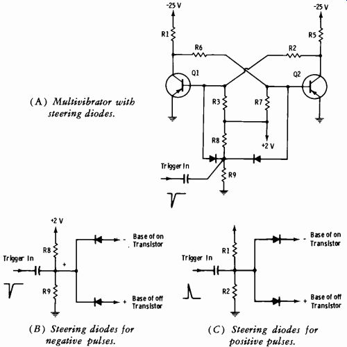
Fig. 3-61. Fundamentals of pulse steering.
Observe again Fig. 3-60D. A trigger at the base of Q1 changes the state of the multivibrator. To change the state again, a trigger of the opposite polarity at the Q1 base would be required, or a trigger of the same polarity at the Q2 base. But we normally will be concerned with a given polarity of trigger pulses for a bistable multivibrator, so let us see how this is done.
See Fig. 3-61A. This bistable multivibrator is identical to the circuit of Fig. 3-60D except for the method of triggering. Negative pulses from one input source are applied to the bases of both transistors. Since this is base triggering for pnp transistors, a negative pulse will drive the off transistor on. See Fig. 3-61B for analysis. Resistors R8 and R9 form a voltage divider from the +2-volt reverse-bias supply so that the cathodes of the diodes are at a slight positive (reverse) potential. The base of whichever transistor is on will be negative, so the corresponding diode is reverse biased, and this circuit remains open (no effect.) The base of the off transistor is held positive by the reverse-bias supply, so its diode is turned "on" by the negative pulse. Hence, the off transistor receives the negative pulse, which turns it on. Regeneration completes the action; the circuit flips and reverses the polarity of the output voltage. The next negative pulse flops the circuit back to the original state. The diodes are termed steering diodes for obvious reasons. Fig. 3-61C shows the diode arrangement for positive pulse steering.
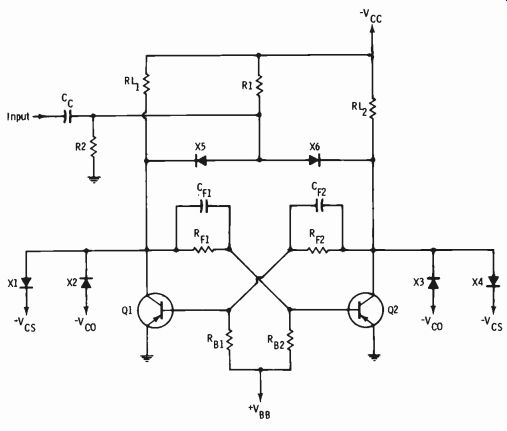
Fig. 3-62. Non-saturating bistable multivibrator.
For analysis of positive-pulse steering, see Fig. 3-61C, and use it in con junction with Fig. 3-62. At the moment, we are confining the analysis of Fig. 3-62 to triggering only (diodes X5 and X6) . This arrangement is always termed collector triggering, but remember that the collector pulse is actually cross-coupled to the opposite transistor base. This cross coupling is what changes the state of the multivibrator.
Since the trigger pulse is positive and the transistors are pnp, the trigger will drive the on transistor off. The steering is evident from Fig. 3-61C when you bear in mind that the base of the on transistor is tied to the collector of the off transistor (Fig. 3-62).
The circuit of Fig. 3-62 is a non-saturating bistable multivibrator. The multivibrator is held out of both saturation and cutoff by means of biased diodes. This decreases the storage time and increases the pulse-repetition-rate capability.
Diodes X1 and X4 with bias source Vcs are used for saturation clamping. Diodes X2 and X3 with bias source Vco are used for cutoff clamping.
The circuit is so designed that without clamping it would both saturate and cut off. Clamping the upper and lower limits of the output permits more reliable substitution of transistors when necessary. The analysis of the circuit is as follows:
Saturation clamping: Collector diodes X1 and X4 have their cathodes returned to a slight negative voltage, for example -2 volts. When the transistor associated with one of the diodes is not in saturation, the anode of the diode is considerably more negative than the cathode, and the diode is effectively an open circuit. When the transistor is driven toward saturation, the voltage at the collector attempts to reach ground potential (more positive than the base) and forward-bias the base-collector junction (the required condition for saturation) . But as soon as the collector reaches a voltage slightly less negative than the diode cathode potential, the diode becomes forward biased, and the collector is held at the Vcs supply voltage.
Thus the transistor cannot saturate.
Cutoff clamping: Diodes X2 and X3 have their anodes returned to a reverse bias which is somewhat less than the collector supply voltage.
When the transistor nears cutoff, the diode is forward biased, and the collector is held at -VVo. This action prevents the transistor from being cut off.
NOTE: Clamping diodes hold the operation in the more linear portion of the output characteristic curve. Thus the average power dissipation is increased, and to avoid transistor damage the designer must choose a load line such that operation of the circuit falls within the maximum permissible power dissipation.
Fig. 3-63 illustrates what a binary circuit does. Note that binary 1 has one output pulse for every two input pulses. Then binary 2 again has one output pulse for every two pulses from binary 1. So the output of binary 2 is at one-fourth of the original frequency. Stated another way:
Total division = 2^n where, n is the number of binary scalers (number of bistable multivibrators or flip-flops) .
A series of binaries can be made to count an odd number, such as the 525 count required in sync generators, by means of reset pulses corresponding to an odd count.
We can now examine in greater detail the readout of a binary counter.
Fig. 3-64 illustrates four flip-flops in cascade, forming a 2^4 = 16 scaler. The capacity of a counter to count to a given numerical value is termed the modulus of the counter.
The series of input pulses (waveform 1 in Fig. 3-64B) is applied to the first flip-flop (FF1), which is assigned the least significant binary number.
The output of FF4 has the most significant (highest order of 2, or 23) binary number. The reader must bear in mind that when we write a binary number, the least significant number is on the right, the reverse of the read out on the block diagram of Fig. 3-64A. In reading the 8-4-2-1 binary output, recall that 2° = 1, 21= 2, 22 = 4, and 23= 8; hence, the binary weight of FF1 is 2°. (Review Fig. 3-24.) The resulting binary count is shown at the bottom of Fig. 3-64 with the digits arranged from the bottom (wave form 5) to the top (waveform 2) so that the most significant number (waveform 5) is in the proper position.
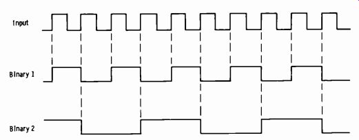
Fig. 3-63. Waveforms of binary circuits.
(A) Block diagram.
(B) Waveforms.
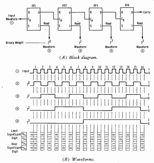
Fig. 3-64. Divide-by-sixteen circuit.
Before analysis of Fig. 3-64, bear in mind the basic facts about a reset-set (RS) flip-flop. When the flip-flop is the set state ( for positive logic) , the 1 side of the circuit reads 1 (high level) and the 0 side reads 0 (low level).
If the circuit is in the reset (clear) position, the 1 side reads 0 and the 0 side reads 1. When the clear (reset) side changes from the 0 state to the 1 state, (1 to 0 on the set side), a pulse is sent to the input of the flip-flop of next higher order, as shown by the block diagram of Fig. 3-64A. Analyze Fig. 3-64 as follows:
Prior to pulse 1: All four flip-flops are in the clear position; thus each output reads 0, and the total counter output is 0000.
Pulse 1: Flip-flop 1 changes to its set position, producing at 1 at its set output. However, neither FF2 nor any of the following stages receives a signal because FF1 produces a pulse at its R (clear) output only when changing from set to reset ( clear) . Note that the counter output is now 0001.
Pulse 2: The second pulse changes FF1 from set to reset, producing a 0 at the set output and a 1 at the clear output. The R output pulse changes FF2 from the clear to the set position ( the S output of FF2 now reads 1) . The clear output of FF2 is 0, and the remaining flip-flops are not affected. Thus the total counter output is now 0010, or binary 2.
Pulse 3: The third pulse changes FF1 to the set state again, but the following flip-flops remain in the previous state. Thus the output is now 0011.
Pulse 4: The fourth pulse changes FF1 and FF2 to the clear position and FF3 to the set position. The output is now 0100.
By continuing this process, the circuit will count up to 15 pulses and then return to clear (0000) on the sixteenth pulse. Table 3-5 shows the resulting truth table for the counter. Note that this analysis has developed a binary-to-decimal conversion table for numbers through the maximum decimal number (15) possible with a four-digit binary.
Thus the highest possible binary number in the output of this counter is 1111, or binary 15. The modulus of any counter is the fixed capacity of the counter plus one. The modulus of this counter then is 15 + 1 = 16.
The addition of another flip-flop would make the modulus 32.
A practical parallel to the above situation can be drawn by considering that most automobiles have odometers with a decimal readout capacity of 99,999.9 miles. Since 99,999.9 is the maximum readout, recycling of the indicator to 00000.0 represents 100,000.0. Thus it is apparent that the modulus of any counter is the fixed capacity of the counter plus one.
There are many varieties of counter, but the technique described above is basic to all types.

Table 3-5. Truth Table for Divide-by-Sixteen Counter
3-12. MEMORY, OR STORAGE
Some instruction guides may refer to a physically separate magnetic tape unit as a storage device and a magnetic-core or drum unit in the same sys-tern as a memory device. Basically, however, the terms memory and storage can be used interchangeably.
A memory unit may consist merely of a series of capacitors that store a charge for a required period of time to be used for readout. Or it may consist of an accumulator which stores data in the form of static dc voltages at the outputs of flip-flop circuits. A memory could store information on a length of magnetic tape or on the magnetic surface of a drum or disc.
Magnetic core matrices are often employed as memories. More recently, integrated-circuit memory devices have become quite common.
A magnetic core is a tiny ring of ferromagnetic material, typically 0.050 inch in outside diameter, 0.030 inch in inside diameter, and 0.015 inch thick. It is capable of retaining saturation in either of two states, depending on the direction of the applied current, which are arbitrarily assigned the values 0 and 1.
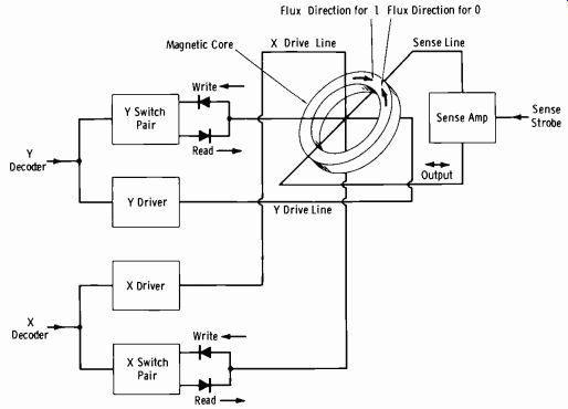
Fig. 3-65. Basic magnetic-core schematic.
See Fig. 3-65. The X and Y drive lines ( explained later) supply the current for core magnetization. A current in one direction establishes a magnetization in the core in a given direction. Reversing the current direction reverses the direction of the flux field and the core magnetization. The write-in and read-out functions determine the current direction as shown in Fig. 3-65.
The X and Y drive lines constitute two separate windings on the core.
To sense the state of a core, a third winding termed the sense winding is used. The two wires (X and Y) are used for write selection, and by reversing the direction of the current, the same two wires are used for read. The write current places the core in a 1 state. The read current shifts the state of the core, and the sense wire picks up the signal voltage generated by the flux change of the core in shifting from 1 to 0. Since the core state stored before sensing is destroyed during readout, this type of memory is referred to as a destructive-readout memory. With this type of memory, if the stored data is to be used again, the readout pulse is immediately followed by a restore (or rewrite) pulse to return the core to the original state.
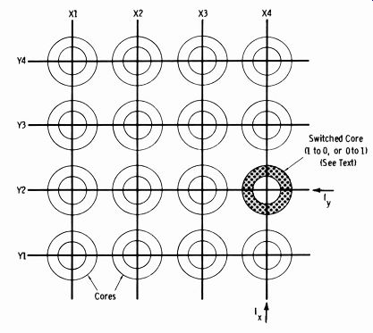
Fig. 3-66. Basic function of magnetic-core array.
A single magnetic core stores one bit of a word. Therefore, core arrays are used; Fig. 3-66 shows a simple 4 X 4 array. The purpose of the "X" and "Y" core winding designations can now be seen. In the example illustrated, simultaneous X and Y currents are being routed only to the core related to X4,Y2 on the rectangular-coordinate matrix. Although the X current is being routed to the other three cores in the X4 line, and the Y current also feeds the other cores on the Y2 line, a single current alone will not change the state of the core. If the X and Y (simultaneous) current applied is a write current and core X4, Y2 is in a 0 state, it is shifted to a 1 state. If the core is already in a 1 state, no change takes place. Then for a read current, the core changes state (1 to 0), and the resultant voltage is picked up by the sense winding. Any core in the matrix is read in a similar manner by application of a read pulse to the associated X and Y winding of the core. If the core has not been switched to a 1 by a previous write current, it contains a 0. Application of a read pulse to the X and Y windings of that core does not switch the direction of magnetic intensity, and no pulse is induced in the sense winding. The read current can only switch a 1 to a 0, not vice versa. Similarly, as previously stated, a write current can only switch a 0 to a 1. If a 1 already exists, no change occurs.
NOTE: In some complex system arrays, a large number of "stacked" arrays are necessary. The X and Y driver windings of each array are in series or parallel with every corresponding X and Y winding on other array assemblies. Some l's and some 0's are normally written in one vertically stacked column of cores. When the X and Y wires are energized to write a 1, the intended cores in the stack must be selected. This is done by running an inhibit wire in parallel with either the X or Y line, adding a fourth winding to the core. A current is made to pass through the inhibit wire in the opposite direction to that in the adjacent (X or Y) drive line. This cancels the magnetic field to prevent writing a 1 into any core that should be a 0.
As previously mentioned, integrated-circuit memories are rapidly appearing in new digital systems. One example is the RCA CD4005 or CD4005D (identical except for physical construction) memory IC. These are 16-word, 1-bit-deep, nondestructive-readout (ndro) memories consisting of 16 flip flop storage cells arranged in an X-Y matrix.
Each storage cell contains a flip-flop which consists of two cross-coupled complementary-symmetry MOS (metal oxide semiconductor) inverter stages and two bidirectional gates. Each gate consists of two n-channel MOS transistors which are connected to perform the gating to and from each cell.
The functional diagram is shown in Fig. 3-67A, and Fig. 3-67B illustrates the cell-arrangement diagram.
Addressing of a particular cell is accomplished by the simultaneous application of high voltage levels on the X-Y coordinates of that cell, just as for the magnetic-core system. A 1 is written into an addressed cell by the application of a low voltage level on the Dl line and a high voltage level on the DO line. Conversely, a 0 is written into the addressed cell by forcing the DO line low and the D1 line high. Nondestructive readout, or sensing, at the Q-sense return line of an addressed cell is accomplished by providing sense current by means of an externally forced high-level voltage on the D1 line. The DO line is also maintained at a high voltage level during readout.
Note: All unused inputs must be connected to the most negative circuit voltage Nssl.
(B) Cell arrangement.
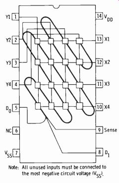
Fig. 3-67. Integrated-circuit memory. Courtesy RCA
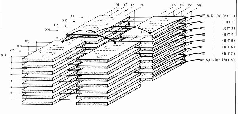
Fig. 3-68. 64-word X 8-bit memory using 32 packages.
Sensing can also be accomplished by external logic-level monitoring of the D1 and D0 lines. In this mode of sensing, logic circuitry that inhibits the writing operation during readout is provided, and the sense line must be connected to Vss (the source voltage supply) .
NOTE: For positive logic, the low level (0) is the negative source voltage, and the high level (1) is the positive drain voltage. Similarly, for voltage sensing, the low level is -1.5 volts, and the high level is -0.9 volt. For current sensing, the low level is essentially zero current, and the high level is 500 p.A.
Expansion of this memory beyond the 16-word, one-bit capacity is accomplished by the utilization of any number of packages. Fig. 3-68 shows how 32 packages can be interconnected to produce a 64-word x 8-bit memory. Word capacity is increased by horizontal expansion in the X and Y directions (increasing the number of cell locations) . The sense lines in each plane (each plane represents one bit) are made common, either by direct connection or through gates. Likewise, the D0 lines are made common and the D1 lines are made common in the same manner. Bit expansion is accomplished by an increase in the number of horizontal planes.
The corresponding X and Y terminals in each plane are connected together (directly or through gating).
As an example of operation, consider writing the 8-bit binary word 10111011 into word location X3,Y4. The least significant bit is bit 1, on the far right (adjacent to the binary point).
1. The X3 and Y4 inputs are set to a high level.
2. The D0 and D1 inputs are set to high (H) and low (L) levels as follows:
Bit Number D0 D1
1 H L 2 H L 3 L H 4 H L 5 H L 6 H L 7 L H 8 H L
To read this same word out of word location X3,Y4:
1. X3 and Y4 are again set to a high level
2. Current from an external source is supplied on the D1 line for each bit (D1 is set to a high level)
3. All DO lines are maintained at a high voltage level All sense leads associated with cells in which a 1 was stored will carry approximately 500 microamperes; those cells containing a 0 will pass virtually zero current through their respective D1 leads.
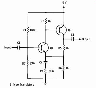
Fig. 3-69. Circuit for question Q3-1.
EXERCISES
Q3-1. Make a dc analysis of the circuit in Fig. 3-69. What voltages would you expect to read at the bases of Q1 and Q2, the collectors of Q1 and Q2, and the emitter of Q1? Assume silicon transistors.
Q3-2. Convert decimal 16 to: (A) pure binary, (B) bcd, (C) octal.
Q3-3. Convert decimal 11 to (A) binary and (B) octal.
Q3-4. Convert decimal 568 to (A) binary and (B) octal.
Q3-5. Convert binary 101001.01 to decimal.
Q3-6. Read aloud the expressions: (A) AB, (B) A + B.
Q3-7. Define the terms: (A) DTL, (B) RTL, (C) RCTL, (D) TTL.
Q3-8. Prepare the truth table for circuit 1 (AND) of Fig. 3-52A.
Q3-9. Prepare the truth table for the OR portion of circuit 2, Fig. 3-52A.
Q3-10. Prepare the truth table for the NOT portion of Fig. 3-52A.
Q3-11. Does a series of cascaded binaries always count to 2n, where n is the number of binary circuits?