In commercial receivers, we find circuits in which the sync pulses are separated from the composite video signal by clippers.
Processing circuitry develops sync waveforms of suitable polarity, separates the vertical sync pulses from the horizontal sync pulses, clips and levels the pulse trains, and provides either single- or double-ended output as required by subsequent receiver circuits. Sync takeoff may be made either in the video detector or video-amplifier section.
A sample of the composite video signal is fed to a clipper circuit, as shown in Fig. 10-1. Either a diode or a transistor may be used as a clipping device. The advantage of a transistor is its amplification of the clipped pulses. In Fig. 10-1A, the incoming composite video signal is coupled to the diode circuit via capacitor C. This coupling capacitor removes the dc component from the composite video signal and also provides signal-developed bias across the diode.
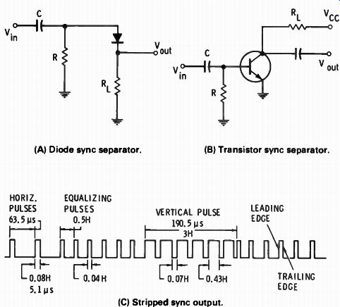
Fig. 10-1. Either a diode or a transistor may be used as a sync separator.
(A) Diode sync separator. (B) Transistor sync separator. (C) Stripped sync output
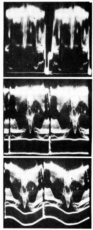
Fig. 10-2.
Normal proportions of sync-pulse and camera signal amplitudes.
(A) 7875 Hz deflection (B) 30 Hz deflection. (C) Composite video signal with excessive 60 Hz hum.
Signal-developed bias provides the best separating action when the incoming signal amplitude varies or when hum voltage is mixed with the composite video signal, as shown in Fig. 10-2C. The clipping level in the waveform is automatically maintained because the value of the signal-developed bias is proportional to the amplitude of the applied signal. Note, also, that coupling capacitor C has comparatively great reactance at 60 Hz and tends to suppress hum voltage.
Signal-developed bias is produced in Fig. 10-1A as follows: Positive portions of the applied waveform cause diode conduction, and negative portions are blocked by the back resistance of the diode. Forward current flow through the diode develops a negative charge on the right-hand plate of capacitor C. In turn, the diode becomes reverse-biased as a voltage that depends on the amplitude of the positive excursion of the video signal.
Between sync pulses, the charge on C decays at a rate that depends on the RC time constant of the circuit. When R and C have correct values, clipping occurs at the black level in the composite video signal. Clipping action is checked to best advantage with a oscilloscope. An oscilloscope-control familiarization diagram is shown in Fig. 10-3.
Transistors are also used to perform much the same functions.
Figure 10-4 shows a typical transistor-limiter configuration. The collector-current waveform is limited because the base-drive voltage swings the base past the cutoff point. An example of saturation limiting is seen in Fig. 10-5. The collector-current waveform is limited because the base-drive voltage swings the base past the saturation point. Note that when a transistor is saturated, the collector-current flow is so heavy that the voltage drop across the collector-load resistor brings the collector voltage down to a very low value.
Conversely, transistors are employed to obtain clipping action.
Figure 10-6 depicts a negative-peak clipper. The input signal causes the base to draw current on negative half-cycles. In turn, the coupling capacitor is charged and applies a positive signal developed bias voltage on the base. Then the transistor is reverse biased in the presence of a signal. Between successive signal peaks, some of the bias voltage leaks to ground. Therefore, the peaks of the applied waveform are clipped, and appear in the output circuit.
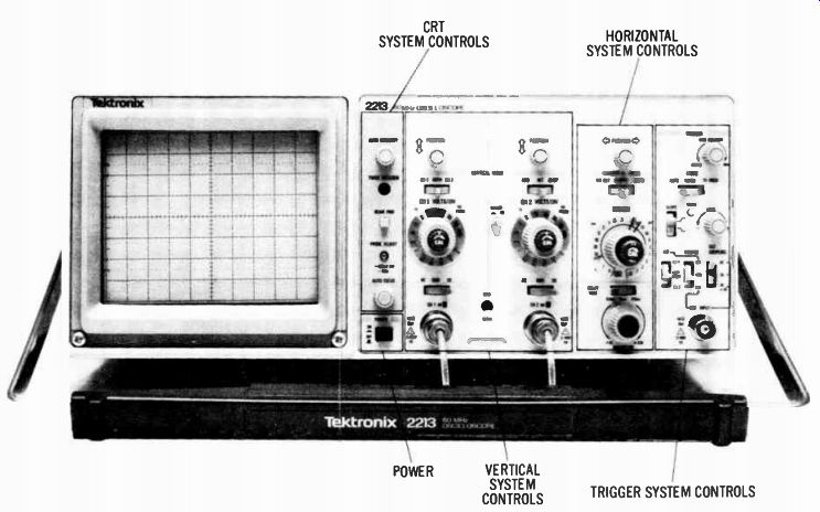
Fig. 10-3 . Oscilloscope-control familiarization
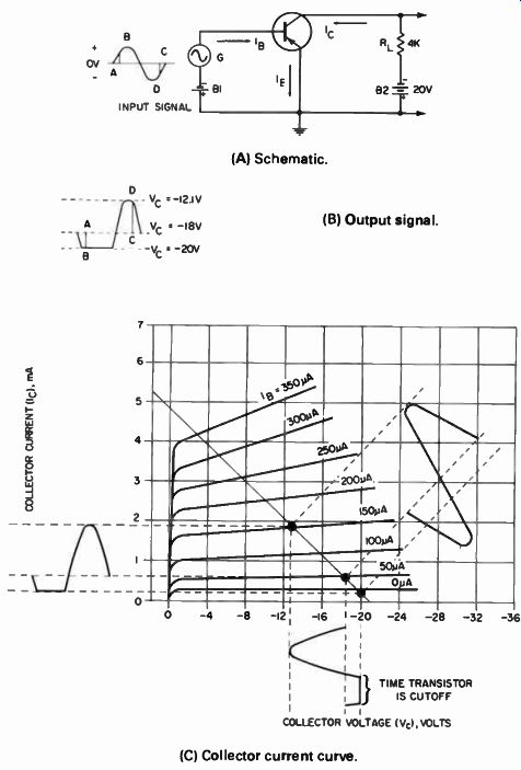
Fig. 10-4. Cutoff using PNP transistor.
(A) Schematic. (B) Output signal (C) Collector current curve.
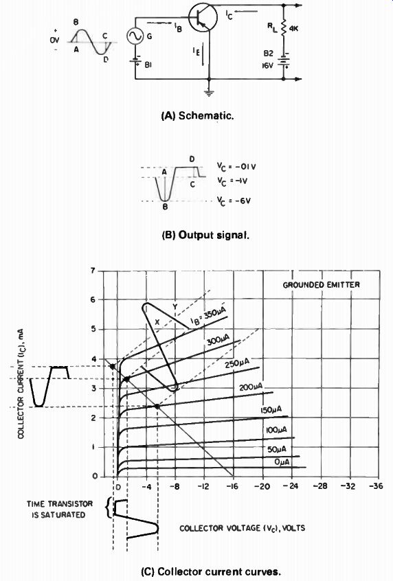
Fig. 10-5. Saturation limiting using PNP transistor.
(A) Schematic. (B) Output signal (C) Collector current curves.
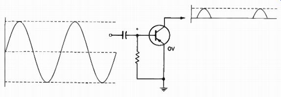
Fig. 10-6. Negative-peak clipper.
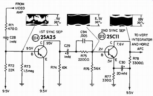
Fig. 10-7. Typical transistor sync-separator configuration.
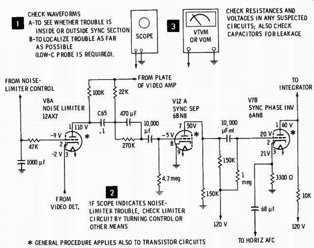
Fig. 10-8.
Many transistor TV receivers employ at least two sync separator stages. Each stage operates as a clipper: The first stage clips off the top portion of the waveform, and the second stage clips off the bottom portion of the waveform. Note that the first transistor inverts the waveform polarity, thus providing for bottom-clipping. Q14 operates chiefly as a saturation clipper.
In the second stage of Fig. 10-7, Q15 is biased 0.3 volt beyond cutoff by signal-developed bias in normal operation. Accordingly, the first 0.3 volt of the sync tips becomes clipped. Q15 is also driven into collector saturation and thereby clips any residual video signal. The coupling capacitors tend to differentiate the sync waveform; therefore, C94 and R75 are included to provide integrating action that tends to restore the normal waveshape.
Another circuit action provided by C94 and R75 is due to the impedance that they provide between the collector of Q14 and the base of Q15. This impedance prevents overdriving of Q15 on strong signals, which would result in excessive increase of pulse width at the collector of Q15.
A preliminary analysis of trouble symptoms in the sync section is shown in Fig. 10-8.
SORTING INDIVIDUAL HORIZONTAL AND VERTICAL PULSES
In our foregoing description of various methods of separating synchronizing pulses from the composite video signal, only the narrow horizontal pulses were mentioned. The longer vertical pulses are clipped from the signal in the same separation process.
After the sync pulses have been removed from the video signal, the vertical pulses must be sorted from the horizontal pulses, and each one must be fed to its respective deflection-scanning system. Since the horizontal and vertical pulses are equal in amplitude, the methods of separation for clipping them from the video signal cannot be used to distinguish between them. They do, however, differ in time duration; and on this basis sorting is accomplished.
We shall now consider the action of such systems as differentiating networks for removing horizontal pulses and integrating networks for the vertical-pulse acceptance.
Horizontal-Pulse Separation
Horizontal pulses of the transmitted signal are approximately 5¡sec in duration. These pulses are impressed on a circuit of the type shown in Fig. 10-9C, which is known as an RC differentiating circuit.
Differentiation means the breaking down of a quantity into a number of small parts. The pulses in Fig. 10-9A are made into smaller parts, as shown in Fig. 10-9B by the action of the circuit in Fig. 10-9C. The circuit consists of a capacitive and resistive combination in which the capacitor is in series with the separated pulse input and the resistor is shunted across the output. The time constant of this circuit is made short compared with the duration of a horizontal-sync pulse. The sync pulse is held between 4 and 5 sec, and the time constant of the horizontal differentiating circuit is made between 1 and 2 µsec. In an RC circuit in which the time constant is short compared with the duration of the applied square-wave pulse, the capacitor is completely discharged between pulses.
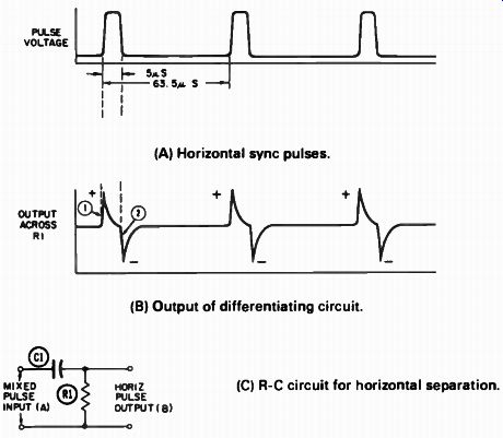
Fig. 10-9. Horizontal-pulse separation, or differentiation.
(A) Horizontal sync pulses (B) Output of differentiating circuit. (C) R-C circuit for horizontal separation.
A sharp pip of voltage occurs across the resistor at both the leading and trailing edges of the applied square-wave pulse. The amplitude of the pip is determined, not only by the amplitude of the square wave, but also by the steepness of the edge of the square wave. For this reason, the FCC limits the allowable slope of the leading and trailing edges. These slopes must not occupy more than 0.4 percent of the horizontal-line scanning interval of 63.5 µsec.
The voltage pip due to the leading edge of the horizontal synchronizing square wave is shown as a positive pip at 0 in Fig. 10-10B. The dip due to the trailing edge of the horizontal pulse is shown as a negative voltage at . The leading-edge pulses control the horizontal-scanning oscillator. The negative pulses are rejected by cutoff or saturation of one or more stages of the sync system.
When the longer-duration, vertical-synchronizing pulses arrive, the differentiating circuit acts as shown in Fig. 10-10B. Here, again, a positive pip occurs at the leading edge of each vertical pulse, and a negative pip occurs at the trailing edge. The leading edge pulses continue to control the horizontal oscillator during vertical retrace. In this instance, however, two pulses occur during a horizontal-line scanning interval. Only the first of these pulses is used to control the horizontal oscillator; the second pulse cannot cause lock-in since it occurs while the oscillator is insensitive to tripping.
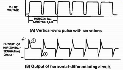
Fig. 10-10. Action of horizontal-differentiating circuit on vertical-sync
signal.
(A) Vertical-sync pulse with serrations. (B) Output of horizontal-differentiating circuit.
The horizontal pulses can be separated by other means than the RC differentiating circuit just described. Figure 10-11 shows two types of differentiating circuits that employ inductance and a third type that uses the properties of a resonant circuit.
The inductance of the circuit in Fig. 10-11A is connected in series with the plate circuit of a tube that has been biased to clip the sync pulses from the video signal. The waveform of the sync pulse plate current consists of steep slopes, which correspond to very rapid changes of current. The voltage across the inductance is proportional to the rate of change of the current through it.
Thus, at the leading and trailing edges of each current pulse, a high voltage is produced across the inductor. This voltage is the same form shown for the RC type of differentiator (Fig. 10-9B). If the pulses are of proper polarity and sufficient amplitude, they can be applied directly to the scanning generator by a capacitor connected to the plate end of the inductor. If the polarity is incorrect, phase reversal can be accomplished by an amplifier stage or by a transformer, as shown in Fig. 10-11B. When a transformer is used, secondary L2 me be connected so that the output-voltage pulses have opposite polarity to those across primary L1. The secondary can be connected directly to the input circuit of the horizontal-scanning generator.
The circuit shown in Fig. 10-11C operates quite differently from the two circuits just described. The resonant circuit, consisting of L1 and C1, is tuned to approximately seven times the horizontal-line frequency of 15,750 hertz, or 110 kHz. The separated sync pulses are impressed across the circuit and shock-excite it into oscillation at its resonant frequency. The oscillation is quickly damped out by parallel resistor R 1. Only the first half cycle of voltage across the circuit is used to control the horizontal-scanning oscillator, corresponding to a pulse duration of approximately 5 µsec.
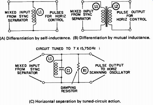
Fig. 10-11. Other methods of horizontal-sync-pulse separation.
(A) Differentiation by self-inductance.
(B) Differentiation by mutual inductance.
(C) Horizontal separation by tuned-circuit action.
Several advantages can be cited for this method of horizontal sync discrimination:
1. An extremely simple pulse-separation and oscillator-control system can be used. The circuit can be connected directly in the plate return of the sync-separator tube and coupled directly to the scanning oscillator because pulse shaping is performed by the resonant action.
2. This method is relatively immune to excitation by static or ignition noise because such pulses would have to be of the proper time duration (5 µsec) and repetition rate (15,750 hertz) to produce ringing; the probability of such coincidence is slight.
Vertical-Pulse Separation
In the description of vertical-scanning systems, we mentioned integrating networks for segregating the long-time, vertical-field pulses from the sharp, horizontal-line pulses. We shall now consider the means of sorting these vertical-field scanning pulses from the composite scanning pulses and of using them to control the vertical-oscillator timing.
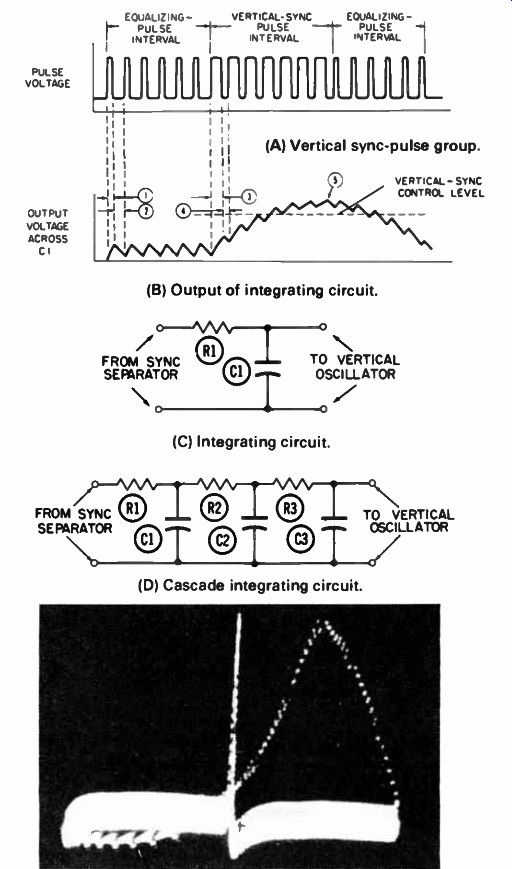
Fig. 10-12. Vertical-pulse separation by integration.
(B) Output
Output of integrating circuit.
(A) Vertical sync-pulse group.
(C) Integrating circuit.
(D) Cascade integrating circuit
The integrating action that sorts the vertical pulses from the complex video signal is exactly opposite from the differentiation process for separating the horizontal pulses. Integration means the addition of a number of small elements to form a whole. Fig. 10-12C shows an integrating circuit; it is the opposite of the differentiation circuit shown in Fig. 10-9. The resistor is in series with the input, and the capacitor is connected across the output.
The time constant of the combination is much longer than that employed for sorting the horizontal pulses. This time constant is made approximately equal to the duration of a horizontal pulse.
Consequently, the charge accumulated by the capacitor because of the horizontal pulse is small and will decay rapidly.
This action is shown in Fig. 10-12B. During the time shown at 0 , the equalizing pulses produce only a small voltage across the capacitor. This voltage decays to near zero in the interval between pulses, as shown at 0 . The much longer vertical synchronizing pulses produce a greater charge in the capacitor during period 0 . This charge does not completely decay during the short serration interval 0 . Consequently, each vertical pulse adds an element of charge to the capacitor, and the voltage continues to build up during the interval of vertical pulses. The dotted line in Fig. 10-12B indicates the level at which the voltage becomes large enough to trigger the vertical-scanning oscillator.
This point usually occurs after two or three vertical pulses have charged the capacitor.
The vertical-integrating network is seldom the two-element type as shown in Fig. 10-12C; it is usually a cascade network, as shown in Fig. 10-12D. The resultant time constant of this network is smaller than that of any of the individual branches (R1-C1, R2-C2, or R3-C3). The overall time-constant calculation is the same as for resistors in parallel. For the three-branch circuit in Fig. 10-12D, with Ti for the time constant R1 X C1, T2 for R2 x C2, and T3 for R3 x C3, the effective circuit time constant T will be:
1 1+- 1+ 1 ==-- T T, T 2
Individual time constants for a three-branch circuit in a modern receiver are 30 to 60 µsec. The effective overall circuit time constants, therefore, are between 10 and 20 u.sec.
The reasons for using cascaded integrating circuits are:
1. To prevent erratic control of vertical retrace by random noise or static pulses. Before such pulses could control the vertical oscillator, they would have to be more comparable in duration and spacing to the vertical-sync pulses.
2. To smooth out the contour of the rising voltage wave (shown in the interval 3 to 5 of Fig. 10-12D) across the output capacitor. The action is similar to that of the familiar resistance-capacitance, power-supply filter system in which the ripple is reduced by successive stages.
Because of this smoothing action, an individual horizontal pulse cannot cause pairing of lines during retrace. The sections of the cascade network are usually not made with equal time constants. This unbalance prevents accidental triggering by noise pulses.
FUNCTION OF VERTICAL-EQUALIZING PULSES
In Section 1 we briefly discussed interlaced scanning, which prevents flicker of the image. For simplicity, the retrace from bottom to top of the picture was shown as a straight line, or single jump. Actually, the horizontal oscillator must be kept in step with the transmitter during vertical retrace, which lasts from 1250 to 1400 µsec (20 to 22 horizontal lines). Figure 10-13 shows a simplified version of the downward scanning, in which 9 V2 lines have been drawn to represent each field. Actually, a field consists of 262 1/2 lines minus the lines lost during retrace.
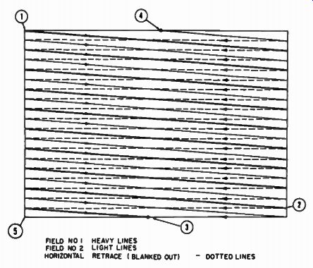
Fig. 10-13. Active downward fields.
The first field, which starts at the upper-left-hand corner O and ends at the bottom center of the picture 0 , is shown by heavy lines. The second, or interlaced, field starts at the top center 0 and ends at the lower-left-hand corner ; it is shown by light lines. During vertical retrace, when the picture is blanked out, the beam moves upward under the combined action of both the vertical- and horizontal-deflection systems. This is represented in simplified form by the diagram in Fig. 10-14. Here, 3 lines represent the 20 to 22 lines actually required during vertical retrace; again, a heavy dotted line represents the retrace of field No. 1, and a light dotted line represents the retrace of field No. 2.
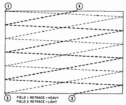
Fig. 10-14. Inactive upward fields (vertical retrace).

Fig. 10-15. Vertical-sync signal for retrace after field 1.

Fig. 10-16. Vertical-sync signal for retrace after field 2.
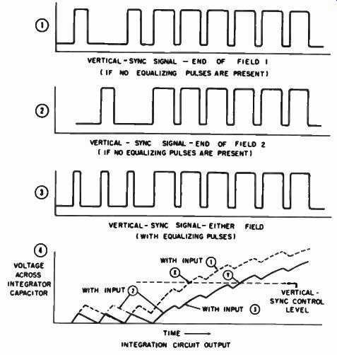
Fig. 10-17. Action of vertical-integrating circuit for successive fields (with
and without equalizing pulses).
The dual functions of producing vertical retrace at the proper instant and keeping the horizontal oscillator in synchronism are controlled by the equalizing and vertical pulses shown in Figs. 10-15 and 10-16. The vertical-sync signal for the retrace of field No. 1 differs from that of field No. 2 by the spacing between the last horizontal pulse and the first equalizing pulse. In Fig. 10-15, for field No. 1, this space "a" consists of only one-half of a horizontal line since field No. 1 ends at the middle of the last line, as shown at 0 of Fig. 10-13. In Fig. 10-16, for field No. 2, the space "h" between the last horizontal pulse and the first equalizing pulse consists of an entire horizontal line. Vertical blanking starts at the leading edge of the equalizing pulses. Thus, the successive field-blanking time is accurately set up by the signal.
Even though retrace blanking is accurately established, vertical retrace may not take place at the proper instant unless the critical charge on the integrating capacitor occurs at exactly the same point for each successive vertical-sync signal. How the equalizing pulses ensure this condition is shown in Fig. 10-17. At 0 is shown the composition of a vertical-sync signal that would follow field No. 1 if the equalizing pulses were not present. This signal input to the integrating circuit would charge the capacitor, as shown by dotted line 0 on the charge curves of Fig. 10-17.
This curve crosses the sync-control level at time X. The vertical signal, without equalizing pulses, for retrace at the end of field No. 2, would be as shown at ® in Fig. 10-17. On the charge curves, the critical sync-control level would be reached at time Y, which is so much later than time X that proper interlace would not occur. When equalizing pulses are employed as shown at 4 3 , the critical firing point for the vertical oscillator is at time Y for both fields. Successive fields preceded by equalizing pulses will therefore accurately control the oscillator and ensure proper interlace.
ACTION OF HORIZONTAL-DIFFERENTIATING CIRCUIT DURIN G VERTI CAL PULSE
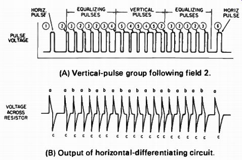
Fig. 10-18. Action of horizontal differentiating circuit during vertical-pulse
period. (A) Vertical-pulse group following field 2. (B) Output of horizontal-differentiating
circuit
The formation of positive and negative pips at the leading and trailing edges, respectively, of the vertical-sync pulses was de scribed briefly. We shall now consider in detail the action of the horizontal-differentiating circuit during the entire vertical pulse.
Figure 10-18 shows the pattern of the vertical signal following field No. 2.
The horizontal pulse, which starts retrace of the bottom line of the picture, is shown at 0 in Fig. 10-18A. The positive-output pip produced by its leading edge is shown at "a" in Fig. 10-18.
The pips produced by the trailing edge of this horizontal pulse and all the other pulses of the period (labeled "c") are rejected by the sync system, as previously explained.
Each equalizing pulse @ and 0 before and after the vertical pulse also produces a pair of positive and negative pips. Only the pips marked "a" are used for oscillator control; those labeled "b" are rejected since they occur in the scanning cycle while the horizontal oscillator is not sensitive to pulse control.
Each pulse of the vertical group 0 and 0 also produces a pair of positive and negative pips. However, only the positive pips "a" of Fig. 10-18B are used. The horizontal pulse shown at 0 is one of a group occurring during the blanking period. The pips produced by the pulse at 0 are the same as those produced by horizontal pulse 0 . It is evident that the vertical-pulse group, because of the individual pulses and their different lengths, can ensure vertical retrace at the proper time and keep the horizontal oscillator in step with the scanning in the camera tube at the transmitter.
AGC CIRCUITS
Automatic gain control (AGC) minimizes the effect of changes in signal strength at the receiver antenna. The gains of the RF and IF stages are so regulated that a strong signal is amplified less than a weak signal. As a result, the quality of the TV picture tends to be relatively constant.
Variations in signal strength are of two types: (1) variations between signals received on different channels; and (2) variations occurring from time to time on the same channel.
Both strong and weak channels are available in many locations.
If AGC is provided in the receiver, the contrast control does not need to be reset each time a new channel is tuned in. AGC also compensates for extremely strong signals received in powerful station areas.
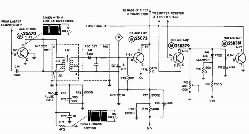
Fig. 10-19. Transistor keyed-AGC system.
The AGC system levels out most of the periodic amplitude variations that would cause fading on a particular channel; there fore, a steady picture is obtained even in moderate fringe areas.
The rapid flutter caused by airplanes flying near the path of the transmitted signal is also corrected as much as possible through AGC action.
A transistor keyed-AGC system is depicted in Fig. 10-19. Four de amplifier stages and an AGC-IF amplifier stage are used. The IF signal from the last IF transformer is applied to the base of transistor Q6, which operates as a keyed amplifier. A 20-volt, peak-to-peak pulse is applied via gating diode X40 to the collector of Q6. In turn, amplified IF bursts are fed to the AGC detector X41. The burst waveform is depicted in Fig. 10-20. The rectified and filtered de output is stepped up through Q7 and is then applied to the base of the first IF transistor.

Fig. 10-20. Output from Q6 in Fig. 10-15-a train of pulsed bursts.
Thus, the AGC current is amplified by the first IF stage and fed to the base of transistor Q8 in Fig. 10-19. This is a common emitter de amplifier, which supplies output to the AGC delay diode X42 and to the base of Q9. In turn, the delayed AGC current is amplified by Q9 and then applied to the RF amplifier stage. The delay threshold is set by R12 in Fig. 10-19.
We recognize that the transistor AGC system is basically similar to a tube-type amplifier AGC system, except that control current is processed instead of the control voltage. Another difference to be noted in Fig. 10-19 is that part of the de amplification is provided by the first stage in the IF strip.
The delay circuit holds the AGC bias applied to the RF amplifier to about zero until the incoming signal is strong enough to develop -4 volts of bias in the IF section of the AGC line. The RF bias appears at this signal level, increases more rapidly, and eventually becomes greater than the IF bias. When the incoming signal is strongest, the RF amplifier is biased most heavily, and the signal is promptly reduced before it has a chance to overload any of the IF amplifiers.
Various types of AGC arrangements are found in transistor TV receivers. These may be classified as follows:
1. Un-keyed reverse AGC
2. Keyed reverse AGC
3. Un-keyed forward AGC
4. Keyed forward AGC
5. Amplified AGC (used with any of the foregoing arrangements)
Reverse AGC action is obtained by reducing the base-emitter bias on a transistor. As the cutoff point is approached, the gain of the transistor decreases rapidly. Forward AGC action is obtained by reducing the collector voltage on a transistor by inserting substantial series resistance in the collector circuit. When the AGC bias causes the emitter to draw more current, there is a greater voltage drop across the collector resistance, and the collector voltage decreases. As the saturation point is approached, the gain of the transistors decreases to a small value. Mesa transistors provide better AGC control action with reverse AGC; on the other hand, MADT transistors proved better AGC control action with forward AGC.

Fig. 10-21. AGC takeoff from secondary of last IF transformer.

Fig. 10-22. Single diode may operate as both a video detector and an AGC detector.
In a simple un-keyed-AGC system, a separate AGC detector may be used, as shown in Fig. 10-21, or a single diode may operate as both a video and an AGC detector (Fig. 10-22). To obtain a wide control range, this system must be followed by an AGC amplifier. We shall find that an IF transistor may do double duty as a common-emitter, IF-signal amplifier, and as a common-collector, de amplifier for the AGC system. In any case, we usually find a supplementary AGC amplifier employed, as depicted in Fig. 10-23. A common-emitter de amplifier is followed by an emitter-follower amplifier. The emitter follower matches the comparatively high impedance of the AGC input circuit to the relatively low impedance of the AGC output bus.
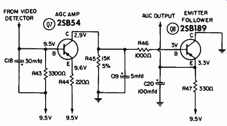
Fig. 10- 23. AGC amplifier configuration.
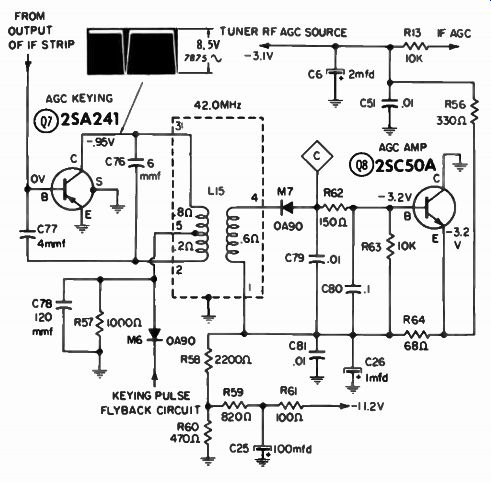
Fig. 10-24. Typical keyed-AGC system.
A typical keyed-AGC system is shown in Fig. 10-24. Q7 is an AGC amplifier that operates at the IF frequency. Note that Q7 is keyed by a pulse from the flyback section so that conduction occurs only during the horizontal-sync-pulse interval. Diode QA90 is a keying diode which ensures that only negative pulses are applied to the collector of Q7. The output waveform is a train of pulsed bursts, as shown in Fig. 10-20. This burst sequence is rectified by diode M7, which develops a negative de voltage across C79. Filtering is provided by C79, R62, and C80. In turn, the base of Q8 is negatively biased in accordance with the prevailing IF-signal level.
Transistor Q8 operates as an emitter follower in Fig. 10-24, in order to match the comparatively high impedance of M7 to the relatively low-impedance AGC line. Note that Q7 also operates as a de amplifier. When a fairly strong IF signal is applied to the base of Q7, the collector voltage changes very little because the keying pulse drives the transistor into saturation. However, de amplification is obtained because the IF signal increases the emitter current. The control range of an amplified AGC system is typically 25 db at each AGC-controlled IF stage.
Combination AGC and sync arrangements are used in some receivers. The first stage operates as an emitter follower, as shown in Fig. 10-25. Transistor Q33 operates with signal developed bias and rejects most of the video signal. Q34 is dc coupled to the emitter of Q33 and is reverse-biased. No polarity reversal occurs in this circuit from the base of Q33 to the base of Q34. Since Q34 operates at a comparatively low collector voltage, the sync signal is clipped both by reverse bias and by collector saturation. Q34 operates in a common-emitter configuration.
Separation of horizontal- and vertical-sync pulses takes place in the branch circuits connected to the collector of Q34. These branch circuits have differentiating and integrating circuits, respectively.
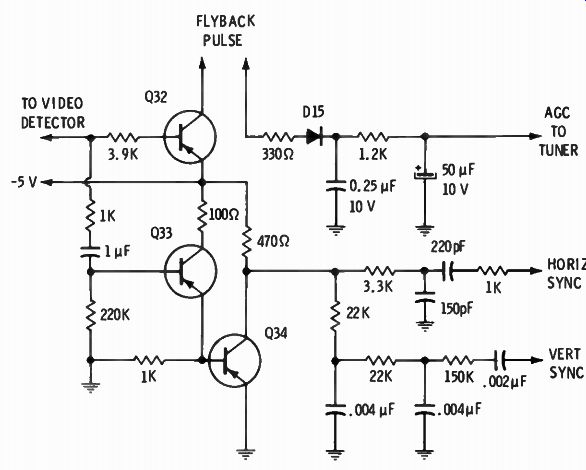
Fig. 10-25. Combination AGC and sync configuration.
Horizontal-sync pulses are processed in the network comprising the 3.3-ohm resistor, 220-pF capacitor, and 1-ohm resistor.
The horizontal sync pulses are fed into a resistive load (not shown in the diagram) so that the 220-pF capacitor forms a differentiating circuit. Note that this differentiator is preceded by an RC integrator comprising the 3.3-ohm resistor and 150-pF capacitor.
This integrator has a time constant of approximately 0.5 µsec and helps to minimize noise voltages by reducing the circuit band width as much as is practical. The highest frequency of importance in a horizontal-sync pulse is about 150 kHz. Noise pulses are comparatively narrow compared with sync pulses in most cases. In turn, bandwidth restriction assists in reduction of noise pulse disturbances.
Vertical-sync pulses are processed by the network comprising the 22-ohm resistor, 0.004-µF capacitor, second 22-ohm resistor, second 0.004-µF capacitor, 150-ohm resistor, and 0.002-µF capacitor in the collector circuit of Q34. This is a two-section integrator that builds up the vertical-sync pulse and opposes passage of horizontal-sync pulses. The 150-ohm resistor isolates the 0.002-µF capacitor and its subsequent resistive load from the integrator.
This capacitor and its load form an integrating circuit that assists in minimizing low-frequency transients in the vertical-sync output circuit. AGC voltage to the tuner is delayed by diode D15.
This AGC voltage is derived from a keyed-AGC stage (not shown in the diagram). Figure 10-26 shows basic AGC trouble shooting procedure.
SUMMARY
As indicated in Section 1, the combination of video, blanking, and sync signals is called the composite video signal. In addition to the video signal, which contains the actual picture, four additional signals must be transmitted before the picture can be properly displayed on the screen The horizontal-sync pulse is transmitted to keep the horizontal deflection circuit in step with the picture; the horizontal-blanking pulse is transmitted to blank out retrace; and the vertical-sync and vertical-blanking pulses are also transmitted to keep the vertical-deflection circuits in step and to blank the beam when it is returning from bottom to top.
The pulses occur when the electron beam in the picture tube is cut off. The pulses can be clipped from the signal at three different places in the circuit-at the video detector input, the video amplifying stages, or the point of restoration of the average background light of the picture.
Some television receivers employ more than a one-stage circuit to separate the sync pulses from the video signal. Additional stages are used to invert the phase of the pulses, clip the pulse width, amplify the pulse, level the pulse, and eliminate noise pulses to minimize interruption of sync and tearing of the picture.
Automatic gain control is used to minimize the effect of changes in signal strength at the receiver. The gains of the RF and IF stages are so regulated that a strong signal is amplified less than a weak signal. As a result, the TV picture tends to be relatively constant.
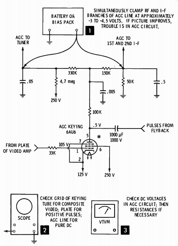
Fig. 10-26. Basic keyed-AGC troubleshooting procedure.
QUIZ
1. Why is a transistor amplifier with base input and collector output called a phase inverter?
2. Explain the basic clipper circuit.
3. Why are transistors more efficient than diodes in clipper circuits?
4. Why is interlaced scanning used?
5. What is the definition of AGC?
6. What is delayed AGC?
7. What is keyed AGC?