Television receivers have generally employed three types of circuit arrangements (or combinations of these circuits) to produce sawtooth waveforms for scanning purposes:
1. The multivibrator circuit, which has many variations, the most popular of which is shown in Fig. 11-1.
2. The blocking oscillator circuit, which permits the formation of a short pulse of energy. This pulse can be used to produce the sawtooth wave across a capacitor directly associated with the oscillator device, or the pulse can trigger a discharge device that acts as a switch across the capacitor. (See Fig. 11-2)
3. The sine-wave oscillator circuit, in which an oscillator of the correct frequency supplies the timing voltage for the discharging device. The sine-wave output of this oscillator is modified into short pulses by wave-shaping circuits. These pulses then operate a discharge device to produce sawtooth waves.
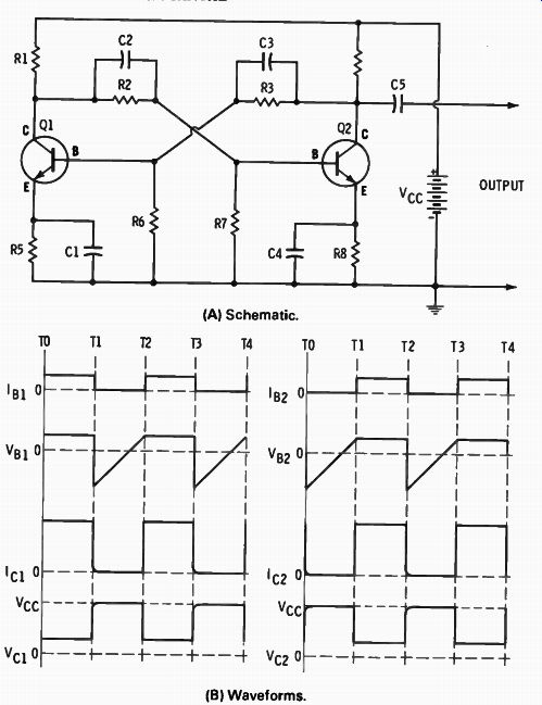
Fig. 11-1. Transistor multivibrator arrangement.
(A) Schematic. (B) Waveforms.
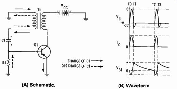
Fig. 11-2. Transistor blocking-oscillator arrangement.
(A) Schematic (B) Waveform
SAWTOOTH GENERATION
A sawtooth waveform is the basic deflection waveform, which can be generated in a suitable modified-blocking-oscillator con figuration, as shown in Fig. 11-3. Circuit action occurs as follows:
As transistor Q conducts, capacitor Cs charges toward the bias voltage level. As collector current flows, a transient voltage is induced into the base circuit by transformer T. The base is driven more negative, and the transistor is driven rapidly into saturation.
At this instant, Cs is fully charged, and flow of collector current stops. No more voltage is induced in the base circuit. Thus, the emitter is more negative than the base due to the charge on Cs, which cuts the transistor off. The transistor remains cut off while Cs discharges through Rs, producing the rising slope of a saw tooth wave. When Cs discharges sufficiently so that the transistor comes out of cutoff, positive-feedback action starts up once more, thereby forming the flyback portion of the sawtooth wave.
Observe that the vertical-sync pulse is coupled into the base circuit of Q in Fig. 11-3. Since R2 is normally adjusted so that the blocking oscillator has a slightly lower frequency than the sync pulse-repetition rate, the sync pulse triggers the transistor out of cutoff sooner than would occur in the free-running mode of operation; thereby, the sawtooth oscillator is synchronized. Resistor R2 establishes the oscillator frequency because it determines the bias level and, in turn, selects the time at which Q will come out of cutoff in the free-running mode. Diode X is a protective device connected across the primary of T to dissipate the inductive kickback surge that would otherwise cause transistor break down. The waveform V111 is described as a positive-going saw tooth because it rises from a more negative value to a less negative value.
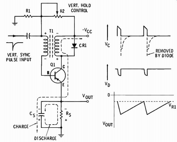
Fig. 11-3. Sawtooth-generating circuit of the blocking-oscillator type.
Some designs require a negative-going sawtooth waveform.
With reference to Fig. 11-4, Cs is uncharged at the time that the receiver is turned on. The base voltage on transistor Q is zero, and the transistor is cut off because of negative bias from R3; in turn, Cs charges through Rs to generate the falling slope of the sawtooth waveform. Meanwhile, the base bias on Q is becoming more negative because of R5.
There is a point at which Q suddenly goes into conduction.
Consequently, positive-feedback action via transformer T drives the base voltage highly negative, and the transistor goes into saturation. At this time, Cs rapidly discharges via T and Rs to ground, forming the flyback portion of the sawtooth wave. A sync pulse is fed to the base of the transistor to synchronize the oscillating frequency, as explained previously. A damping resistor R6 is connected across the primary of T to reduce the inductive kickback surge, thereby preventing damage to Q.
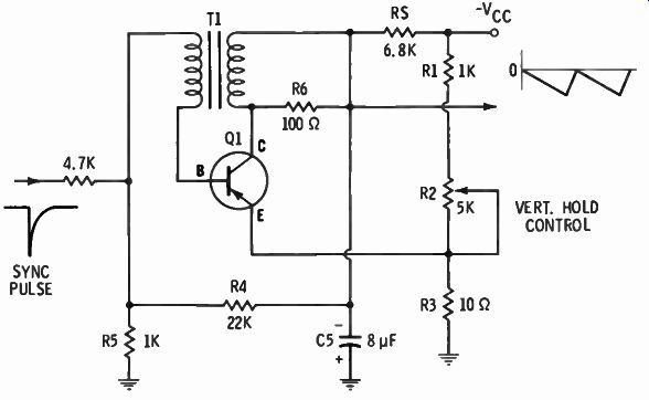
Fig. 11-4. Sawtooth-waveform generator that provides a negative-going output.
Next, consider the two-transistor, peaked-sawtooth multivibrator shown in Fig. 11-5. This is an example of the trend that has been taking place in the discard of separate oscillator and output stages and adoption of combined transformerless circuitry in which positive feedback takes place from the output stage. This circuit uses a common-emitter arrangement for both the input and output transistors. A diode is used as an electronic switch to charge and discharge the sweep capacitor in the feedback loop from the output transistor. Note that the instant power is turned on to the circuit, the voltage across the sweep capacitor Cs is zero. The diode is connected between Cs and a positive-bias voltage that is tapped off at the junction of R1 and R2. Initially, the diode is reverse-biased, and it isolates the sweep capacitor from RI and R2 as well as from the feedback circuit via Cs.
While the diode is reverse-biased, Cs charges through Rs to the value of the applied positive voltage. This rising positive voltage is applied to Q1 and forms the slope portion of the sawtooth wave. In turn, this rising positive voltage is applied across the deflection yoke. At the instant that the charge on Cs equals the voltage across R2, the diode starts to conduct and the voltage across Cs cannot increase further. Also, the sweep capacitor is connected to the feedback loop, and the voltage across the yoke falls quickly to zero. In other words, a regenerative discharge cycle starts, in which Cs discharges through the diode Cs and the yoke. A high amplitude negative kickback pulse is applied to the collector of Q2 at this time, causing Cs to discharge rapidly. Then the yoke voltage starts to swing positive, the diode cuts off, the feedback loop is disconnected, and Cs starts to charge once more.
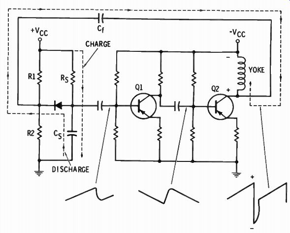
Fig. 11-5. Multivibrator peaked sawtooth-waveform-generator configuration.
A vertical-output circuit is always designed to provide a retrace blanking pulse for the picture tube. A blanking pulse of suitable amplitude and polarity is often obtained from a secondary winding, which is wound on the coupling choke, as depicted in Fig. 11-6. Thus, the coupling choke has a transformer construction, and it is sometimes called a vertical output trans former, although it is technically a blanking transformer and coupling choke. An RC wave-shaping circuit is used between the transformer and picture tube to change the peaked-sawtooth waveform into a pulse train.
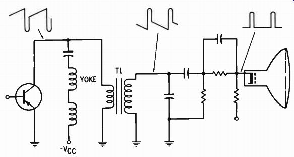
Fig. 11-6. Typical vertical-retrace blanking circuit.
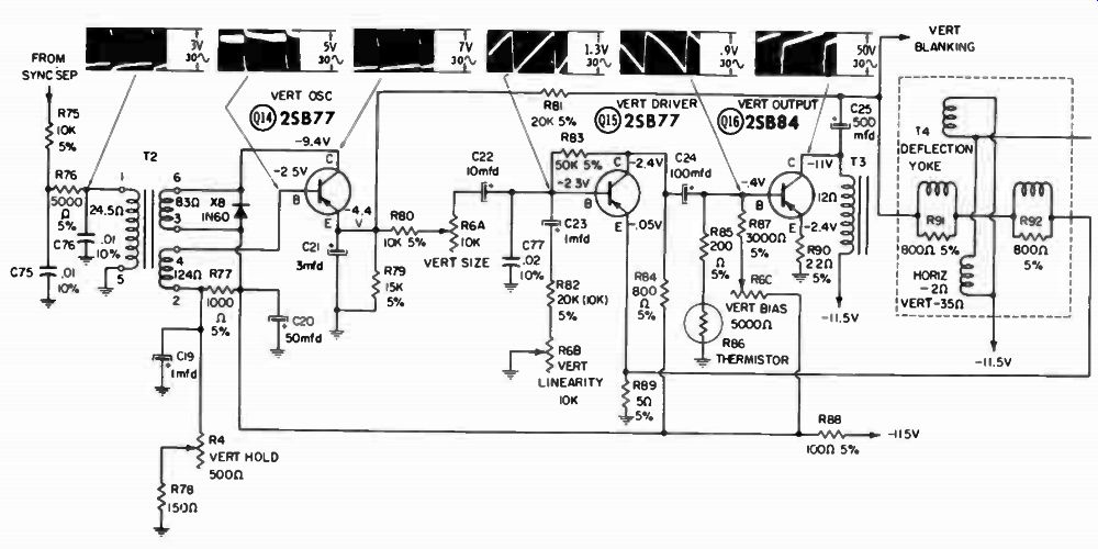
Fig. 11-7. Typical transistor vertical-sweep system.
In transistor TV receivers, blocking oscillators are commonly employed in both the vertical- and horizontal-deflection sections.
Figure 11-7 shows a typical vertical-oscillator configuration. The tightly coupled windings of transformer T2 provide positive feedback from collector to base of transistor Q14. This transistor operates in class C and conducts only for brief intervals; that is, the circuit operates as a pulse oscillator. During conduction, the base of Q14 is driven strongly by the amplified output from the collector. The base-emitter junction rectifies these negative going pulses and charges C21 negatively; after the passage of each pulse, Q14 is cut off, or blocked. Note that Q14 is reverse biased due to this blocking action.
With the emitter more negative than the base, Q14 (Fig. 11-7) remains cut off until C21 discharges sufficiently through R79 that the base voltage reaches the conduction level. Then, as Q14 comes out of cutoff, another sudden surge of oscillation occurs, after which Q14 is again blocked. The time at which the transistor comes out of cutoff is adjusted by varying the base bias with control R4. Vertical-hold control R4 is set to a point at which the blocking rate is somewhat slower than 60 Hz. Negative-going, vertical-sync pulses are coupled to the base of Q14 via T2. In turn, the sync pulses trigger the blocking oscillator into conduction a bit earlier than the stage would otherwise come out of cutoff, thereby obtaining vertical-sync lock.
Diode X8 in Fig. 11-7 prevents the transformer from applying an excessive peak voltage to the collector of Q14, which could result in damage to the transistor. The action of the diode can be explained clearly by considering a simpler blocking oscillator circuit that does not require a protective diode. Thus, in Fig. 11-8, the circuit action is as follows:
1. When a negative trigger pulse is applied to the base, the transistor begins to conduct. Collector current then flows through the transformer windings 3 and 4 and produces a varying magnetic flux, which induces a voltage of opposite polarity in windings 1 and 2. This voltage is coupled through capacitor CF to the base, thereby providing regenerative feedback. The transistor is quickly driven into collector saturation, and the collector current cannot rise further.
2. Since the collector current is now constant, T1 can induce no more feedback voltage into the base circuit; the base is now reverse-biased, and the transistor is cut off.
3. Stopping the collector current results in a collapsing magnetic field through windings 1 and 2, which induces a voltage in windings 3 and 4 that exceeds the supply voltage; this is seen as the backswing following the pulse in Fig. 11-8.
In this example, the backswing approximately doubles the collector voltage. Unless the transistor is rated for this peak value of collector voltage, the collector junction will break down.
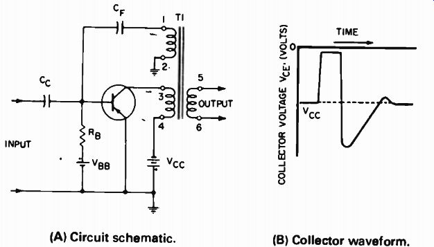
Fig. 11-8. Triggered blocking oscillator showing collector-to-emitter-voltage waveform.
(A) Circuit schematic. (B) Collector waveform.
With these points in mind, let us consider the action of diode X8 in Fig. 11-7 and observe how the backswing is eliminated. The current action is as follows:
1. When a negative trigger pulse is applied, transistor Q14 is driven from cutoff into conduction. The collector current suddenly increases due to feedback, and the collector voltage drops because of the voltage drop across windings 3 and 6.
2. As the collector voltage suddenly falls, diode X8 is reverse biased; therefore, X8 is effectively out of the circuit at this time. The transistor is quickly driven into collector saturation, and the collector current cannot rise further.
3. Since the collector current is now constant, T2 can induce no more feedback voltage into the base circuit. The base is now reverse-biased, and the transistor is cut off.
4. Stopping of the collector current results in a collapsing magnetic field through the windings, which quickly increases the collector voltage. However, the collector voltage cannot rise above the supply voltage because X8 then becomes forward-biased and short-circuits windings 3 and 6, thereby eliminating the backswing.
Next, let us consider a blocking oscillator utilized in a horizontal-oscillator section. With reference to Fig. 11-9, transistor Q20 operates as a blocking oscillator, and the time at which it comes out of cutoff (and hence its repetition rate) depends on the value of base-bias voltage. L16 and C99 form a ringing circuit that stabilizes the cutoff point for Q20 by superimposing a sine wave on the blocking-oscillator waveform.
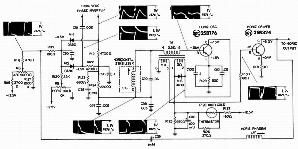
Fig. 11-9.
The action of the horizontal stabilizer is seen in Fig. 11-10.
When a ringing coil is not used, the decay of the voltage is exponential and approaches the cutoff level slowly. In turn, the instant at which conduction is initiated can vary appreciably due to slight voltage fluctuations or small noise voltages. On the other hand, when a ringing coil is used, a sine wave is superimposed on the exponential waveform, and the combined waveform approaches the cutoff level rapidly. Because of the steep slope of the waveform through the conduction level, the instant at which conduction is initiated does not vary to a disturbing extent even when small-noise voltages or other fluctuations are present.
Horizontal-stabilizer coil L16 is adjustable so that the optimum phase of ringing waveform can be utilized.
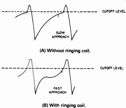
Fig. 11-10. Oscillator waveforms with and without a ringing coil.
(A) Without ringing coil.
(B) With ringing coil.
Regenerative feedback occurs from collector to base of Q20 in Fig. 11-9. This feedback is provided by the tightly coupled windings of transformer T5. As a result, blocking oscillation occurs.
Diode M16 short-circuits the backswing of the generated wave form, as explained previously. This prevents excessive peak collector voltage from being applied to Q20. Collector-current stabilization is provided by thermistor R128. If the temperature rises, the resistance of R128 increases, thus reducing the collector voltage and preventing Q20 from drawing increased current from the de supply.
Sine-Wave Generators
The familiar sine-wave oscillator can produce pulses that will trigger a discharge tube associated with a sawtooth-wave-forming capacitor. Only a short portion of the sine wave is used; it is passed through clipping stages to "bite off" a small section of the wave. The output of the clipper is a pulse. The usefulness of this type of circuit will be discussed in the section "Control of Scanning Generators by Sync Pulses"
SAWTOOTH-GENERATOR CONTROL AND PRODUCTION OF SCANNING WAVEFORMS
At this time, let us examine in greater detail the sawtooth scanning waves that produce the raster. We have mentioned before that the horizontal and vertical sawtooth motion of the electron beam must keep in step with similar sawtooth scanning movements occurring at practically the same instant in the camera tube at the transmitter.
To accomplish this synchronization, pulses that control the horizontal and vertical scanning are transmitted in the television signal. These pulses occur between each horizontal frame. During the scanning of the frame, the receiver is "on its own." however, during the short interval between successive horizontal frames, the deflection circuits of the receiver are the absolute "slave" of the transmitter if the set is well designed, operating properly, and being used in an area of adequate field strength.
How the synchronized pulses are separated from the complex signal has already been covered. At this point, we shall examine the relationship between the timing of these pulses and the control of the sawtooth scanning of the receiver. Figure 11-11 shows the sequence of events during the scanning of one horizontal line and during the return of the electron beam to start the scanning of the next line. The sawtooth line in Fig. 11-11 shows the desired linear trace and retrace motions of the electron beam in the TV picture tube. It does not necessarily depict the exact wave of current that must be passed through the deflection coils of the picture tube. As a matter of fact, we shall find later that the deflection current must be distorted somewhat to accomplish the linear sweep and rapid flyback of the beam of electrons tracing the picture.
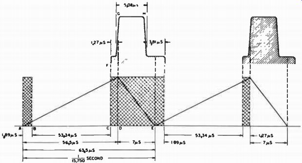
Fig. 11-11. Horizontal-scanning wave and synchronizing signal.
Figure 11-11 shows, therefore, the ideal sawtooth for control ling the horizontal scanning motion in a television receiver. At point A, the electron beam starts to cross the face of the picture tube horizontally from left to right. (We shall assume the picture tube is a 17-in, type and has an active picture width of 14 in.) The beam has blanked out from A to B, and the picture starts at point B. Between points B and C, as the uniform motion progresses, the video modulation produces the picture.
As stated previously, the picture frame consists of 525 horizontal lines reproduced each 1/3 0 sec (30 frames/sec x 525 lines per frame = 15,750 horizontal lines/sec). This means that the time for the trace of a line and its return to start another line is 1/15,750 sec.
We should introduce the idea of talking about these extremely short time intervals in multiples of one-millionth of a second. The unit of measurement is a microsecond (µsec), which is the length of time required for the completion of one cycle of carrier wave at the middle of the broadcast band, or 1,000 kHz. The entire horizontal action, including the tracing of the picture line and the return to start a new line, occurs in 63.5 µsec.
Let us divide the picture width (14 in.) by the time of active scanning (53.34 µsec). We obtain a velocity of 4.1 mi/sec. The retrace time (between retrace points D and E in Fig. 11-11) is 7 µsec. Since this retrace is over the same 14 in. of horizontal motion, the speed of the spot (blanked out to produce no light) must obviously be much faster. Actually, this retrace can reach a speed of 31.5 mi/sec.
As stated previously, the sequence of events must occur exactly in step with a similar sequence occurring at the same instant in the camera tube of the transmitter. To accomplish this action, pulses are sent out from the transmitter between each horizontal trace. The shape of these pulses is shown above the sawtooth wave shown in Fig. 11-11. At the instant shown as F, enough voltage appears at the grid of the picture tube to blank out all light. The region from F to G is known in television slang as the "front porch." This region is slightly more than one-millionth of a second in duration. At point G, the carrier wave of the transmitter abruptly increases by approximately 25 percent of its average value. This sharp rise in the carrier triggers the scanning generators in the receiver. The scanning generators produce the required sawtooth motion of the electron beam. (Exactly how the pulse accomplishes this triggering will be described later.) The horizontal beam does not trace a line parallel with the top of the picture but has a slight downward slope. This vertical motion is controlled by a scanning sawtooth, which moves the scanning spot to the bottom of the image and then rapidly returns it to the top. The electron beam moves from the top to the bottom of the picture and back to the top in '/60 sec. It is easy to see that this vertical scanning is much slower than the horizontal-line tracing action and requires 16,666 µsec. Pulses are sent out between successive fields to lock in, or control as a slave, the vertical-scanning oscillator of the receiver. A cycle of the vertical-deflection sawtooth wave, together with an enlarged section of that part of the wave which occurs during blanking and retrace, are shown in Fig. 11-12.
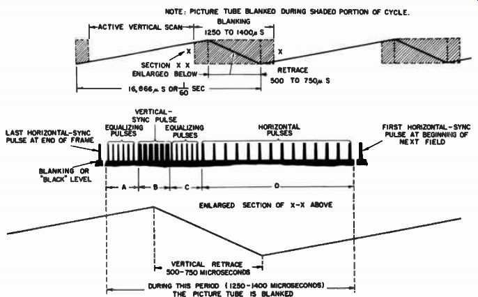
Fig. 11-12. Vertical-scanning wave and synchronizing signal.
The portion of the television signal that controls vertical retrace and synchronization is much more complicated than the single horizontal pulses, which occur between successive horizontal lines. The vertical-synchronizing signal resembles a comb with uneven teeth. If its only function were to trigger the vertical oscillator and blank out the picture-tube screen during retrace, it could be made in the form of a single, long, rectangular pulse whose time duration would be from 20 to 22 horizontal lines (1,250 to 1,400 µsec). However, the vertical-synchronizing signal must perform two other functions: It must continue to keep the horizontal-scanning oscillator in step during vertical retrace, and it must ensure that alternate fields have proper interlace of the horizontal lines.
Horizontal synchronization is kept in step by notches B and pulses A, C, and D (Fig. 11-12). Interlace is controlled by equalizing pulses A and C (Fig. 11-12) preceding and following the vertical-sync pulse.
CONTROL OF SCANNING GENERATORS BY SYNC PULSES
We have seen that the scanning systems of the receiver must keep in accurate step with the scanning raster of the camera tube at the transmitter, and that the synchronization pulses satisfy this requirement. For a satisfactory reproduced picture, the picture elements of adjacent horizontal traces must line up accurately, and the lines of alternate fields must interlace, or space, accurately between each other.
To avoid a displacement of more than one picture element in successive horizontal lines, the frequency stability of the horizontal oscillator must be 0.2 percent or better. Figure 11-13A shows horizontal displacement.

Fig. 11-13. Picture-element displacement that might result from scanning oscillator
instability. (A) Horizontal displacement. (B) Vertical displacement.
To avoid "pairing" of the lines of successive fields (the line lying on top of those of the preceding field instead of being properly interlaced), the stability of the vertical oscillator must be better than 0.05 percent. Figure 11-13 shows this displacement.
Note, in passing, that there are various receiver sections generally associated with the horizontal-output system. As shown in Fig. 11-14, these sections typically comprise the high-voltage system, ACC and AFC sections, horizontal oscillator, vertical sweep circuit, yoke, and picture tube. Thus, the horizontal-output system supplies feedback pulses to the ACC and AFC sections, boost voltage to the vertical-sweep circuit and horizontal oscillator, high voltage to the picture tube, and horizontal drive to the yoke. The horizontal oscillator supplies a drive signal, and the low-voltage power supply provides (B + (Vcc) voltage to the horizontal-output section. When checking the linearity of horizontal- and vertical-sweep action, an audio oscillator may be used, as shown in Fig. 11-15. Note that the extended high frequency output, up to 1.5 MHz, is required for checking horizontal linearity.
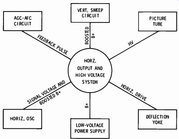
Fig. 11-14. Some circuits commonly associated with the horizontal-output and
high-voltage system.
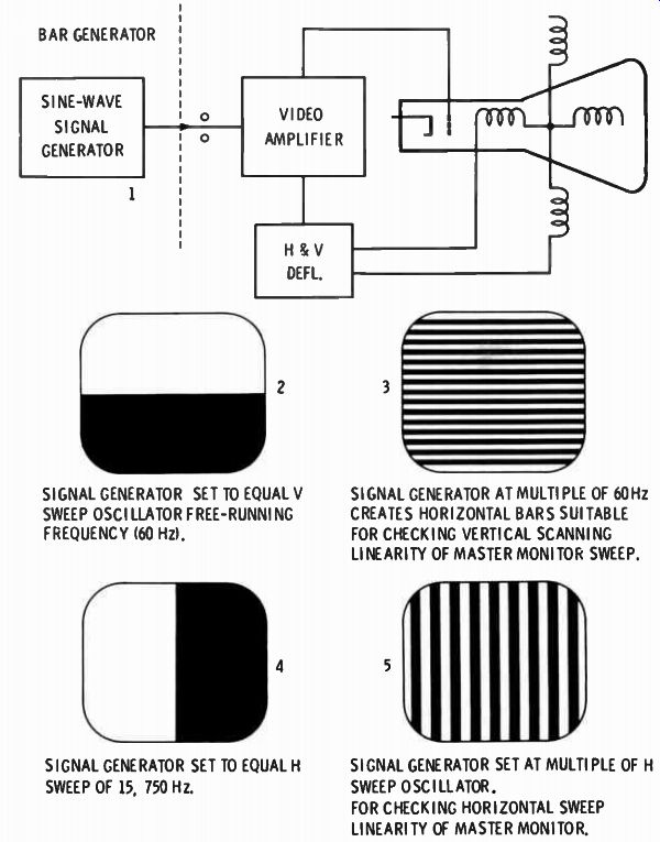
Fig. 11-15. Check of vertical- and horizontal-scanning linearity.
The horizontal and vertical pulses are clipped from the signal, amplified, and passed through circuits that classify the pulses so that each will control its own scanning oscillator only. The end result is a short, sharp "pip" for the horizontal control and a long, triangularly shaped pulse for the vertical control.
In considering how the pulse controls the oscillator frequency, three items are important:
1. Free-running frequency of the sweep generator-This frequency is that which would be generated at any particular setting of the hold control if the sync pulses were not pre sent. The frequency can be slower or faster than the pulse repetition rate or in exact step. Later we shall show that for proper stable operation, the slow rate is required.
2. Firing point of the sweep generator-This is the bias voltage required for the controlled device in order to initiate conduction in the discharge device and start capacitor discharge and scanning-wave retrace. At this point in the cycle the oscillator is most sensitive to control by the sync pulse.
3. Synchronizing frequency-This is the rate at which the pulses are applied to the control-input terminal of the oscillator: 60 hertz for vertical synchronization and 15, 750 hertz for horizontal synchronization.
Since the control action of the blocking oscillator can be diagrammed more readily, we shall consider it first.
Pulse Control of Vertical Blocking Oscillator
The triggering, or firing, of the blocking oscillator occurs when the bias voltage passes the cutoff point. The free-running frequency of the oscillator (if no sync pulses are present) is deter mined solely by the time constant of the base capacitance and resistance. Once the oscillator is fired, it functions on its own until it is blocked again by the base-cutoff voltage.
If a pulse of positive potential from an external source is fed to the base while the base capacitor is discharging through the resistor, the base voltage will pass the cutoff point and the device will begin to conduct. The sawtooth-forming capacitor will discharge, and retrace will occur; a new scanning cycle then begins.
Therefore, the repetition of the positive-sync pulses can control the firing of the blocking oscillator and lock the picture into synchronization.
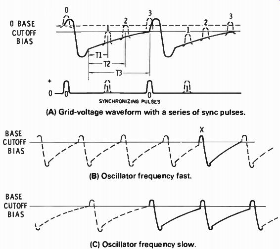
Fig. 11-16. Pulse control of a free-running oscillator.
(A) Grid-voltage waveform with a series of sync pulses. (B) Oscillator frequency fast (C) Oscillator frequency slow
Figure 11-16 shows this action in detail. Figure 11-16A is an enlarged portion of the blocking-oscillator base voltage. The synchronizing pulses below the base waveform show a series of pulses marked 0, with leading edges that are exactly in step with the wave. These pulses do not affect the free-running frequency of the oscillator. They merely add to the base voltage at the same instant it is being driven positive by the collector-current pulse.
On the other hand, if the sync pulses occur at the points indicated as 1, the pulse voltage added to the discharge voltage is still short of the cutoff bias point and will not fire the device. However, if the pulse occurs at points 2 or 3, the critical bias will be exceeded, the device will immediately conduct, and retrace will begin.
Since the free-running frequency of the blocking oscillator can be changed by varying the time constant of the capacitance and resistance in the base circuit, we shall examine this action under the following conditions: (1) oscillator running faster than the sync-pulse rate; and (2) oscillator running slower than the sync pulse rate.
Figure 11-16 shows what happens when the oscillator is running faster than the sync-pulse rate. The dotted portion of the waveform indicates lack of synchronization at that point. Notice that several cycles occur before the pulse reaches point X. At this point the base-cutoff voltage is exceeded and the tube fires.
Normally, you would expect the picture to lock in satisfactorily; however, this is not true. Lock-in occurs only momentarily during the field initiated at point X. Succeeding fields do not lock in.
With the oscillator running in this fast condition, the sync pulses occur during the scanning interval; consequently, the picture is divided by the blanking bar. Also, the oscillator, running faster than the sync-pulse rate, can easily be triggered into erratic operation by automobile ignition and static interference; therefore, the picture will be unstable. In modern receivers, however, improved circuit designs have resulted in more stable pictures even under heavy interference conditions.
Figure 11-16C shows what happens when the free-running frequency of the blocking oscillator is slower than the sync-pulse rate. Notice that lock-in occurs much faster and a good stable picture is obtained. This is obviously the desired condition because the oscillator should run slightly slower than the sync pulse rate. The sync pulses will then take over and force the blocking oscillator to lock in with each succeeding sync pulse.
The height and width of the sync pulses are not important as long as they are high enough to drive the base above the cutoff point.
With the sync-pulse amplitude reasonably high, the hold control can be varied over a fairly wide range without loss of synchronization.
For control of the blocking oscillator just described, the sync pulses are positive. Sync pulses can be made either positive or negative with respect to ground (or chassis), depending on receiver design.
Pulse Control of Transistor Horizontal Oscillator
The basic function of pulse control in a transistor-oscillator configuration is to provide horizontal-sync lock in a manner that rejects disturbing noise interference insofar as possible. This control of the horizontal-oscillator frequency is similar to that found in tube-type TV receivers. To minimize picture tearing or other disturbances due to random-noise pulses, the horizontal-sync pulses are processed in a comparator circuit that has a comparatively long time constant. The frequency of a horizontal oscillator, in turn, is controlled indirectly, and the noise-pulse voltages tend to average out and cancel.
Horizontal-sync pulses are mixed in a diode circuit along with comparison waveforms from the horizontal-sweep section. In turn, a de control voltage is developed that opposes any tendency of the horizontal oscillator to drift off frequency. The control voltage is applied through an RC network that has an appreciable time delay, so that successive noise pulses tend to cancel one another.
Figure 11-17 shows the plan of the pulse-control network. A basic AFC circuit is shown in Fig. 11-18. Sync pulses and the comparison sawtooth waves are fed into the diode circuit. In turn, the sync pulses ride on the sawtooth waves. Note that the peak-to-peak voltage of the combination waveform is thereby increased.
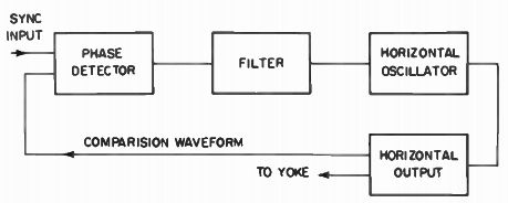
Fig. 11-17. Block diagram of horizontal AFC and deflection system.
Capacitor C in Fig. 11-18 can be charged only if one of the diodes conducts more than the other. If the oscillator happens to be exactly on frequency, both diodes conduct equally because voltages V1 and V2 are equal. On the other hand, if the oscillator tends to run too slowly, the waveforms are changed and D2 conducts more than D1. Hence, the upper terminal of C becomes negative, and a negative voltage is produced. If the oscillator tends to run too slowly, a positive control voltage is produced.
This control voltage is fed directly to the oscillator or to a control device; in either case, the control voltage corrects the oscillator frequency.
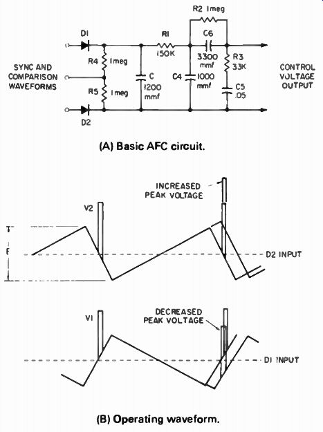
Fig. 11-18. Peak-voltage change when phase of comparison waveform changes.
VI (A) Basic AFC circuit. (B) Operating waveform.
The RC network to the right of C in Fig. 11-18 is basically an integrating and filter circuit that delays and smooths the control voltage. This configuration also provides a fast initial correction, followed by a slower correction in the same direction, which eases the oscillator to its correct frequency without overcorrection. When a defect occurs in this network, the result is often an overcorrection alternating with an under-correction, resulting in a symptom called the piecrust effect. Technicians term the circuit action as hunting when the picture has a piecrust or gear-tooth appearance (see Fig. 11-19).
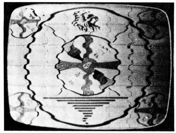
Fig. 11-19. Typical piecrust trouble symptom.
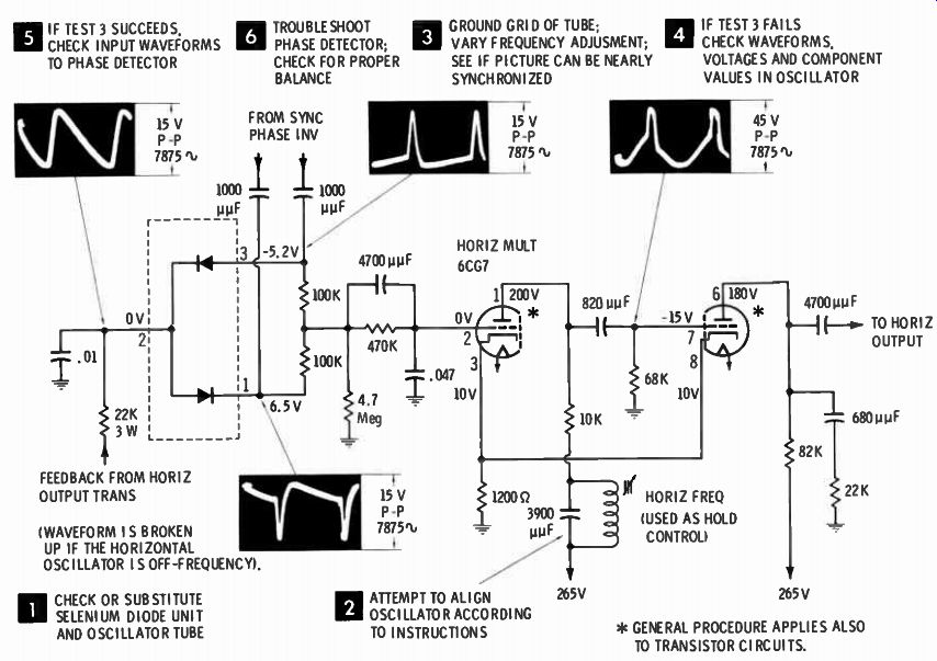
Fig. 11-20.
Summary of Scanning-Generator Pulse Control
1. A positive synchronizing pulse controls the frequency of a blocking oscillator.
2. A negative pulse controls the frequency of a cathode coupled multivibrator.
3. The free-running frequency of the scanning oscillator should always be slightly less than the synchronizing-pulse repetition rate; the hold, or frequency, control of the oscillator controls this action.
4. As the base voltage of a pulse generator approaches the "trigger" point, the oscillator becomes increasingly sensitive to control by additional base voltage. At this point, the scanning can be "tripped" by interference. Special circuit combinations have been devised that are controlled by the pattern of the pulses rather than by the individual pulses.
Such a system is relatively insensitive to interference, which seldom has a regular pattern. Figure 11-20 shows the basic troubleshooting procedure for a horizontal AFC and oscillator section.
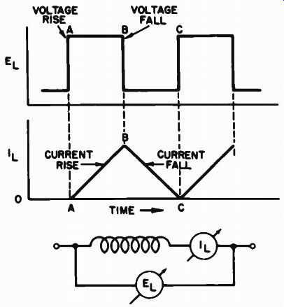
Fig. 11-21. Rise and fall of current through a pure inductance when a square
voltage wave is applied.
SCANNING
The amount an electron beam in an electromagnetically deflected cathode-ray tube is deflected depends upon the strength of the magnetic field produced by the deflecting coils.
The magnetic field is proportional to the amount of current passing through the coils, and these fields cross the path of the electron beam within the neck of the tube.
We must supply a linear sawtooth of current through the coil so that the electron beam will trace the proper raster under the combined influence of the horizontal- and vertical-deflecting coils. In Fig. 11-21 we see the resultant shape of a current wave that would flow through a pure inductance if a symmetrical square wave of voltage were applied across its terminals. This type of wave, as we have seen, can be developed by a conventional or symmetrical multivibrator. At point A, the voltage suddenly has been applied to the coil in much the same fashion as if a switch had been closed to connect the coil to a DC source of potential, for example, a battery.
Notice that the current through the coil did not immediately rise to maximum. The self-induced voltage of the coil opposed the sudden change. The current, therefore, increased linearly over that portion of the cycle when the applied voltage was steady. (Theoretically, the current rises exponentially; but for practical purposes, we can consider it to be a linear change.) At point B, the impressed voltage suddenly was removed (the switch was opened). At this point, the current did not immediately fall to zero since it was maintained by the energy stored in the magnetic field. The self-induced voltage of the coil served as the driving potential to produce the linear fall of current from point B to point C. We have now produced a triangular wave of current through the coil. If we can make the rise portion of the curve longer than the decay portion, we can produce the desired sawtooth scanning current wave by making the impressed voltage wave asymmetrical, as shown in Fig. 11-22.
Since a deflection coil cannot be built as a pure inductance, we must now consider what effect the resistance of the windings will have on the voltage waveform producing a sawtooth of current.
Figure 11-22 shows three types of circuits and the voltage wave form necessary to produce a sawtooth wave of current through each circuit. Figure 11-22A shows a pure resistance. The current is in phase with the voltage, and a sawtooth wave of voltage impressed across the resistor will cause a sawtooth wave of current through it. Energy losses occur only in the form of heat. The voltage required to produce a certain current is equal to the IR drop, as determined by Ohm's law.
Figure 11-22C shows the circuit represented by a deflection coil. The voltage waveform will be seen as a combination of the sawtooth of A and the rectangular wave of B (often called a trapezoidal waveform). In reality, this shape is the sum of an instantaneous pulse and a sawtooth. We might think of its function as follows:
1. The sawtooth, or linear rise, portion of the wave tends to produce a sawtooth wave of current through the resistive part of the circuit.
2. The instantaneous pulse portion of the wave forces a saw tooth wave of current through the inductive part of the circuit.
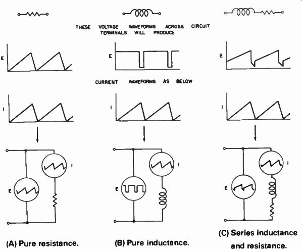
Fig. 11-22. Voltage and current waveform in inductive and resistive circuits.
(A) Pure resistance (B) Pure inductance (C) Series inductance and resistance.
To produce this combination waveshape, additional circuit elements are added to the sawtooth-capacitor-charging circuit.
The circuit is then known as a peaking type of waveshaping circuit. By proper choice of capacitor and resistor values, either the sawtooth portion or the impulse portion of the wave can be made to predominate. (The circuit action will be described later.)
It is interesting to note that one part of the wave must predominate over the other because of the difference between the horizontal- and vertical-deflection coils. In the vertical-deflecting coil, the resistive component predominates over the inductive component; thus, the sawtooth portion of the wave predominates over the impulse portion. For example, this coil might have a resistance of 68 ohms and an inductance of 50 mH. When the retrace rate is 60 hertz, a predominantly resistive circuit is presented.
In the horizontal-deflecting coil of the same receiver, the conditions are reversed; the inductive component predominates. The impulse portion is more important, and the required waveshape approaches that of Fig. 11-22B. For example, we would find a resistance of only 14 ohms and an inductance of 8 mH. Since this coil operates at the much higher frequency of 15,750 Hz/sec, the circuit is essentially inductive.
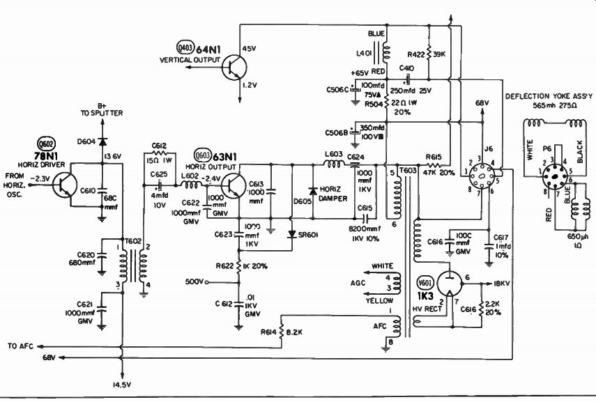
Fig. 11-23.
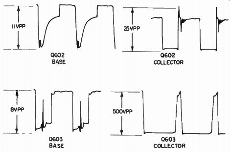
Fig. 11-24. Waveform found in horizontal-output system of Fig. 11-23.
TRANSISTOR HORIZONTAL-DEFLECTION SYSTEM
A typical transistor horizontal-deflection circuit is shown in Fig. 11-23. This is called a hybrid arrangement because a tube is used in the high-voltage section. The driver transistor Q602 is first cut off and then driven into collector saturation by the output from the horizontal oscillator. Figure 11-24 shows the normal waveforms at the base and collector of Q602. The rectangular waveform from the collector is transformer-coupled to the base of the horizontal-output transistor Q603. Q602 is said to operate in the switching mode, which means that the transistor is driven rapidly back and forth between cutoff and saturation.
Diode D604 in Fig. 11-23 helps to damp out the ringing of transformer T602 and also rectifies the overshoot to boost the +dc supply for the preceding phase-splitter stage. Q603 is operated in the switching mode. When Q603 conducts, the yoke current increases linearly. Meanwhile, capacitor C617 is charging. At the end of the forward-scan interval, the base waveform suddenly cuts off Q603. Due to the inductance and capacitance of the horizontal-output system, a ringing oscillation starts: Ringing begins with a large positive-overshoot pulse that quickly reverses the current through the horizontal-deflection coils and thereby initiates the flyback interval.
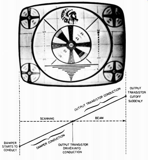
Fig. 11-25. Sequence of circuit action in horizontal-output system.
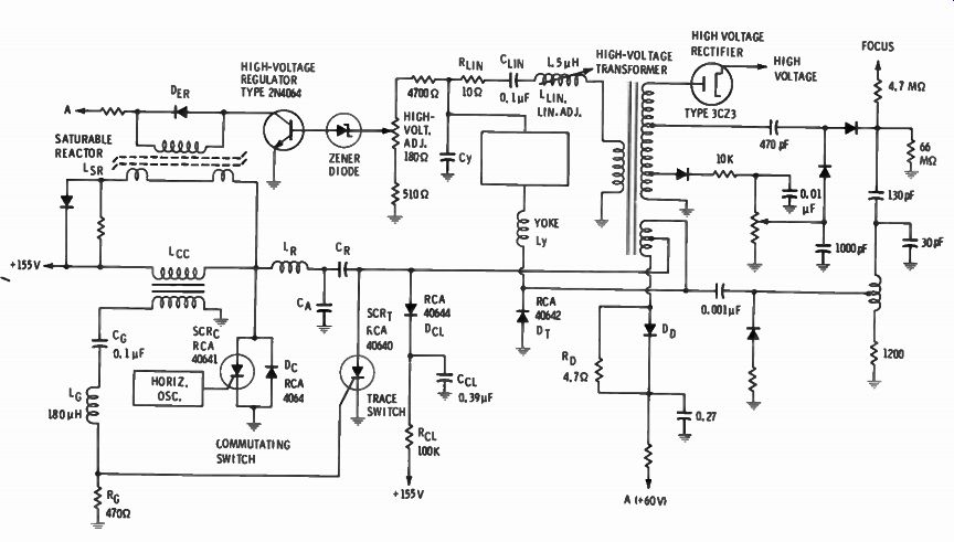
Fig. 11-26. Configuration of SCR horizontal-deflection system.
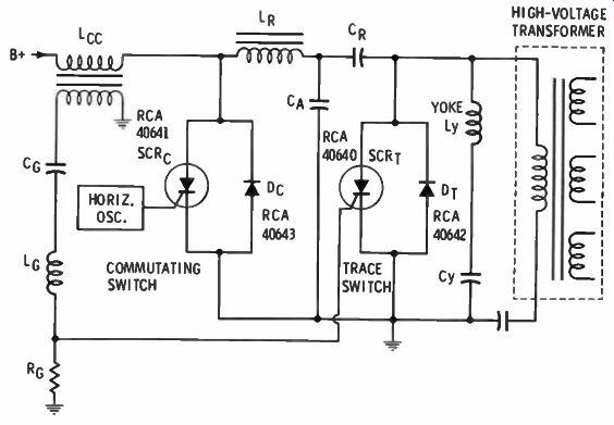
Fig. 11-27. Basic circuit that generates the deflection-current waveform.
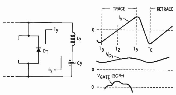
Fig. 11-28. Circuit action during first half of the trace interval.
As the negative half-cycle of ringing starts, damper diode D605 becomes forward-biased. In turn, the low impedance imposed by D605 limits the negative-ringing excursion. At the same time, C617 discharges linearly through the horizontal-deflection coils and D605 to ground. This linear discharge provides the first half of the ensuing forward-scan interval. Figure 11-25 shows this sequence of circuit action. To summarize briefly, the first half of the forward scan occurs while Q603 is cut off, and while C617 discharges through the yoke and D605. The second half of the scan occurs as Q603 is switched into conduction, and C617 proceeds to charge once more through the yoke.
Silicon controlled rectifiers (SCRs) are also used to a consider able extent in horizontal-deflection configurations. Figure 11-26 shows the arrangement of a typical system. It operates from an unregulated de power supply of +155 volts. Current and voltage waveforms required by the circuit action are obtained from LC resonant circuits. A regulator stage is included in the circuitry to stabilize scanning under conditions of varying line voltage and changes in picture-tube beam current. With reference to Fig. 11-27, the trace-switch diode DT and the trace-switch, silicon controlled rectifier SCRT provide the switching action that controls current flow in the horizontal-yoke windings Ly during the picture-tube, beam-trace interval. The commutating-switch diode Dc and the controlled rectifier SCRc initiate the retrace and control the yoke current during the retrace interval. .' Inductor LR and capacitors CR, CA, and Cy supply the required energy storage and timing cycles for the circuit action. Inductor Lcc provides a charge path for capacitor CR from the de supply voltage so that the system recharges from the receiver power supply. The secondary of inductor Lcc provides the gate-trigger voltage for the trace switch SCR. Capacitor CR determines the optimum retrace time by its resonant action with inductor LR. Figure 11-28 shows the voltage and current relations during the first half of the trace-deflection-current interval, from T0 to T2.
At time T0, the magnetic field has been established in the horizontal yoke windings L. This field generates a decaying yoke current i, that decreases to zero when the energy in the yoke winding is depleted at time T2. This current charges capacitor Cy to a positive voltage Vcy through the trade-switch diode DT. Note that, during the first half of the trace interval, just before T2, the trace-controlled rectifier SCRT is prepared to conduct by applications of a gate-voltage pulse VCATE. However, SRCT does not conduct until a forward bias is also applied between its anode and cathode. This forward bias is applied during the second half of the trace interval. Next, consider the second half of the trace interval. At time T2, current flow is no longer maintained by the yoke inductance, and Cy begins to discharge into this inductance.
The direction of current flow in the circuit is then reversed, and trace-switch diode DT becomes reverse-biased. Trace-switch controlled rectifier SCRT is then forward-biased by Vcy across the capacitor, and the capacitor then discharges into the yoke inductance through SCRT, as shown in Fig. 11-29. Capacitor Cy is sufficiently large that Vcy is almost constant during the complete trace and retrace cycle. This ensures a linear current rise through the yoke inductance Ly over the complete scan interval from TO to To.
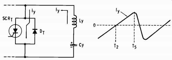
Fig. 11-29. Circuit action during second half of the trace interval.
Next, consider the start of the retrace interval. Figure 11-30 shows the components and the voltage and current waveforms that are involved. At time T3, before the end of the trace period, the commutating-switch-controlled rectifier SCRc is turned on by a pulse to its gate from the horizontal oscillator. CR is then permitted to discharge via SCRc and inductor LB. The current in this loop (the commutation circuit) builds up as a half-sine pulse.
At time T4, the magnitude of this current pulse exceeds the yoke-current value and the trace-switch diode DT again becomes forward-biased. The excess current in the commutating pulse is then bypassed around the yoke winding by the shunting action of diode DT. From T4 to T5, the trace-switch-controlled rectifier SCRT is reverse-biased by the amount of the voltage drop across DT. Therefore, the trace-switch-controlled rectifier is turned off during this interval, during which it recovers its ability to block the forward voltage that is subsequently applied.
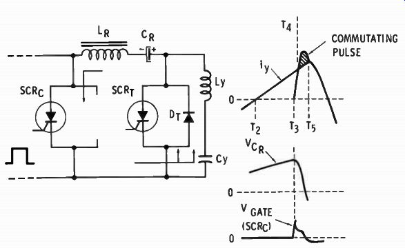
Fig. 11-30. Circuit action from time T3 to T5.
We shall next observe the circuit action during the first half of the retrace interval. At time T5, the commutating pulse no longer has a greater amplitude than the yoke current, as seen in Fig. 11-31. At this time, the trace-switch diode DT stops conduction.
The yoke inductance maintains the yoke-current flow. However, with SCRT in its off state, this current flows in the commutating loop comprising LR, CR, and SCRc. Note that time T5 is the start of retrace. While the current through the yoke windings decreases to zero, the energy supplied by this current charges capacitor CR to a voltage of opposite polarity as a result of resonant oscillation. At time T6, the yoke current is zero, and capacitor CR is charged to its maximum negative value. This circuit action completes the first half of the retrace interval.
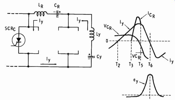
Fig. 11-31. Circuit action during the first half of retrace.
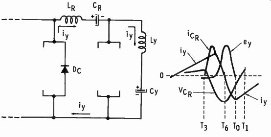
Fig. 11-32. Circuit action during the second half of retrace from T6 to T0.
Next, consider the circuit action that occurs during the second half of the retrace interval. At time Te, the magnetic energy in the yoke inductance is depleted and the stored charge in the retrace capacitor is then returned to the yoke inductance. This circuit action reverses the direction of current flow through the yoke.
During the reversal of yoke current, the commutating-switch diode Dc provides the return path for the loop current, as shown in Fig. 11-32. The commutating-switch-controlled rectifier SCRc is reverse-biased by the value of the voltage drop across diode Dc. Therefore, the commutating-switch-controlled rectifier turns off, and its voltage-blocking capability is recovered. As the yoke current builds up in the negative direction, the voltage across the retrace capacitor CR decreases.
Note that at the time To the voltage across capacitor CR no longer supplies a driving voltage for the yoke current to flow through the loop comprising LB, CR, and L. In other words, the yoke current finds an easier flow-path through the trace-switch diode DT, as shown in Fig. 11-33. This circuit action represents the beginning of the trace period for the yoke current or the beginning of a new cycle of operation at time To. Once that the negative-yoke current is decoupled from the commutating loop by the trace-switch diode, the current flow through the commutating circuit decays to zero. In turn, the stored energy in LR charges CR to an initial amplitude of positive voltage. Since the resonant frequency LB/CR is high, this energy transfer is accomplished in the short period from T0 to T1, as shown in Fig. 11-32.
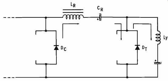
Fig. 11-33. Operation of deflection circuit during switchover from retrace
to trace at To.
We shall now follow the circuit actions in the recharging and resetting modes of system operation. The circuit actions required to restore energy to the commutating circuit and reset the trace SCR are also basic considerations in deflection-circuit operation.
Both of these actions involve inductor Lcc. During the retrace period, Lcc functions between the de supply voltage and ground via the commutating switch SCR or the diode (SCRc or Dc), as shown in Fig. 11-34. When the SCR and diode stop conducting, however, the path from Loe to ground is opened. In turn, the energy stored in Lec during the retrace interval proceeds to charge CR through the B+ supply, as shown in Fig. 11-35. This charging action continues through the trace period until the start of retrace. The resulting charge on CR resupplies energy to the yoke during the retrace interval.
Observe that the voltage developed across Lcc during the charging period of CR functions to forward-bias the gate electrode of the trace SCR, thereby readying this device for conduction. This voltage is inductively coupled from Lcc and is applied to the gate of SCRT via the wave-shooting network comprising CG, and RG. This signal voltage is applied to the gate of SCRT. The device conducts when a forward-bias voltage is applied from anode to cathode at approximately the midpoint of the trace interval. Next, it is helpful to observe the function of capacitor CA. It affects some of the circuit waveforms, as shown in Fig. 11-36, assists in turnoff of the trace SCR, and reduces the retrace time while providing increased energy storage in the circuit.
Fig. 11-34. Energy is supplied from L„ from T3 to T1
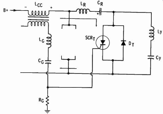
Fig. 11-35. Circuit action during the period from 1) to 13.
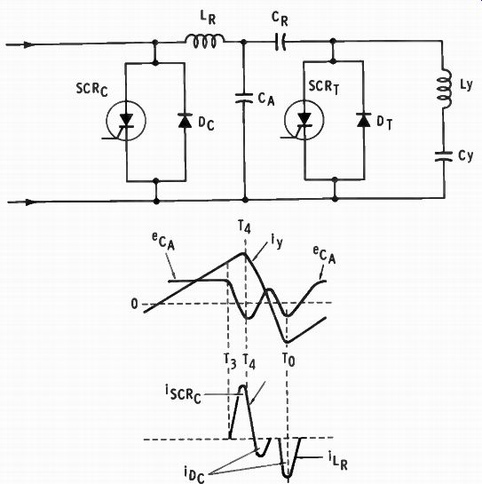
Fig. 11-36. Effect of CA with current and voltage waveforms.
During the larger portion of the trace interval, from T0 to T4 and including the interval from T3 to T4 while the commutating pulse is present, the trace switch is closed and CA operates in parallel with Co. From the start of the retrace at T4 to the beginning of the next trace interval at To, the trace switch is open. At this time, CA operates in series with Ly and Co so that the capacitance in the retrace circuit is decreased. In turn, the resonant frequency is decreased, thereby reducing the retrace time. Note that CA is also in parallel with LB. This operation changes the voltage- and current-deflection waveforms to some extent; in other words, the discharge around the loop occurs at a higher frequency than would otherwise take place. Troubleshooting of the deflection system is often facilitated by a careful checkout of the operating waveforms. Note that if an error is made and SCRc-Dc is interchanged with SCR T-DT, the deflection will operate almost (but not quite) normally.
TRANSISTOR VERTICAL-SWEEP SYSTEM
Operation of the blocking oscillator shown in Fig. 11-7 has been explained previously. The pulse waveform from Q14 is first changed into a sawtooth waveform by the same circuit that provides the time constant of the blocking oscillator, namely, C21 and R79. Discharge of C21 through R79 produces a curved (exponential) waveform, which is then linearized by means of negative feedback via R81. Manual control of vertical linearity is necessary, and this is provided by R6B, which operates in combi nation with C77 to introduce controlled waveshaping. The resulting sawtooth wave can be made either convex or concave by adjustment of R6B. Between these two extremes, the desired linear-sawtooth waveform is obtained.
It is also necessary to control the amplitude of base drive to Q15 in Fig. 11-7 in order to adjust the raster height; this is provided by control R7A. Negative feedback is also provided for Q15 and R89; that is, the waveform from the vertical-deflection coil returns to ground through the emitter resistor for Q15. Some additional negative feedback is also provided from collector to base of Q15 via R83. These negative-feedback circuits not only serve to produce basic linearity in the system, but also make tolerances on replacement transistors less critical than otherwise.
Any residual nonlinearity is corrected by adjustment of R6B. The vertical-output transistor shown in Fig. 11-7 employs a power transistor. Because of the comparatively critical bias that is required, a bias-control R6C is provided for maintenance adjustment. Q16 operates near its maximum-rated output, and since the collector current is heavy, the collector junction heats up appreciably. Although a heat sink (heavy metal mounting) is used, the transistor heats sufficiently in normal operation that the bias voltage must be stabilized. Unless the base-emitter voltage is stabilized, thermal runaway and resulting damage to the transistor will occur. R86 is a thermistor that operates to control the forward bias on Q16 and thereby stabilizes operation. When the emitter-base current tends to increase, R86 heats up and its resistance decreases, thereby decreasing the base voltage.
Since the vertical-deflection coils have both resistance and inductance, a peaked-sawtooth waveform is required to produce a sawtooth current through the coils. The negative peaking spike at the collector of Q16 is produced by inductive kickback from inductor T3 and the vertical-deflection coils. Note that although there are only 8.6 volts de between the collector and emitter of Q16, this inductive kickback generates a total peak-to-peak voltage of 50 volts for the output waveform. The peaking pulse is tapped off for vertical-retrace blanking of the picture tube. Negative feedback is provided by the unbypassed emitter resistor R90, which also assists in de stabilization of Q16.
SUMMARY
The multivibrator, blocking oscillator, and sine-wave oscillator are three types of circuit arrangements generally used to produce sawtooth waveforms for scanning purposes. One of the most popular circuits is the multivibrator because devices can act as automatic switches to control the charge and discharge of capacitors.
The horizontal and vertical pulses are clipped from the signal, amplified, and passed through circuits that classify the pulses so that each will control its own scanning oscillator only. The end result is a short, sharp pip for the horizontal control and a long, triangularly shaped pulse for the vertical control. The height and width of the sync pulses are not important as long as they are high enough to drive the grid above the cutoff point.
QUIZ
1. What three circuits are used for scanning purposes?
2. Which circuit for scanning is most popular?
3. How does an SCR deflection circuit operate?
4. Sync pulses can be either positive or negative. Which pulse is ideal for the cathode-coupled multivibrator?
5. What type oscillator is generally used in transistor television receivers?