Power supplies in television systems are more complicated than those normally found in radio and other electronic devices.
At least two separate and basically different load conditions must be provided for in the set:
1. A low-voltage, high-current system to power the oscillator, amplifier, and similar stages where applied potential does not exceed 450 volts. In addition, some receivers power the modulation and deflection systems from this source.
2. A high-voltage, low-current system to supply the accelerating anode potential for the cathode-ray or picture tube.
LOW-VOLTAGE, HIGH-CURRENT SUPPLIES
The signal-reception portion of the receiver, which includes sound and video amplifier or control tubes, presents a power requirement that does not differ greatly in voltage range from that of other electronic devices. Therefore, this portion of the television power supply is similar to the one found in large radio receivers.
In general, the voltage requirement is no more than 450 volts.
The current required, however, is frequently much greater than that necessary for radio operation. In addition, a good supply regulation is needed to operate the sawtooth oscillators for deflecting the electron beam of the cathode-ray tubes. These oscillators tend to produce currents in the power supply. If not properly filtered, these currents would appear as serious modulation hum in the beam control and sound circuits.
Early receivers required heavy-duty power supplies to provide the current (as much as 300 mA in some receivers) drawn by the 30 to 40 tubes in the receiver. These supplies employed from one to three rectifiers; the number, of course, depended upon the current requirements and the designer's preference as to voltage and current distribution.
Practically all power supplies use one of the basic rectifier circuits: the half-wave rectifier, the full-wave rectifier, or the bridge rectifier, as shown in Fig. 12-1. Half-wave- and bridge rectifier circuits may be modified to provide power supplies that have two different output voltages. These output voltages may have different values and the same polarity or the same values and different polarities. Polarity is defined with respect to ground. For example, Fig. 12-2 shows a basic half-wave rectifier arrangement that provides a positive-output voltage via diode A. In addition, a negative-output voltage may be obtained by connecting diode B in reversed polarity to the "hot" end of the secondary winding.
Dual-output voltages can also be obtained from bridge rectifiers. An advantage of a bridge rectifier is that it does not require a center-tapped transformer. However, in case the center-tapped transformer is utilized with a bridge-rectifier configuration, a power supply can be provided that has two output voltages.
Addition of a grounded center tap, as shown in Fig. 12-3, permits each half of the bridge rectifier to function as an ordinary two diode, full-wave rectifier of a chosen polarity. If one end of the bridge is grounded, as shown in Fig. 12-3B, the arrangement functions as an ordinary bridge rectifier that provides a high output voltage at the ++ terminal, and as a two-diode, full-wave rectifier that provides half as much output voltage at the + terminal.
The next step in complexity concerns voltage multipliers.
These are configurations that supply de voltages that are multiples of the ac input voltage.
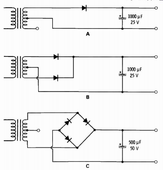
Fig. 12-1. Three basic rectifier circuits.
Full-Wave Voltage Doubler--The circuit shown in Fig. 12-4C can be modified by removing the ground connection between the two capacitors, and a standard full-wave, voltage-doubler arrangement is obtained, as shown in Fig. 12-4A. Note that two half-wave rectifier circuits of opposite polarity have been combined, with the output taken from across both capacitors to obtain double-output voltage. A voltage-multiplier circuit is often used in equipment where a high de output voltage is required from a transformerless power supply.
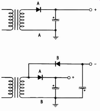
Fig. 12-2. Dual-output, half-wave rectifier arrangements.
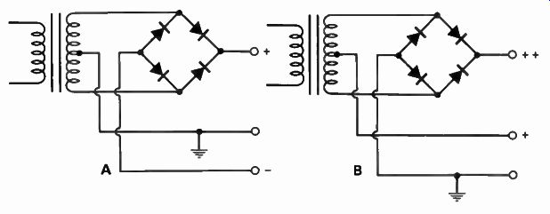
Fig. 12-3. Dual-output, bridge rectifier configurations.
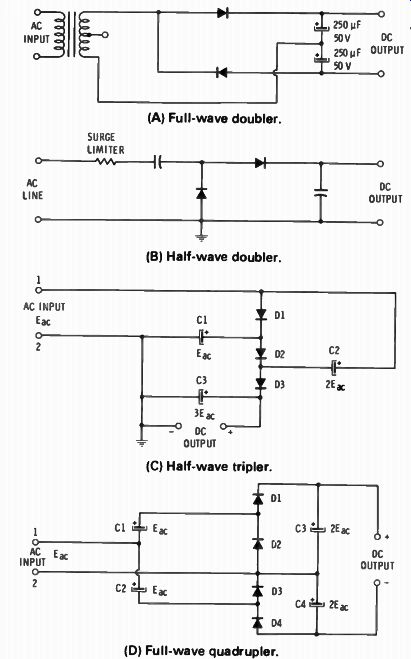
Fig. 12-4. Voltage-multiplier configurations. (A) Full-wave doubler.
(B) Half-wave doubler. (C) Half-wave tripler. (D) Full-wave quadrupler.
Half-Wave Voltage Doubler--A standard half-wave doubler arrangement, shown in Fig. 12-4B, is often preferred to the full wave arrangement. An advantage of the half-wave doubler is that it does not require a transformer. On the other hand, a half wave doubler has a ripple frequency equal to the line frequency, whereas a full-wave doubler has a ripple frequency equal to twice the line frequency. In turn, larger filter capacitors are required in the half-wave doubler arrangement.
Half-Wave Voltage Tripler--A half-wave voltage tripler operates on the same basic principle as a half-wave voltage doubler.
Fig. 12-4C shows the tripler configuration. Since it uses a ground connection to one input line, a transformer is not required.
Full-Wave, Voltage Quadrupler and Sextupler--When two half-wave voltage doublers are connected so that their outputs are effectively in series, a full-wave, voltage-quadrupler arrangement results, as shown in Fig. 12-4D. In the same manner, a full-wave voltage sextupler results from connecting two half wave voltage triplers so that their outputs are effectively in series.
Note that the comparatively complex quadrupler and sextupler arrangements are practical because their semiconductor rectifiers require no heater windings and heater circuits. In other words, their production cost is not excessive.
As a practical note, the foregoing voltage-multiplier circuits use capacitor input filters, and their voltage regulation (reduction of output voltage with increased current demand) is comparatively poor. Under heavy current demand, the output voltage may decrease as much as 30 percent, which can be minimized by the use of very-large-filter capacitors.
Filter Arrangements
Since a semiconductor rectifier has a very low voltage drop in its forward-conduction state, surge currents drawn by filter capacitors must be limited to avoid rectifier damage. With reference to Fig. 12-5, the starting surge is limited to some extent by the series impedance of the transformer winding.

Fig. 12- 5 Example of surge-current paths for two basic filter circuits.
However, if the series resistance of the transformer winding is low and capacitor C has a large value, a starting-current surge can result that damages the rectifier. Capacitor input filters are especially vulnerable to starting current surges. Therefore, it is poor practice to replace an input-filter capacitor with a higher value than specified in the receiver service data. In other words, when the power is turned on, a large current flows through the rectifiers to charge the input-filter capacitor. At the moment of starting operation, the input-filter capacitor appears as a dead short, and the momentary current demand can be extremely high. Therefore, it is often necessary to include circuit means to limit the initial charging current.
Choke-Input Filters--Power supplies that use choke-input filters do not require surge-limiting means. Note that the filter choke shown in Fig. 12-5B limits the surge current in the same manner that it limits the peak-rectifier current during maximum current demand.
Resistor Surge Limiter
With reference to Fig. 12-6, a small-valued resistor is often included in series with the ac input to the rectifier. Its value is chosen to limit the surge current to the maximum amount that the rectifier can handle for a short time. Note that surge-current ratings are generally much greater than the average de rating for a rectifier.

Fig. 12-6. Typical low-voltage supply using a surge resistor.
For example, a silicon rectifier that is rated for an average current of 750 mA has a surge-current rating of 35 A for 4 msec.
Observe, also, that the series resistance that limits the surge current is chosen with the worst case in mind. Thus, the worst case occurs when power is applied at the instant the ac voltage is swinging through its positive peak, and the input filter capacitor has zero charge. In the example of Fig. 12-6, the maximum input voltage is 127 volts rms; its peak voltage Is 180 volts, accordingly.
In turn, to limit the surge current to 35 A, the surge-limiting resistor should have a value of 5.2 ohms, in accordance with Ohm's law.
Following the initial current surge, the filter capacitors become fully charged. Thereafter, the voltage drop across the surge resistor is small. For example, if the current demand in Fig. 12-6 is 300 mA, the drop across the surge resistor will be 1.56 volts. In practice, transformer power supplies may or may not require a surge resistor with a capacitor-input filter, depending on the winding resistance of the transformer secondary.
DC VOLTAGE REGULATORS
A basic power supply has significant internal resistance. For example, rectifier diodes have a certain forward resistance, and transformers and chokes have winding resistance. In turn, there is an IR drop across the internal resistance of a power supply that is directly proportional to the current demand, and the output voltage is reduced by the amount of internal voltage drop.
Another factor that reduces the output voltage with increased current demand is the fact that the filter capacitors do not charge up to the same voltage as when the discharge rate is small. When the output voltage drops considerably under heavy current demand, the power supply is said to have poor regulation. Note that changes in ac input voltage also cause changes in de output voltage.
Zoner-Diode Regulator
Zener diodes are used in configurations such as shown in Fig.
12-7 to regulate the output voltage. The breakdown voltage of typical zener diodes ranges from 3.9 volts to several hundred volts. Two or more zener diodes may be connected in series to regulate voltages higher than the breakdown value of a single diode, as shown in Fig. 12-8. Various regulated voltages can be tapped off from a series arrangement of diodes, if needed. The value of the series dropping resistor must be sufficient that the maximum current rating of any diode is not exceeded under worst-case conditions. If the source voltage varies considerably, the cascaded regulator arrangement shown in Fig. 12-9 is more appropriate.
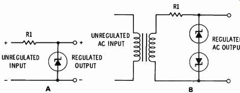
Fig. 12-7. Basic zener-diode-regulator arrangements.
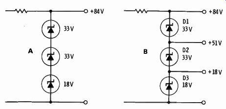
Fig. 12-8. Stacked zener-diode configuration.

Fig. 12-9. Cascaded zener-diode-regulator arrangement.
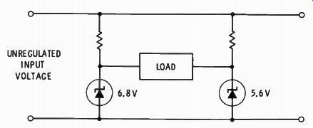
Fig. 12-10. Zener-diode configuration for regulation of small valves.
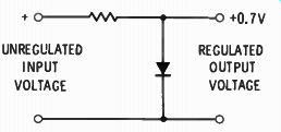
Fig. 12-11. Basic circuits for very-low-voltage regulation with a forward
biased diode.
Low-Voltage Zoner Regulators
Regulation of very low voltage is done on a differential basis, as shown in Fig. 12-10. The diodes are selected so that the difference in their breakdown voltage values is equal to the regulated voltage value that is required. The load is connected between the ungrounded terminals of the zener diodes. In the example of Fig. 12-10, the regulated voltage value is 1.2 volts. Note that zener diodes are never connected directly in parallel with each other.
Another method of obtaining low-voltage regulation is to use a forward-biased diode, as shown in Fig. 12-11. The forward voltage drop across a conducting semiconductor diode is relatively constant over a comparatively great current range. A forward biased diode can regulate voltages in the range from 0.5 to 1.1 volts, depending upon the type of diode that is used. Note that the efficiency of regulation is not as good as provided by zener arrangements.
Transistor Voltage-Regulator Arrangements
Low-voltage-regulated power supplies often use transistors.
This is accomplished by means of some form of feedback circuit that senses any change in the dc output voltage and, in turn, develops a control voltage that operates to cancel the change.
The control that is operative in the feedback or regulator circuit is a function of the circuit arrangement and may be a series or a shunt configuration.
In a transistor type of regulator, the output voltage developed by the dc power supply is compared with a reference voltage.
The difference between these voltages is amplified and fed back to the base of a pass transistor, either linearly or in the switching mode, thereby regulating the value of the output voltage. In case the pass transistor can be operated at any point on its characteristic between cutoff and saturation, the regulator circuit is said to be a linear voltage regulator. On the other hand, if the pass transistor operates only at cutoff or at saturation, the circuit is said to be a switching regulator.
SERIES-REGULATOR OPERATION
A series-regulator configuration uses a pass transistor that is connected in series with the load. In turn, regulating action takes place by a circuit that senses any variation of current flow through the series-pass transistor due to a change in line voltage or in current demand from the power supply.
A corresponding change in voltage drop across the pass transistor in consequence of feedback circuit action will be in opposition to changes in line voltage or to current demand, so that a practically constant voltage drop is maintained across the load.
By way of comparison, a shunt regulator uses a pass transistor connected in parallel with the load, and a voltage dropping resistor is connected in series with this parallel circuit branch. In turn, if the load-current demand changes, the current flow through the pass transistor will increase or decrease as required to maintain a virtually constant current flow through the dropping resistor.
As noted previously, the series-voltage regulator functions with a pass transistor connected in series with the load. Consequently, regulation takes place as the result of variation in the voltage drop across the series transistor. Note that the small-load efficiency of a series regulator can be much greater than that of a shunt regulator inasmuch as no output current is wasted through a branch path shunting the output. However, the full-load efficiency of the series and shunt regulators is about the same.
A basic series-voltage-regulator arrangement is shown in Fig. 12-12. Observe that a de amplifier is used to step up the error (difference) voltage obtained from a comparison between a sample of the output voltage and the reference voltage. This amplified error voltage is then applied to a regulating transistor connected in series with the load. The control voltage is developed across the regulating transistor and is applied to the error detector and amplifier. This error amplifier and the series transistors may include any appropriate number of transistor stages.
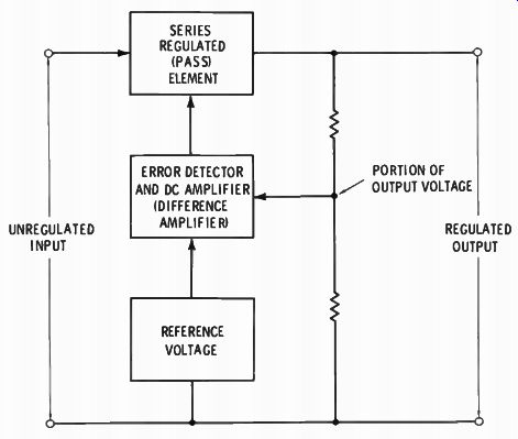
Fig. 12-12. Arrangement of basic series-voltage regulator.
Observe the simple series-regulator circuit depicted in Fig. 12 13. The transistor operates in the emitter-follower mode. Input voltage for the transistor is obtained from across the zener diode.
Note that the resistor provides breakdown current for the zener diode and also base current for the transistor. This configuration provides a considerable degree of regulation, which is ample for many applications.
Any change in the unregulated input voltage will cause a change in the breakdown voltage of the zener diode, thereby causing a small change in the regulated output voltage. Note that the load "sees" an output resistance, which is slightly higher than the emitter input resistance of the transistor. This output resistance has a value of approximately 30 ohms with a load-current demand of 30 mA, and it drops to about 1 ohm with a 1-A current demand.
Two general methods are used to apply voltage gain to a series-regulator transistor. One method, shown in Fig. 12-14A, operates the series transistor in the emitter-follower mode. This method places the input to the series transistor between its emitter and collector, with the output voltage taken between the collector and emitter. In the second method, shown in Fig. 12-14B, the transistor functions as a common-emitter amplifier. This method applies the control voltage between the base and emitter, with the output voltage taken between the collector and emitter.
Both of these methods have approximately the same performance. Note that the differential amplifiers shown in Fig. 12-14A and B function as difference or error amplifiers. They are basically high-gain, direct-coupled arrangements that provide low noise, low drift, and high stability when operated in a feedback loop. Because a differential-amplifier configuration is often used as a difference amplifier, the arrangement is commonly called a differential amplifier.
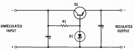
Fig. 12-13. Configuration of simple series-voltage regulator.
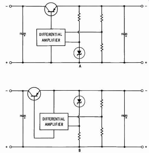
Fig. 12-14. Examples of series-regulating arrangements using error feed back
and amplification.
If a wide-output voltage range is required, the emitter-follower arrangement has an advantage because the voltage applied between the base and emitter is always low, regardless of the output voltage from the regulator. In most cases, it is convenient to have the output from the entire regulating amplifier approximately equal to the emitter voltage of the series transistor. Only a voltage-sensing lead is connected to the other output terminal.
Accordingly, there is no limitation placed on the regulator-output voltage by the regulating amplifier.
By way of comparison, an emitter-follower configuration operates the regulating amplifier at about the same voltage as the output lead, which does not include the series transistor. In turn, the regulating amplifier senses the voltage across the output terminals and drives the base of the series transistor. Note that the voltage of the base with respect to the regulating amplifier may be too high when used in a high-voltage regulator, and a dangerously high collector-emitter voltage may be required in the last transistor stage of the regulating amplifier.
The collector-emitter voltage will be comparatively constant in nonadjustable regulator arrangements. In turn, a large portion of the voltage may be divided by a zener diode connected in series with the collector. On the other hand, a wide-range voltage regulator cannot use this method of voltage division.
It is instructive to note that both arrangements shown in Fig. 12-14 are similar in various other respects also. Thus, the voltage divider senses the output voltage from the power supply and develops an input voltage that is applied to the differential regulating amplifier. In turn, the output voltage changes by feedback action to equal the voltage on the zener-diode reference source. As in ordinary power supplies, the electrolytic capacitors assist in ripple filtering and protect the regulator devices against high transient voltages. Observe that a regulated power supply has very considerable inherent filtering action, and that the ripple voltage is normally very small. However, some capacitive filter action is required between the rectifier(s) and the regulator. Also, the effective internal impedance of a regulated power supply is very low.
A series-regulating device may consist of a single very-high power transistor or several power transistors may be connected in parallel, as shown in Fig. 12-15. In such a case, the base-current (control-current) demand may be greater than can be supplied by the error amplifier. To meet this requirement, a Darlington pair may be employed, as shown in Fig. 12-15B. In this circuit, transistor Q2 operates in the emitter-follower mode and drives the series-regulating transistor Ql. Observe that, due to the current gain provided by Q2, the control current required from the error amplifier is reduced by a factor equal to the beta value of the emitter-follower transistor Q2. For example, if Q2 has a beta value of 50, and the series-regulating transistor Q1 requires a 10-mA control current, the error amplifier must provide only 0.2 mA of control current.
A series-regulator arrangement does not have inherent over load protection, and it can be destroyed by a momentary short circuit across the output terminals unless suitable protective measures are provided. For example, an overcurrent-sensing circuit may be included, which automatically limits the value of output current. Of course, voltage regulation is absent past the current limiting point.
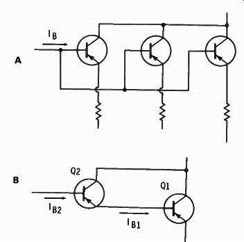
Fig. 12-15. High-power-regulating arrangements.
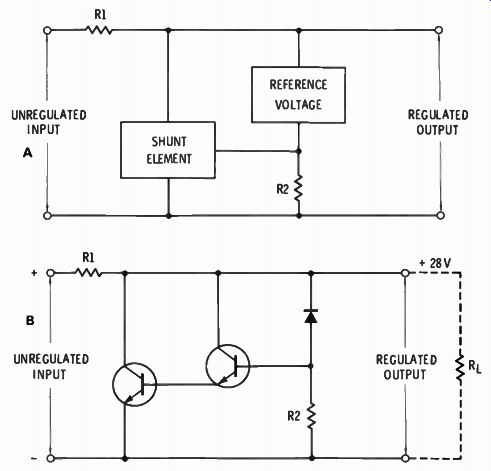
Fig. 12-16. Basic shunt-regulator arrangement.
SHUNT-REGULATOR ARRANGEMENTS
Although shunt regulators often have comparatively simple circuitry, they are usually least efficient for voltage regulation.
An advantage of a shunt-regulator configuration includes a shunt device and a reference-voltage element, as shown in Fig. 12-16A. Observe that the output voltage remains constant because the shunt-element current changes as the load current varies or as the input voltage changes. Any current change is reflected as a voltage change across R1, which is connected in series with the load.
Note that the shunt transistor connected in parallel with the load operates in the common-emitter configuration. For high power applications, several transistors may be connected in parallel or in a Darlington configuration. A Darlington pair is utilized in the example of Fig. 12-16B. An arrangement such as the one shown in Fig. 12-17 provides very close regulation of the output voltage.
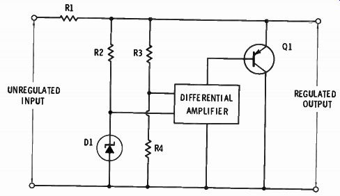
Fig. 12-17. Configuration that provides close regulation of the output voltage.

Fig. 12-18. High-voltage rectifier assembly using a stack of 13 semiconductor
diodes.
In some receivers, series-connected semiconductor diodes are used for high-voltage rectification, as shown in Fig. 12-18. Semi conductor diodes are also used instead of rectifier tubes in voltage-multiplier circuits. They provide simplicity and lower manufacturing cost because no filament supply is required. Figure 12-19 shows basic troubleshooting procedures.
SUMMARY
Power supplies in television receivers are generally more complicated than those normally used in radio and other electronic equipment. A low-voltage, high-current supply must be used to feed video IF, sound amplifier, and other similar stages where applied potential will not exceed 450 volts. In addition a high voltage, low-current system is needed to supply the accelerating anode potential for the picture tube.
The introduction of semiconductor rectifiers offered an opportunity to simplify and lighten receivers by eliminating the heavy and bulky power transformers. Some circuits have one disadvantage: The chassis is connected to one side of the power line, and so the user could receive a dangerous electrical shock between the chassis and any grounded metal object.
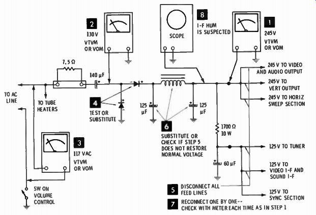
Fig. 12-19. Basic troubleshooting procedures for a semiconductor power supply.
The flyback system of obtaining high voltage is used in nearly all modern TV receivers. It uses a high-voltage pulse created in the output circuit of the horizontal amplifier during retrace. This high voltage is then fed to a rectifier, where it is rectified and filtered and becomes a high-anode potential for the picture tube.
QUIZ
1. What are the advantages in using semiconductors in the power supply?
2. What can be used in a power supply to eliminate electrical shock?
3. How many different types of high-voltage power supplies have been used in television receivers? Name them.
4. What are the voltage and current requirements for low voltage power supplies? High-voltage?
5. What is the approximate high-voltage potential in modern TV receivers?
6. What method is used in nearly all modern TV receivers to obtain high voltage?