5 Moving Coil Pick-up Head Amplifier Design
The design of preamplifier input circuitry that will accept the very low signal levels associated with moving coil PUs presents special problems in attaining an adequately high signal-to-noise ratio, in respect to the microvolt level input signals, and in minimizing the intrusion of mains hum or unwanted radio frequency (RF) signals.
The problem of circuit noise is lessened somewhat with respect of such RIAA-equalized amplifier stages in that, because of the shape of the frequency response curve, the effective bandwidth of the amplifier is only about 800 Hz. The thermal noise due to amplifier input impedance, which is defined by the following equation, is proportional to the squared measurement bandwidth, other things being equal, so that the noise due to such a stage is less than would have been the case for a flat frequency response system.
Nevertheless, the attainment of an adequate S/N ratio, which should be at least 60 dB, demands that the input circuit impedance should not exceed some 50 ohms.
VKTFR _ 4 d
…where dF is the bandwidth, T is the absolute temperature (room temperature being approximately 300°K), R is resistance in ohms, and K is Boltzmann's constant (1.38 1 0 _ 23 ).
The moving coil PU cartridges themselves will normally have winding resistances that are only of the order of 5-25 ohms, except in the case of the high output units where the problem is less acute anyway, so the problem relates almost exclusively to the circuit impedance of the MC input circuitry and the semiconductor devices used in it.
6 Circuit Arrangements
Five different approaches are in common use for moving coil PU input amplification.
6.1 Step-Up Transformer
This was the earliest method to be explored and was advocated by Ortofon, which was one of the pioneering companies in the manufacture of MC PU designs. The advantage of this system is that it is substantially noiseless, in the sense that the only source of wide-band noise will be the circuit impedance of the transformer windings and that the output voltage can be high enough to minimize the thermal noise contribution from succeeding stages.
The principal disadvantages with transformer step-up systems, when these are operated at very low signal levels, are their proneness to mains " hum " pick up, even when well shrouded, and their somewhat less good handling of " transients " because of the effects of stray capacitances and leakage inductance. Care in their design is also needed to overcome the magnetic nonlinearities associated with the core, which are particularly significant at low signal levels.
6.2 Systems Using Paralleled Input Transistors
The need for a very low input circuit impedance to minimize thermal noise effects has been met in a number of commercial designs by simply connecting a number of small signal transistors in parallel to reduce their effective base-emitter circuit resistance.
Designs of this type came from Ortofon, Linn/Naim, and Braithwaite and are shown in FIGs. 5-7 .
If such small signal transistors are used without selection and matching-a time consuming and expensive process for any commercial manufacturer-some means must be adopted to minimize the effects of the variation in base-emitter turn-on voltage that exist between nominally identical devices because of variations in the doping level in the silicon crystal slice or to other differences in manufacture.
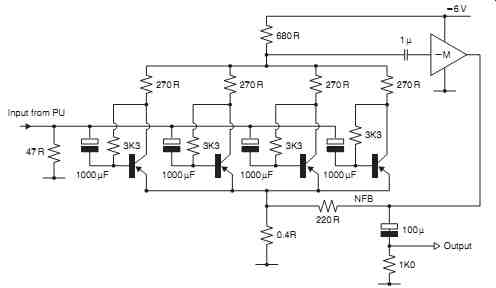
FIG. 5: Ortofon MCA-76 head amplifier.
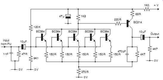
FIG. 6: The Naim NAC 20 moving coil head amplifier.
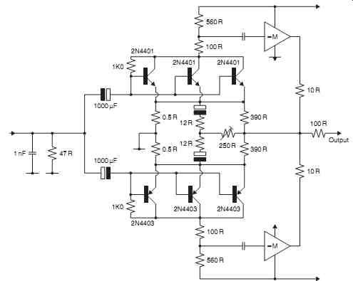
FIG. 7: Braithwaite RAI4 head amplifier. (The output stage is shown in a simplified form.)
This is achieved in the Ortofon circuit by individual collector-base bias current networks, for which the penalty is the loss of some usable signal in the collector circuit. In the Linn/Naim and Braithwaite designs, this evening out of transistor characteristics in circuits having common base connections is achieved by the use of individual emitter resistors to swamp such differences in device characteristics. In this case, the penalty is that such resistors add to the base-emitter circuit impedance when the task of the design is to reduce this.
6.3 Monolithic Super-Matched Input Devices
An alternative method of reducing the input circuit impedance, without the need for separate bias systems or emitter circuit-swamping resistors, is to employ a monolithic (integrated circuit type) device in which a multiplicity of transistors has been simultaneously formed on the same silicon chip. Since these can be assumed to have virtually identical characteristics, they can be paralleled, at the time of manufacture, to give a very low impedance, low noise, matched pair.
An example of this approach is the National Semiconductors LM 194/394 super-match pair, for which a suitable circuit is shown in FIG. 8. This input device probably offers the best input noise performance currently available, but is relatively expensive.
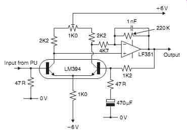
FIG. 8: Head amplifier using a LM394 multiple transistor array.
6.4 Small Power Transistors as Input Devices
The base-emitter impedance of a transistor depends largely on the size of the junction area on the silicon chip. This will be larger in power transistors than in small signal transistors, which mainly employ relatively small chip sizes. Unfortunately, the current gain of power transistors tends to decrease at low collector current levels, making them unsuitable for this application.
However, use of the plastic encapsulated medium power (3-4A l_c max.) styles, in T0126, T0127, and T0220 packages, at collector currents in the range of 1-3 mA, achieves a satisfactory compromise between input circuit impedance and transistor performance and allows the design of very linear low-noise circuitry. Two examples of MC head amplifier designs of this type, by the author, are shown in FIGs. 9 and 10 .
The penalty in this case is that, because such transistor types are not specified for low noise operation, some preliminary selection of the devices is desirable, although, in the writer's experience, the bulk of the devices of the types shown will be found to be satisfactory in this respect.
In the circuit shown in FIG. 9 , the input device is used in the common base (cascode) configuration so that the input current generated by the PU cartridge is transferred directly to the higher impedance point at the collector of this transistor so that the stage gain, prior to the application of negative feedback to the input transistor base, is simply the impedance transformation due to the input device.
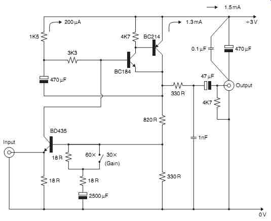
FIG. 9: Cascode input moving coil head amplifier.
The penalty in this case is that, because such transistor types are not specified for low noise operation, some preliminary selection of the devices is desirable, although, in the writer's experience, the bulk of the devices of the types shown will be found to be satisfactory in this respect.
In the circuit shown in FIG. 9 , the input device is used in the common base (cascode) configuration so that the input current generated by the PU cartridge is transferred directly to the higher impedance point at the collector of this transistor so that the stage gain, prior to the application of negative feedback to the input transistor base, is simply the impedance transformation due to the input device.
In the circuit of FIG. 10 , the input transistors are used in a more conventional common-emitter mode, but the two input devices, although in a push-pull configuration, are effectively connected in parallel so far as the input impedance and noise figure are concerned. The very high degree of symmetry of this circuit assists in minimizing both harmonic and transient distortions.
Both of these circuits are designed to operate from 3-V DC "pen cell" battery supplies to avoid the introduction of mains hum due to the power supply circuitry or to earth loop effects. In mains-powered head amps, great care is always necessary to avoid supply line signal or noise intrusions in view of the very low signal levels at both the inputs and the outputs of the amplifier stage.
It is also particularly advisable to design such amplifiers with single point "0-V " line and supply line connections, which should be coupled by a suitable combination of good quality decoupling capacitors.
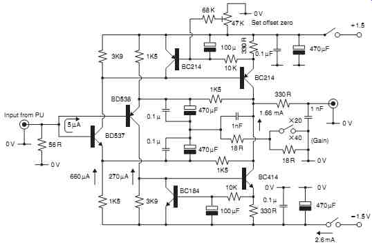
FIG. 10: Very low-noise, low-distortion, symmetrical MC head amplifier.
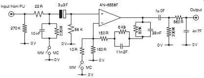
FIG. 11: Moving coil/moving magnet RIAA input stage in a Technics SU-V10 amplifier.
6.5 Very Low Noise IC Op-Amps
The development, some years ago, of very low noise IC operational amplifiers, such as the Precision Monolithics OP-27 and OP-37 devices, has led to the proliferation of very high-quality, low-noise, low-distortion ICs aimed specifically at the audio market, such as the Signetics NE-5532/ 5534, the NS LM833, the PMI SSM2134/2139, and the TI TL051/052 devices.
With ICs of this type, it is a simple matter to design a conventional RIAA input stage in which the provision of a high-sensitivity, low-noise, moving coil PU input is accomplished by simply reducing the value of the input load resistor and increasing the gain of the RIAA stage in comparison with that needed for higher output PU types. An example of a typical Japanese design of this type is shown in FIG. 11 .
6.6 Other Approaches
A very ingenious, fully symmetrical circuit arrangement that allows the use of normal circuit layouts and components in ultralow noise (e.g., moving coil PU and similar signal level) inputs has been introduced by "Quad" (Quad Electroacoustics Ltd.) and is employed in all their current series of preamps. This exploits the fact that, at low input signal levels, bipolar junction transistors will operate quite satisfactorily with their base and collector junctions at the same DC potential and permits the type of input circuit shown in FIG. 12 .
In the particular circuit shown, that used in the " Quad 44 " disc input, a two-stage equalization layout is employed, using the type of structure illustrated in FIG. 4(g) , with the gain of the second stage amplifier (a TL071 IC op-amp) switchable to suit the type of input signal level available.
== == ==