7. Input Connections
For all low-level input signals, care must be taken to ensure that the connections are of low contact resistance. This is obviously an important matter in the case of low impedance circuits such as those associated with MC PU inputs, but is also important in higher impedance circuitry, as the resistance characteristics of poor contacts are likely to be nonlinear, and to introduce both noise and distortion.
In the better class modern units, the input connectors will invariably be of the "phono" type, and both the plugs and the connecting sockets will be gold plated to reduce the problem of poor connections as a consequence of contamination or tarnishing of the metallic contacts.
The use of separate connectors for L and R channels also lessens the problem of interchannel breakthrough due to capacitative coupling or leakage across the socket surface, a problem that can arise in the ? ve- and seven-pin DIN connectors if they are fitted carelessly, particularly when both inputs and outputs are taken to that same DIN connector.
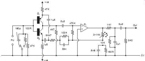
FIG. 12: The "Quad" ultralow noise input circuit layout.
8 Input Switching
The comments made about input connections are equally true for the necessary switching of the input signal sources. Separate, but mechanically interlinked, switches of the push on, push-off type are to be preferred to the ubiquitous rotary wafer switch, in that it is much easier, with separate switching elements, to obtain the required degree of isolation between inputs and channels than would be the case when the wiring is crowded around the switch wafer.
However, even with separate push switches, the problem remains that the input connections will invariably be made to the rear of the amplifier/preamplifier unit, whereas the switching function will be operated from the front panel so that the internal connecting leads must traverse the whole width of the unit.
Other switching systems, based on relays, or bipolar or field effect transistors, have been introduced to lessen the unwanted signal intrusions, which may arise on a lengthy connecting lead. The operation of a relay, which will behave simply as a remote switch when its coil is energized by a suitable DC supply, is straightforward, although for optimum performance it should either be hermetically sealed or have noble metal contacts to resist corrosion.
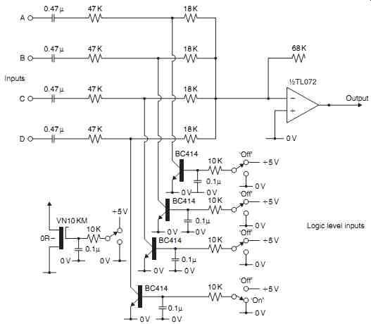
FIG. 13: Bipolar transistor-operated shunt switching. [Also suitable for small-power
metal-oxide-semiconductor field-effect transistor (MOSFET) devices.]
8.1 Transistor Switching
Typical bipolar and FET input switching arrangements are shown in FIGs. 13 and 14 . In the case of the bipolar transistor switch circuit of FIG. 13 , the nonlinearity of the junction device when conducting precludes its use in the signal line; the circuit is therefore arranged so that the transistor is nonconducting when the signal is passing through the controlled signal channel, but acts as a short-circuit to shunt the signal path to the 0-V line when it is caused to conduct.
In the case of the FET switch, if R1 and R2 are high enough, the nonlinearity of the conducting resistance of the FET channel will be swamped, and the harmonic and other distortions introduced by this device will be negligible (typically less than 0.02% at 1 V rms and 1 kHz).
The CMOS bilateral switches of the CD4066 type are somewhat nonlinear and have a relatively high level of breakthrough. For these reasons they are generally thought to be unsuitable for high-quality audio equipment where such remote switching is employed to minimize cross talk and hum pick up.
However, such switching devices could well offer advantages in lower quality equipment where the cost savings is being able to locate the switching element on the printed circuit board, at the point where it was required, might offset the device cost.
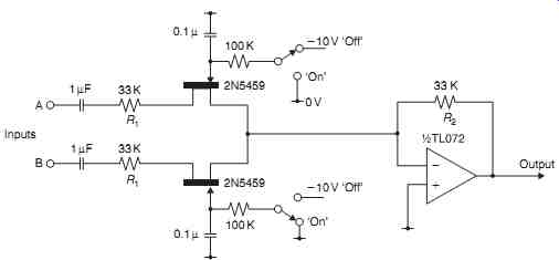
FIG. 14: Junction FET input switching circuit.
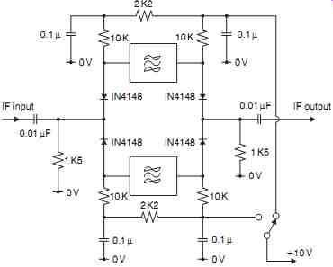
FIG. 15: Typical diode switching circuit, as used in RF applications.
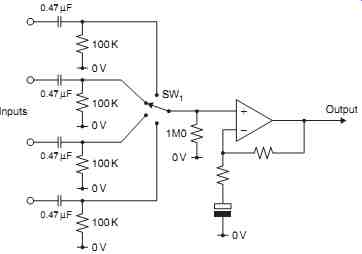
FIG. 16: Use of DC blocking capacitors to minimize input switching noises.
8.2 Diode Switching
Diode switching of the form shown in FIG. 15 , while employed very commonly in RF circuitry, is unsuitable for audio use because of the large shifts in the DC level between the " on " and " off " conditions, which would produce intolerable " bangs " on operation.
For all switching, quietness of operation is an essential requirement, and this demands that care shall be taken to ensure that all of the switched inputs are at the same DC potential, preferably that of the 0-V line. For this reason, it is customary to introduce DC blocking capacitors on all input lines, as shown in FIG. 16 , and the time constants of the input RC networks should be chosen so that there is no unwanted loss of low frequency signals due to this cause.
VOLTAGE AMPLIFIERS AND CONTROLS
9 Preamplifier Stages
The popular concept of hi-fi attributes the major role in final sound quality to the audio power amplifier and the output devices or output configuration that it uses. Yet in reality the preamplifier system, used with the power amplifier, has at least as large an influence on the final sound quality as the power amplifier, and the design of the voltage gain stages within the pre- and power amplifiers is just as important as that of the power output stages. Moreover, developments in the design of such voltage amplifier stages have allowed continuing improvement in amplifier performance.
The developments in solid-state linear circuit technology that have occurred over the past 30 years seem to have been inspired in about equal measure by the needs of linear integrated circuits and by the demands of high-quality audio systems; engineers working in both of these fields have watched each other's progress and borrowed from each other's designs.
In general, the requirements for voltage gain stages in both audio amplifiers and integrated-circuit operational amplifiers are very similar. These are that they should be linear, which implies that they are free from waveform distortion over the required output signal range, have as high a stage gain as is practicable, have a wide AC bandwidth and a low noise level, and are capable of an adequate output voltage swing.
The performance improvements that have been made over this period have been due in part to the availability of new or improved types of semiconductor devices and in part to a growing understanding of the techniques for the circuit optimization of device performance. The interrelation of these aspects of circuit design is considered next.
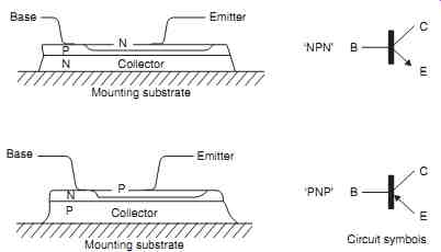
FIG. 17: Typical chip cross section of NPN and PNP silicon planar epitaxial
transistors.
== == ==