by Dr. Norman C. Thagard
Norman E. Thagard, M.D., a NASA astronaut, has been selected as the prime crew member for a three month flight on the Russian space station Mir in 1995. Dr. Thagard served as payload commander for STS-42 aboard the space shuttle Discovery during its 122-orbit flight in January 1992. With the completion of that mission, his fourth, he had logged over 604 hours in space. He has been awarded 11 air medals, including the Navy Commendation with Combat "V" and the Marine Corps "E" award, both while a tighter pilot in the Marine Corps. In addition to his M.D. degree, Dr. Thagard holds bachelor and master of science degrees in engineering science from FloridaStateUniversity. In his spare time, he enjoys electronic design and has published several articles, including an amp design done with NelsonPass in Audio Amateur's 4/92 issue.
-Gene Pitts
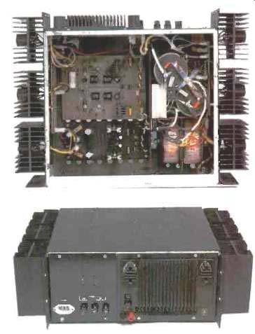
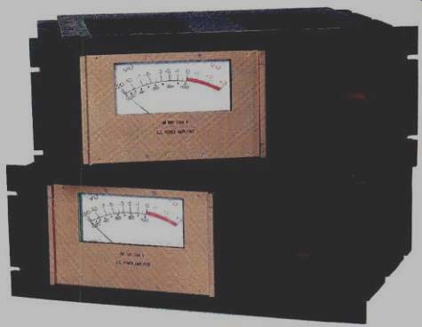
If can affordable amplifier possessing characteristics usually associated with the so-called 'high end" interests you, please read on. This construction article describes a mono power amplifier whose performance I believe to be exceptional. Al though the term "high end" has no precise definition, equipment so classified is generally expensive and represents, in the designer's view, an uncompromised fort to create a device superior in performance. The latter was certainly my intent, but the price was only a tow hundred dollars per channel. It takes a long string of words to thoroughly characterize the amplifier. How about "bi-FET input, bi-MOS output, cascoded, d.c. amplifier capable of 100 watts pure Class-A operation into 8 ohms at 0.1% or Less THD without global feedback"? I might add, "with slew rate greater than 100 V/uS."
Let me hasten to mention that I did not pick the topology and then proceed with a design. This project began with a list of design goals, and the topology was chosen as the only straightforward way to meet all of those goals. The goals were: (1) 100-watt pure Class-A operation into an 8-ohm load; (2) THD less than or equal to 0.1% at rated output; (3) low susceptibility to TIM; (4) immunity from load-induced instabilities, and (5) response down to d.c. These goals dictated most of the subsequent de sign decisions. Invariably, some choices were mandated by such mundane considerations as availability of parts. You might be surprised to learn that not every design choice is critical and absolute, so the de signer can be somewhat arbitrary at times.
It suffices to say that the resultant design met all five design goals. Since I hope this article can serve as a tutorial for those interested in modern power amplifier design, the whys and wherefores of this particular unit will be explained in some detail.
The requirement for 100-watt pure Class-A operation demands a hefty paralleled output stage with consequent high current demands from the driver stage if the more conventional, bipolar output transistors are used. Unfortunately, a Class A driver is, in many respects, the most difficult part of the design. An obvious way to gain stability into reactive loads is to avoid global feedback. But this results in increased distortion, which makes goal 2 harder to attain. I found that an output using medium-power MOS-FETs in common source, together with rugged bipolar power transistors in common base, in a "bi-MOS cascode" was an excellent way to simultaneously meet the first four design goals. Because the driver for such an output sees only the high impedance of MOS-FET gates, it is then fairly easy to develop a Class-A driver capable of slewing an output stage that idles at 2.5 amperes.
The fifth goal, d.c. operation, gave me fits. Those familiar with the thermal drift problems in d.c. amplifiers will appreciate this aspect of the design. I own a Crown DC300 and marvel at its d.c. performance. It uses a bipolar differential input stage operated at a fraction of 1 mA and consequently requires several current-gain stages. Similarly, to achieve acceptably low d.c. drift, I had to operate bipolar input devices at such low bias currents that an extra gain stage was required. Since I am convinced that fewer is often better, I finally abandoned bipolars in favor of J-FETs at the input. No special thermal compensation is employed; nonetheless, drift and offset are quite acceptable for an amplifier intended to reproduce sound.
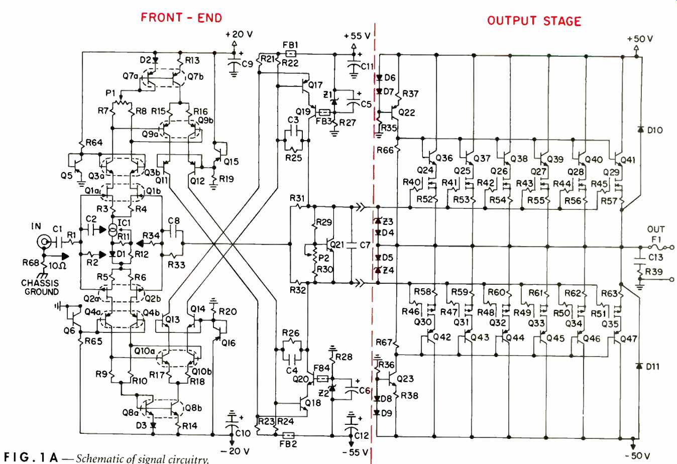
FIG. 1A--Schematic of signal circuitry.
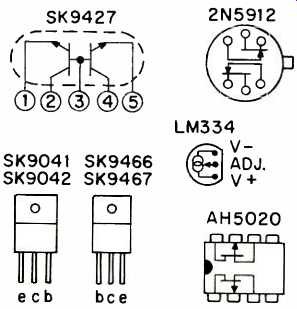
FIG.1B--Pinouts (top view) of the less common devices used; pinout for
SK9428 is identical to that for SK9427.
Building an amplifier with low TIM moves one in the direction of broad open-loop bandwidth and low to moderate levels of global feedback [1]. Lowering global feedback increases THD, which is undesirable. Cascoding both increases bandwidth by lowering the Miller capacitance and lowers distortion by incorporating common-base operation [2]. Therefore, all stages are cascoded.
I owe a large debt of gratitude to Nelson Pass, a highly regarded designer of high-end audio equipment (and my co-author on another design article). He provided both specific critiques and recommendations for improvement of this design and some sage philosophical advice. One such piece of advice concerned parts count and the use of five devices when one would do.
(A cascode has a significantly higher parts count than its non-cascoded brethren, but I did not think that I could reasonably meet design goals otherwise. The objective results of wide bandwidth and low distortion found here are undeniable.)
Circuit Description
Let us begin at the beginning, which is to say, at the input of the amplifier. (See schematic, Fig. 1.) The optional input capacitor, C1, is used to block d.c. The amp is essentially a gain of -20 voltage amplifier right down to d.c. If your preamp has any d.c. offset at its output, then 20 times the offset voltage will be presented to your speaker. Unless you are sure that your pre-amp has negligible offset, use capacitor C1; otherwise, simply use a wire shunt across the p.c. board where C1 would normally be placed. On the pattern provided, capacitors of various sizes can be accommodated. Use a good-quality film cap here; the prototype used a polypropylene part. With a value of 3 µF, low-frequency cutoff was less than 2 Hz when driven by a 600-ohm source.
The signal source's output impedance combines with resistors R1 and R2 and capacitor C2 to form a low-pass input filter with a cutoff of a couple hundred kilo hertz. Historically, I believe such input filters were for r.f.i. protection. This amp has outstanding high-frequency response, so such a filter is well advised.
Resistor R2 sets the input impedance to approximately 50 kilohms. I typically choose this value because it is high enough to preclude loading preamps with even a high output impedance while low enough to minimize stray coupling into excessively high input impedances. I have seen this latter problem occur in digital applications with FET inputs.
The input stage itself is a dual-differential "bi-FET" cascode using roughly complementary p- and n-channel J-FETs in common source with complementary PNP and NPN bipolars in common base. All transistors in this stage are matched dual devices in order to minimize offset and drift. The 2N5912s used for transistor Q1 may be difficult to obtain these days. Two units were constructed using closely matched 2N4391s. These n-channel single J-FETs are widely available and are inexpensive. RCA (in its SK series) as well as other manufacturers of replacement devices offer dual n-channel J FETs. However, J-FETs with an Ids, greater than 2 mA are required, so check the specs before using a particular transistor. The units using a pair of single J-FETs worked fine.
The first stage's d.c. bias is set to 1 mA by adjusting the monolithic constant-current source, ICI, to 2 mA. Integrated circuit IC1 offers programmable current sourcing by selection of R11 and R12.
The selected values for R11, R12, and D1 also reduce current variations, which improves d.c. performance. Notice that IC1 is a common current source for both halves of the dual-differential stage. This is made possible because J-FETs Q1 and Q2 are depletion-mode devices, which results in a voltage differential between p- and n-channel sources large enough to permit proper operation of IC1.
The cascode bias is set by the zener-connected transistors Q5 and Q6. I borrowed this idea from Nelson Pass. The NPN MPSA42s and their PNP complement MPSA92s, manufactured by Motorola, used to give a very constant 7-V when so operated. However, the newer MPSA42s no longer give such a voltage, and you may find the specified MPSA92s do not give 7-V either. You can substitute 7-V zeners for Q5, Q6, Q15, and Q16; decrease R19, R20, R64, and R65 to 2.2 kilohms if you make this substitution. Also, bypass the zeners with 10-µF, 16-V electrolytic capacitors to minimize zener noise.
The 7-V figure is not critical, but too low a value will impair the input dynamic range and may defeat the cascode. Earlier versions of this design "floated" the cascode bias. While that gave very wide dynamic range and was theoretically superior, it was appreciably more complex.
Objective measurements failed to demonstrate an advantage, so the scheme was abandoned. Proper cascode biasing places the J-FETs in their constant-current region.
For a solved cascode design example, see [3, in Part II of this article].
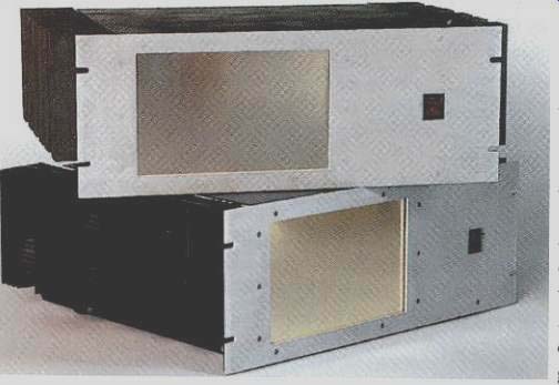
above: An alternate version of the amp, without meters and using commercial
heat-sinks, built by a friend of the author.
Trimpot P1 provides for output offset nulling. Its adjustment range is intention- ally small so that the chance of inadvertently causing large offsets is lessened. If the offset could not be nulled with P1, it would be a clue that something is wrong.
The first stage's output is directly coupled to the second stage, which is also a dual-differential arrangement. Cascading (not cascoding) differential stages has advantages for thermal stability, since drifts in earlier stages tend to cancel out [4]. The disadvantage is an increased parts count, but this d.c. stability is important enough to justify the complexity in a largely no-compromise effort.
The second stage is d.c. biased by a nice scheme: The 2 mA generated in the first stage by IC1 is run through diodes D2 and D3 to create a 0.7-V reference for the constant-current-configured transistors Q7b and Q8b.
Resistors R13 and R14 are 43 ohms, so the current sources generate 16 mA (0.7 divided by 43), or 8 mA through each leg of the differential pair. Since Q7 and Q8 are dual devices, they should perform well as constant current sources.
The common-emitter transistors, Q9 and Q10, of the second-stage cascode are again matched duals to lower drift. However, that consideration is not as important in this stage, and the common-base devices, Q11 through Q14, are not duals. (Indeed, I could find no dual devices with the voltage and power ratings required in this application.) Transistors Q11 through Q14 perform a d.c. level shift from the 20-V input rails to the 55-V driver rails and therefore have almost 70 V across them.
I realize that some may wonder about the use of separate power rails for input and driver stages. There are, however, ad vantages which justify this. Operating the input at 55 V would increase the thermal dissipation of that stage, which would de grade d.c. performance. Audio performance can be impaired by signal coupling through the power supply; the separate supply helps with this potential problem.
Finally, the 20-V rail is derived from the al ready regulated 55-V rail via a second voltage regulator, thereby providing the most critical stage with doubly regulated power supplies.
The second stage is again directly coupled to the following one-in this case, the driver. Since the driver supplies most of the voltage gain found in the amp and a fair amount of current gain as well, it is, in many respects, the toughest stage to realize.
This stage is, in effect, the output stage of a low-power amplifier in its own right. Be cause the output uses MOS-FETs in common-source configuration, the driver is spared the necessity of providing several hundred milliamperes, as would be the case if the output comprised bipolar transistors. As has been acknowledged, the gate of a MOS-FET represents essentially a capacitive load. Therefore, drive current needs only to be high enough to charge and discharge that gate capacitance rapidly enough to achieve acceptable output slew rates. Suffice it to say that biasing the driver at about 60 mA gives enough capability to handle the 2-nF load that the output MOS FETs present to it. The 100-V/uS slew rate is testimony to this! The drive stage's bias is determined by the voltage across R22 and R24, which is, in turn, set by the 8-mA bias current from the second stage. Thus, Vb., is 2.66 V (0.008 times 332), and R21 and R23 see this 2.66 V less the base-to-emitter voltage of Q17 and Q18 (0.7 V), for a net of 1.96 V. Resistors R21 and R23 are 30.1 ohms; 1.96 di vided by this figure yields 65 mA. However, 8 mA of this 65 mA is furnished by the second stage bias, so that driver-stage bias is 57 mA (65 minus 8). Excellent power band width is achieved with this bias level.
Zener diodes Z1 and Z2 provide cascode bias for the driver stage. Capacitors C5 and C6 help reduce the noise inherent in zener operation.
The ferrite beads, FBI through FB4, are essentially small, lossy inductors. Their use nicely tamed some high-frequency oscillations which were present. Such oscillations are not unusual in extended band width designs but would be unacceptable if unsuppressed. A major advantage of the beads is that they can obviate the need for bandwidth-robbing capacitors; a potential disadvantage is that their saturation can produce distortion. Current levels through these beads are too small to cause a problem here.
The voltage gain of the driver cascode was 1,600. This was so high that compensating the closed-loop front-end and still having any band width remaining was a problem. In keeping with the theme of only low to moderate levels of open-loop gain, R25 and R26 were added to provide local feedback. With their addition, the driver stage's gain then becomes roughly 100 (the value of R25 di vided by the value of R22 or, similarly, R26 divided by R24). With the reduction in gain realized with local feedback, the small capacitors C3 and C4 were all that were required to compensate the closed-loop front-end. With the 47-pF caps used, open-loop bandwidth was well in excess of 20 kHz, the design goal set to preclude TIM. Open-loop voltage gain was about 56 dB, a good level.
Further installments of this article will cover the power supply, the output stage, construction methods, and the amp's operation. A complete Parts List and references will be provided.
===================
On the Test Bench

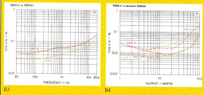
Measurements of the amplifier, taken by Nelson Pass at Pass Laboratories,
of frequency response (Figs. B1 and B2), THD + N vs. frequency (Fig. B3),
and THD + N vs. output (Fig. B4).
===================
(adapted from Audio magazine, Jan. 1995)
= = = =